background image

www.ti.com

Functional Description

603

SLAU723A – October 2017 – Revised October 2018

Submit Documentation Feedback

Copyright © 2017–2018, Texas Instruments Incorporated

Micro Direct Memory Access (µDMA)

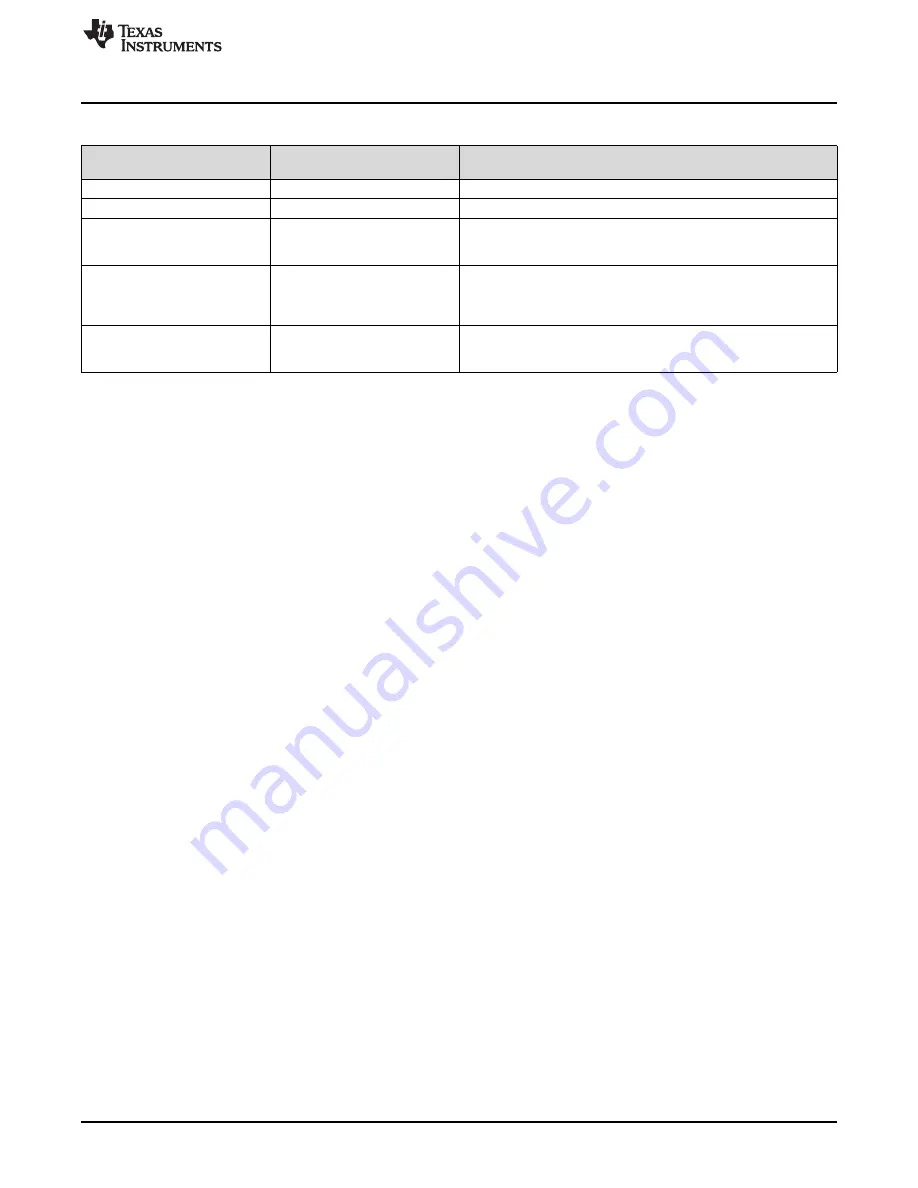
Table 8-1. Request Type Support (continued)

Peripheral

Event That Generates Single

Request

Event That Generates Burst Request

UART TX

TX FIFO not full

TX FIFO level (configurable)

UART RX

RX FIFO not empty

RX FIFO level (configurable)

SHA/MD5

None

Context in DMA request (SHA/MD5 0 Cin)
Context out DMA request (SHA/MD5 0 Cout)
Data In DMA request (SHA/MD5 0 Din)

AES

None

Context in DMA request (AES0 Cin)
Context out DMA request (AES0 Cout)
Data in DMA request (AES0 Din)
Data out DMA request (AES0 Dout)

DES

None

Context in DMA request (DES0 Cin)
Data in DMA request (DES0 Din)
Data out DMA request (DES0 Dout)

8.3.3.1

Single Request

When a single request is detected, and not a burst request, the µDMA controller transfers one item and
then stops to wait for another request.

8.3.3.2

Burst Request

When a burst request is detected, the µDMA controller transfers the number of items that is the lesser of
the arbitration size or the number of items remaining in the transfer. Therefore, the arbitration size should
be the same as the number of data items that the peripheral can accommodate when making a burst
request. For example, the UART generates a burst request based on the FIFO trigger level. In this case,
the arbitration size should be set to the amount of data that the FIFO can transfer when the trigger level is
reached. A burst transfer runs to completion once it is started, and cannot be interrupted, even by a higher
priority channel. Burst transfers complete in a shorter time than the same number of non-burst transfers.

It may be desirable to use only burst transfers and not allow single transfers. For example, perhaps the
nature of the data is such that it only makes sense when transferred together as a single unit rather than
one piece at a time. The single request can be disabled by using the DMA Channel Useburst Set
(DMAUSEBURSTSET) register. By setting the bit for a channel in this register, the µDMA controller only
responds to burst requests for that channel.

8.3.4 Channel Configuration

The µDMA controller uses an area of system memory to store a set of channel control structures in a
table. The control table may have one or two entries for each µDMA channel. Each entry in the table
structure contains source and destination pointers, transfer size, and transfer mode. The control table can
be located anywhere in system memory, but it must be contiguous and aligned on a 1024-byte boundary.

Table 8-2

lists the layout in memory of the channel control table. Each channel may have one or two

control structures in the control table: a primary control structure and an optional alternate control
structure. The table is organized so that all of the primary entries are in the first half of the table, and all
the alternate structures are in the second half of the table. The primary entry is used for simple transfer
modes where transfers can be reconfigured and restarted after each transfer is complete. In this case, the
alternate control structures are not used and therefore only the first half of the table must be allocated in
memory; the second half of the control table is not necessary, and that memory can be used for
something else. If a more complex transfer mode is used such as ping-pong or scatter-gather, then the
alternate control structure is also used and memory space should be allocated for the entire table.

Any unused memory in the control table may be used by the application. This includes the control
structures for any channels that are unused by the application as well as the unused control word for each
channel.

Содержание SimpleLink Ethernet MSP432E401Y

Страница 1: ...MSP432E4 SimpleLink Microcontrollers Technical Reference Manual Literature Number SLAU723A October 2017 Revised October 2018...

Страница 2: ...Behavior of Memory Accesses 100 1 5 4 Software Ordering of Memory Accesses 101 1 5 5 Bit Banding 102 1 5 6 Data Storage 104 1 5 7 Synchronization Primitives 104 1 6 Exception Model 105 1 6 1 Exception...

Страница 3: ...t 0xD14 reset 0x200 156 2 5 8 SYSPRI1 Register Offset 0xD18 reset 0x0 157 2 5 9 SYSPRI2 Register Offset 0xD1C reset 0x0 158 2 5 10 SYSPRI3 Register Offset 0xD20 reset 0x0 159 2 5 11 SYSHNDCTRL Registe...

Страница 4: ...250 4 2 18 PIOSCSTAT Register Offset 0x154 reset 0x00400040 251 4 2 19 PLLFREQ0 Register Offset 0x160 reset 0x0 252 4 2 20 PLLFREQ1 Register Offset 0x164 reset 0x0 253 4 2 21 PLLSTAT Register Offset...

Страница 5: ...EPI Register Offset 0x510 reset 0x00 305 4 2 69 SRHIB Register Offset 0x514 reset 0x00 306 4 2 70 SRUART Register Offset 0x518 reset 0x00 307 4 2 71 SRSSI Register Offset 0x51C reset 0x0 309 4 2 72 SR...

Страница 6: ...EI Register Offset 0x744 reset 0x0 365 4 2 122 SCGCEEPROM Register Offset 0x758 reset 0x0 366 4 2 123 SCGCCCM Register Offset 0x774 reset 0x0 367 4 2 124 SCGCLCD Register Offset 0x790 reset 0x0 368 4...

Страница 7: ...0x0 445 4 2 173 PREPI Register Offset 0xA10 reset 0x0 446 4 2 174 PRHIB Register Offset 0xA14 reset 0x1 447 4 2 175 PRUART Register Offset 0xA18 reset 0x00 448 4 2 176 PRSSI Register Offset 0xA1C res...

Страница 8: ...x0 502 6 5 6 HIBRIS Register Offset 0x18 reset 0x0 504 6 5 7 HIBMIS Register Offset 0x1C reset 0x0 506 6 5 8 HIBIC Register Offset 0x20 reset 0x0 508 6 5 9 HIBRTCT Register Offset 0x24 reset 0x7FFF 51...

Страница 9: ...Register Offset 0x4 reset 0x0 573 7 4 3 EEOFFSET Register Offset 0x8 reset 0x0 574 7 4 4 EERDWR Register Offset 0x10 reset X 575 7 4 5 EERDWRINC Register Offset 0x14 reset X 576 7 4 6 EEDONE Register...

Страница 10: ...Register Offset 0x20 reset 0x0 636 8 6 10 DMAREQMASKCLR Register Offset 0x24 reset X 637 8 6 11 DMAENASET Register Offset 0x28 reset 0x0 638 8 6 12 DMAENACLR Register Offset 0x2C reset X 639 8 6 13 DM...

Страница 11: ...0 698 9 6 2 AES_DMARIS Register Offset 0x24 reset 0x0 699 9 6 3 AES_DMAMIS Register Offset 0x28 reset 0x0 700 9 6 4 AES_DMAIC Register Offset 0x2C reset 0x0 701 10 Analog to Digital Converter ADC 702...

Страница 12: ...ffset 0xD00 reset 0x0 775 10 5 36 ADCDCCTL0 to ADCDCCTL7 Registers reset 0x0 779 10 5 37 ADCDCCMP0 to ADCDCCMP7 Registers reset 0x0 781 10 5 38 ADCPP Register Offset 0xFC0 reset 0x01B02187 782 10 5 39...

Страница 13: ...Register Offset 0x8 reset 0x0 837 12 5 4 ACREFCTL Register Offset 0x10 reset 0x0 838 12 5 5 ACSTATn Register reset 0x0 839 12 5 6 ACCTLn Register reset 0x0 840 12 5 7 ACMPPP Register Offset 0xFC0 rese...

Страница 14: ...2 Block Diagram 884 15 3 Functional Description 884 15 3 1 Ethernet Clock Control 884 15 3 2 MII and RMII Signals 887 15 3 3 DMA Controller 888 15 3 4 TX RX Controller 909 15 3 5 MAC Operation 913 15...

Страница 15: ...0x180 reset 0x0 990 15 6 35 EMACRXCNTCRCERR Register Offset 0x194 reset 0x0 991 15 6 36 EMACRXCNTALGNERR Register Offset 0x198 reset 0x0 992 15 6 37 EMACRXCNTGUNI Register Offset 0x1C4 reset 0x0 993...

Страница 16: ...9 reset 0x0 1059 15 7 11 EPHYCFG2 Register Address 0xA reset 0x4 1061 15 7 12 EPHYCFG3 Register Address 0xB reset 0x0 1062 15 7 13 EPHYREGCTL Register Address 0xD reset 0x0 1063 15 7 14 EPHYADDAR Regi...

Страница 17: ...4 1161 16 5 22 EPIMIS Register Offset 0x218 reset 0x0 1163 16 5 23 EPIEISC Register Offset 0x21C reset 0x0 1165 16 5 24 EPIHB8CFG3 Register Offset 0x308 reset 0x00080000 1166 16 5 25 EPIHB16CFG3 Regis...

Страница 18: ...gister Offset 0x540 reset 0x0 1235 17 5 28 GPIOWAKELVL Register Offset 0x544 reset 0x0 1236 17 5 29 GPIOWAKESTAT Register Offset 0x548 reset 0x0 1237 17 5 30 GPIOPP Register Offset 0xFC0 reset 0x1 123...

Страница 19: ...8 5 19 GPTMTBR Register Offset 0x4C reset 0xFFFF 1301 18 5 20 GPTMTAV Register Offset 0x50 reset 0xFFFFFFFF 1302 18 5 21 GPTMTBV Register Offset 0x54 reset 0xFFFF 1303 18 5 22 GPTMRTCPD Register Offse...

Страница 20: ...5 27 I2CPC Register Offset 0xFC4 reset 0x1 1376 20 LCD Controller 1377 20 1 Introduction 1378 20 2 Block Diagram 1378 20 3 Functional Description 1379 20 3 1 Clocking 1379 20 3 2 LCD DMA Engine 1380...

Страница 21: ...mparators 1439 21 3 4 PWM Signal Generator 1440 21 3 5 Dead Band Generator 1441 21 3 6 Interrupt or ADC Trigger Selector 1441 21 3 7 Synchronization Methods 1441 21 3 8 Fault Conditions 1442 21 3 9 Ou...

Страница 22: ...RECS Register Offset 0x0 reset 0x0 1511 22 5 2 ONEWIRETIM Register Offset 0x4 reset 0x0 1513 22 5 3 ONEWIREDATW Register Offset 0x8 reset 0x0 1514 22 5 4 ONEWIREDATR Register Offset 0xC reset 0x0 1515...

Страница 23: ...Encoder Interface QEI 1567 24 1 Introduction 1568 24 2 Block Diagram 1568 24 3 Functional Description 1570 24 4 Initialization and Configuration 1572 24 5 QEI Registers 1573 24 5 1 QEICTL Register Of...

Страница 24: ...UARTECR Register Offset 0x4 reset 0x0 1634 26 5 3 UARTFR Register Offset 0x18 reset 0x90 1635 26 5 4 UARTILPR Register Offset 0x20 reset 0x0 1637 26 5 5 UARTIBRD Register Offset 0x24 reset 0x0 1638 2...

Страница 25: ...1709 27 5 9 USBFRAME Register Offset 0xC reset 0x0 1711 27 5 10 USBEPIDX Register Offset 0xE reset 0x0 1712 27 5 11 USBTEST Register Offset 0xF reset 0x0 1713 27 5 12 USBFIFOn Register reset 0x0 1715...

Страница 26: ...2 27 5 59 USBHSBT Register Offset 0x348 reset 0x0 1773 27 5 60 USBLPMATTR Register Offset 0x360 reset 0x0 1774 27 5 61 USBLPMCNTRL Register Offset 0x362 reset 0x0 1775 27 5 62 USBLPMIM Register Offset...

Страница 27: ...0 reset 0x0 1810 28 5 10 WDTPeriphID5 Register Offset 0xFD4 reset 0x0 1810 28 5 11 WDTPeriphID6 Register Offset 0xFD8 reset 0x0 1811 28 5 12 WDTPeriphID7 Register Offset 0xFDC reset 0x0 1811 28 5 13 W...

Страница 28: ...111 2 1 SRD Use Example 127 2 2 FPU Register Bank 129 2 3 STCTRL Register 134 2 4 STRELOAD Register 135 2 5 STCURRENT Register 136 2 6 EN0 to EN3 Registers 139 2 7 DISn Register 140 2 8 PENDn Registe...

Страница 29: ...odule Clock Selection 213 4 7 DID0 Register 222 4 8 DID1 Register 224 4 9 PTBOCTL Register 226 4 10 RIS Register 227 4 11 IMC Register 229 4 12 MISC Register 230 4 13 RESC Register 232 4 14 PWRTC Regi...

Страница 30: ...56 PPI2C Register 286 4 57 PPUSB Register 287 4 58 PPEPHY Register 288 4 59 PPCAN Register 289 4 60 PPADC Register 290 4 61 PPACMP Register 291 4 62 PPPWM Register 292 4 63 PPQEI Register 293 4 64 PPE...

Страница 31: ...Register 341 4 107 RCGCEEPROM Register 342 4 108 RCGCCCM Register 343 4 109 RCGCLCD Register 344 4 110 RCGCOWIRE Register 345 4 111 RCGCEMAC Register 346 4 112 SCGCWD Register 347 4 113 SCGCTIMER Reg...

Страница 32: ...395 4 154 PCWD Register 396 4 155 PCTIMER Register 398 4 156 PCGPIO Register 401 4 157 PCDMA Register 405 4 158 PCEPI Register 407 4 159 PCHIB Register 409 4 160 PCUART Register 411 4 161 PCSSI Regist...

Страница 33: ...s the Hibernation Clock Source with VDD3ON Mode 480 6 4 Using a Regulator for Both VDD and VBAT 481 6 5 Counter Behavior with a TRIM Value of 0x8002 484 6 6 Counter Behavior with a TRIM Value of 0x7FF...

Страница 34: ...ster 561 7 16 FWBVAL Register 562 7 17 FLPEKEY Register 563 7 18 FWBn Register 564 7 19 FLASHPP Register 565 7 20 SSIZE Register 566 7 21 FLASHCONF Register 567 7 22 ROMSWMAP Register 568 7 23 FLASHDM...

Страница 35: ...ster 636 8 19 DMAREQMASKCLR Register 637 8 20 DMAENASET Register 638 8 21 DMAENACLR Register 639 8 22 DMAALTSET Register 640 8 23 DMAALTCLR Register 641 8 24 DMAPRIOSET Register 642 8 25 DMAPRIOCLR Re...

Страница 36: ...of Two ADC Blocks 703 10 2 ADC Module Block Diagram 704 10 3 ADC Sample Phases 708 10 4 Doubling the ADC Sample Rate 708 10 5 Skewed Sampling 709 10 6 Sample Averaging Example 710 10 7 ADC Input Equi...

Страница 37: ...r 775 10 50 ADCDCCTLn Register 779 10 51 ADCDCCMPn Register 781 10 52 ADCPP Register 782 10 53 ADCPC Register 784 10 54 ADCCC Register 785 11 1 CAN Controller Block Diagram 787 11 2 CAN Data Frame or...

Страница 38: ...4 12 DES_LENGTH Register 868 14 13 DES_DATA_L Register 869 14 14 DES_DATA_H Register 870 14 15 DES_REVISION Register 871 14 16 DES_SYSCONFIG Register 872 14 17 DES_SYSSTATUS Register 873 14 18 DES_IRQ...

Страница 39: ...33 EMACADDR1H Register 971 15 34 EMACADDR1L Register 972 15 35 EMACADDR2H Register 973 15 36 EMACADDR2L Register 974 15 37 EMACADDR3H Register 975 15 38 EMACADDR3L Register 976 15 39 EMACWDOGTO Regist...

Страница 40: ...ister 1034 15 81 EMACHOSTXBA Register 1035 15 82 EMACHOSRXBA Register 1036 15 83 EMACPP Register 1037 15 84 EMACPC Register 1038 15 85 EMACCC Register 1041 15 86 EPHYRIS Register 1042 15 87 EPHYIM Reg...

Страница 41: ...d Address and Data and ALE With Dual or Quad CSn 1114 16 16 Continuous Read Mode Accesses 1114 16 17 Write Followed by Read to External FIFO 1115 16 18 Two Entry FIFO 1115 16 19 Single Cycle Single Wr...

Страница 42: ...16 62 EPIHB16TIME3 Register 1184 16 63 EPIHB8TIME4 Register 1186 16 64 EPIHB16TIME4 Register 1188 16 65 EPIHBPSRAM Register 1190 17 1 Digital I O Pads 1193 17 2 Analog and Digital I O Pads 1194 17 3 G...

Страница 43: ...7 GPIOPCellID3 Register 1252 18 1 GPTM Module Block Diagram 1255 18 2 Input Edge Count Mode Example Counting Down 1261 18 3 16 Bit Input Edge Time Mode Example 1262 18 4 16 Bit PWM Mode Example 1263 1...

Страница 44: ...Transmit 1330 19 13 Master Transmit With Repeated START After Master Receive 1330 19 14 Standard High Speed Mode Master Transmit 1331 19 15 Slave Command Sequence 1332 19 16 I2CMSA Register 1336 19 1...

Страница 45: ...Register 1398 20 17 LCDCTL Register 1399 20 18 LCDLIDDCTL Register 1401 20 19 LIDDCS0CFG Register 1403 20 20 LIDDCS0ADDR Register 1404 20 21 LIDDCS0DATA Register 1405 20 22 LIDDCS1CFG Register 1406 2...

Страница 46: ...Register 1480 21 27 PWMnGENB Register 1482 21 28 PWMnDBCTL Register 1484 21 29 PWMnDBRISE Register 1485 21 30 PWMnDBFALL Register 1486 21 31 PWMnFLTSRC0 Register 1487 21 32 PWMnFLTSRC1 Register 1489 2...

Страница 47: ...545 23 15 SSIIM Register 1546 23 16 SSIRIS Register 1547 23 17 SSIMIS Register 1549 23 18 SSIICR Register 1551 23 19 SSIDMACTL Register 1552 23 20 SSIPP Register 1553 23 21 SSICC Register 1554 23 22 S...

Страница 48: ...26 4 UARTDR Register 1633 26 5 UARTRSR UARTECR Register 1634 26 6 UARTFR Register 1635 26 7 UARTILPR Register 1637 26 8 UARTIBRD Register 1638 26 9 UARTFBRD Register 1639 26 10 UARTLCRH Register 1640...

Страница 49: ...er 1719 27 22 ULPIVBUSCTL Register 1720 27 23 ULPIREGDATA Register 1721 27 24 ULPIREGADDR Register 1722 27 25 ULPIREGCTL Register 1723 27 26 USBEPINFO Register 1724 27 27 USBRAMINFO Register 1725 27 2...

Страница 50: ...USBCTO Register 1771 27 69 USBHHSRTN Register 1772 27 70 USBHSBT Register 1773 27 71 USBLPMATTR Register 1774 27 72 USBLPMCNTRL Register OTG A Host 1775 27 73 USBLPMCNTRL Register OTG B Device 1775 27...

Страница 51: ...er 1809 28 10 WDTPeriphID4 Register 1810 28 11 WDTPeriphID5 Register 1810 28 12 WDTPeriphID6 Register 1811 28 13 WDTPeriphID7 Register 1811 28 14 WDTPeriphID0 Register 1812 28 15 WDTPeriphID1 Register...

Страница 52: ...Exception Types 107 1 20 Exception Return Behavior 112 1 21 Faults 113 1 22 Fault Status and Fault Address Registers 114 1 23 Cortex M4F Instruction Summary 116 2 1 Core Peripheral Register Regions 12...

Страница 53: ...scriptions 171 2 45 MPUNUMBER Register Field Descriptions 172 2 46 MPUBASEn Register Field Descriptions 173 2 47 Example SIZE Field Values 175 2 48 MPUATTRn Register Field Descriptions 176 2 49 FPU Re...

Страница 54: ...59 4 38 LDOSPCTL Register Field Descriptions 259 4 39 LDOSPCAL Register Field Descriptions 260 4 40 LDODPCTL Register Field Descriptions 261 4 41 LDODPCAL Register Field Descriptions 262 4 42 SDPMST R...

Страница 55: ...88 SRCAN Register Field Descriptions 314 4 89 SRADC Register Field Descriptions 315 4 90 SRACMP Register Field Descriptions 316 4 91 SRPWM Register Field Descriptions 317 4 92 SRQEI Register Field Des...

Страница 56: ...egister Field Descriptions 367 4 137 SCGCLCD Register Field Descriptions 368 4 138 SCGCOWIRE Register Field Descriptions 369 4 139 SCGCEMAC Register Field Descriptions 370 4 140 DCGCWD Register Field...

Страница 57: ...186 PCADC Register Field Descriptions 425 4 187 Module Power Control 426 4 188 PCACMP Register Field Descriptions 427 4 189 Module Power Control 428 4 190 PCPWM Register Field Descriptions 429 4 191...

Страница 58: ...gurations 478 6 2 HIB Registers 493 6 3 HIB Access Type Codes 494 6 4 HIBRTCC Register Field Descriptions 495 6 5 HIBRTCM0 Register Field Descriptions 496 6 6 HIBRTCLD Register Field Descriptions 497...

Страница 59: ...riptions 567 7 21 ROMSWMAP Register Field Descriptions 568 7 22 FLASHDMASZ Register Field Descriptions 569 7 23 FLASHDMAST Register Field Descriptions 570 7 24 EEPROM Registers 571 7 25 EEPROM Access...

Страница 60: ...ions 629 8 22 DMACTLBASE Register Field Descriptions 630 8 23 DMAALTBASE Register Field Descriptions 631 8 24 DMAWAITSTAT Register Field Descriptions 632 8 25 DMASWREQ Register Field Descriptions 633...

Страница 61: ...rs 697 9 22 AES DMA Access Type Codes 697 9 23 AES_DMAIM Register Field Descriptions 698 9 24 AES_DMARIS Register Field Descriptions 699 9 25 AES_DMAMIS Register Field Descriptions 700 9 26 AES_DMAIC...

Страница 62: ...774 10 44 ADCSSTSH3 Register Field Descriptions 774 10 45 ADCDCRIC Register Field Descriptions 775 10 46 ADCDCCTLn Register Field Descriptions 779 10 47 ADCDCCMPn Register Field Descriptions 781 10 4...

Страница 63: ...46 13 4 CRC Access Type Codes 846 13 5 CRCCTRL Register Field Descriptions 847 13 6 CRCSEED Register Field Descriptions 849 13 7 CRCDIN Register Field Descriptions 850 13 8 CRCRSLTPP Register Field De...

Страница 64: ...nd Bit 24 of TDES0 925 15 20 Forced Mode Configurations 931 15 21 Advertised Mode Configurations 931 15 22 EMACPC to PHY Register Mapping 936 15 23 EMAC Registers 939 15 24 EMAC Access Type Codes 941...

Страница 65: ...ons 1001 15 68 EMACTIMSECU Register Field Descriptions 1002 15 69 EMACTIMNANOU Register Field Descriptions 1003 15 70 EMACTIMADD Register Field Descriptions 1004 15 71 EMACTARGSEC Register Field Descr...

Страница 66: ...escriptions 1067 15 117 EPHYMISR1 Register Field Descriptions 1069 15 118 EPHYMISR2 Register Field Descriptions 1071 15 119 EPHYFCSCR Register Field Descriptions 1073 15 120 EPHYRXERCNT Register Field...

Страница 67: ...C Register Field Descriptions 1165 16 37 EPIHB8CFG3 Register Field Descriptions 1166 16 38 EPIHB16CFG3 Register Field Descriptions 1168 16 39 EPIHB8CFG4 Register Field Descriptions 1170 16 40 EPIHB16C...

Страница 68: ...Register Field Descriptions 1235 17 39 GPIOWAKELVL Register Field Descriptions 1236 17 40 GPIOWAKESTAT Register Field Descriptions 1237 17 41 GPIOPP Register Field Descriptions 1238 17 42 GPIO Drive...

Страница 69: ...r Field Descriptions 1302 18 32 GPTMTBV Register Field Descriptions 1303 18 33 GPTMRTCPD Register Field Descriptions 1304 18 34 GPTMTAPS Register Field Descriptions 1305 18 35 GPTMTBPS Register Field...

Страница 70: ...LCD Access Type Codes 1397 20 8 LCDPID Register Field Descriptions 1398 20 9 LCDCTL Register Field Descriptions 1399 20 10 SYSCLK to Pixel Clock LCDCP Frequency Conversion Table 1400 20 11 LCDLIDDCTL...

Страница 71: ...iptions 1478 21 21 PWMnCMPB Register Field Descriptions 1479 21 22 PWMnGENA Register Field Descriptions 1480 21 23 PWMnGENB Register Field Descriptions 1482 21 24 PWMnDBCTL Register Field Descriptions...

Страница 72: ...criptions 1557 23 21 SSIPeriphID7 Register Field Descriptions 1558 23 22 SSIPeriphID0 Register Field Descriptions 1559 23 23 SSIPeriphID1 Register Field Descriptions 1560 23 24 SSIPeriphID2 Register F...

Страница 73: ...A_DMARIS Register Field Descriptions 1617 25 29 SHA_DMAMIS Register Field Descriptions 1618 25 30 SHA_DMAIC Register Field Descriptions 1619 26 1 Flow Control Mode 1626 26 2 UART Registers 1631 26 3 U...

Страница 74: ...eld Descriptions OTG A Host 1707 27 15 USBIS Register Field Descriptions OTG B Device 1708 27 16 USBIE Register Field Descriptions OTG A Host 1709 27 17 USBIE Register Field Descriptions OTG B Device...

Страница 75: ...758 27 62 USBTXTYPEn Register Field Descriptions 1759 27 63 USBTXINTERVALn Register Values 1760 27 64 USBTXINTERVALn Register Field Descriptions 1760 27 65 USBRXTYPEn Register Field Descriptions 1761...

Страница 76: ...scriptions 1802 28 5 WDTCTL Register Field Descriptions 1803 28 6 WDTICR Register Field Descriptions 1805 28 7 WDTRIS Register Field Descriptions 1806 28 8 WDTMIS Register Field Descriptions 1807 28 9...

Страница 77: ...ortex M4 Devices Generic User Guide IEEE Standard 1149 1 Test Access Port and Boundary Scan Architecture Documentation Conventions The following table lists the conventions used in this document Notat...

Страница 78: ...al names are in uppercase An overbar on a signal name indicates that it is active low To assert SIGNAL is to drive it low to deassert SIGNAL is to drive it high SIGNAL Signal names are in uppercase An...

Страница 79: ...igh performance low cost platform that meets the system requirements of minimal memory implementation reduced pin count and low power consumption while delivering outstanding computational performance...

Страница 80: ...sing orientated multiply accumulate Saturating arithmetic for signal processing Deterministic high performance interrupt handling for time critical applications Memory protection unit MPU to provide a...

Страница 81: ...g capabilities The Cortex M4F processor implements a version of the Thumb instruction set based on Thumb 2 technology ensuring high code density and reduced program memory requirements The Cortex M4F...

Страница 82: ...debug ports into one module See the Arm Debug Interface V5 Architecture Specification for details on SWJ DP For system trace the processor integrates an Instrumentation Trace Macrocell ITM alongside...

Страница 83: ...5 1 4 Programming Model This section describes the Cortex M4F programming model In addition to the individual core register descriptions information about the processor modes and privilege levels for...

Страница 84: ...or implements two stacks the main stack and the process stack with a pointer for each held in independent registers see the SP register on Figure 1 5 In thread mode the CONTROL register see Figure 1 1...

Страница 85: ...gister 0 to Cortex General Purpose Register 12 Section 1 4 2 1 1 SP Stack Pointer Section 1 4 2 1 2 LR Link Register Section 1 4 2 1 3 PC Program Counter Section 1 4 2 1 4 PSR Program Status Register...

Страница 86: ...0h Table 1 4 R_0 to R_12 Register Field Descriptions Bit Field Type Reset Description 31 0 DATA R W 0h Register data 1 4 2 1 2 Stack Pointer SP SP is shown in Figure 1 5 and described in Table 1 5 Re...

Страница 87: ...7 6 5 4 3 2 1 0 LINK R W FFFFFFFFh Table 1 6 LR Register Field Descriptions Bit Field Type Reset Description 31 0 LINK R W FFFFFFFFh This field is the return address 1 4 2 1 4 Program Counter PC PC is...

Страница 88: ...pts to read the EPSR directly through application software using the MSR instruction always return zero Attempts to write the EPSR using the MSR instruction in application software are always ignored...

Страница 89: ...of the IT instruction When EPSR holds the ICI execution state bits 26 25 are zero The If Then block contains up to four instructions following an IT instruction Each instruction in the block is condit...

Страница 90: ...ster pointed to by bits 15 12 and resumes execution of the multiple load or store instruction When EPSR holds the ICI execution state bits 11 10 are zero The If Then block contains up to four instruct...

Страница 91: ...ing of critical tasks This register is only accessible in privileged mode The MSR and MRS instructions are used to access the PRIMASK register and the CPS instruction may be used to change the value o...

Страница 92: ...instructions are used to access the FAULTMASK register and the CPS instruction may be used to change the value of the FAULTMASK register See the Cortex M4 instruction set chapter in the Arm Cortex M4...

Страница 93: ...en they might impact the timing of critical tasks This register is only accessible in privileged mode For more information on exception priority levels see Section 1 6 2 Figure 1 11 BASEPRI Register 3...

Страница 94: ...rtex M4 instruction set chapter in the Arm Cortex M4 Devices Generic User Guide or perform an exception return to thread mode with the appropriate EXC_RETURN value as shown in Table 1 20 NOTE When cha...

Страница 95: ...ondition code flag 27 RESERVED R 0h 26 AHP R W X Alternative Half Precision When set alternative half precision format is selected When clear IEEE half precision format is selected The AHP bit in the...

Страница 96: ...d Bit Field Type Reset Description 2 OFC R W X Overflow Cumulative Exception When set indicates this exception has occurred since 0 was last written to this bit 1 DZC R W X Division by Zero Cumulative...

Страница 97: ...ual register addresses are given as a hexadecimal increment relative to the base address of the module as shown in the memory map The regions for SRAM and peripherals include bit band regions Bit band...

Страница 98: ...02 FFFF Reserved 0x4003 0000 0x4003 0FFF 16 32 bit Timer 0 0x4003 1000 0x4003 1FFF 16 32 bit Timer 1 0x4003 2000 0x4003 2FFF 16 32 bit Timer 2 0x4003 3000 0x4003 3FFF 16 32 bit Timer 3 0x4003 4000 0x4...

Страница 99: ...9000 0x400B 9FFF I2C 9 0x400B A000 0x400B FFFF Reserved 0x400C 0000 0x400C 0FFF I2C 4 0x400C 1000 0x400C 1FFF I2C 5 0x400C 2000 0x400C 2FFF I2C 6 0x400C 3000 0x400C 3FFF I2C 7 0x400C 4000 0x400C FFFF...

Страница 100: ...red memory Strongly Ordered The processor preserves transaction order relative to all other transactions The different ordering requirements for Device and Strongly Ordered memory mean that the memory...

Страница 101: ...The order of instructions in the program flow does not always ensure the order of the corresponding memory transactions for the following reasons The processor can reorder some memory accesses to impr...

Страница 102: ...5 5 Bit Banding A bit band region maps each word in a bit band alias region to a single bit in the bit band region The bit band regions occupy the lowest 1MB of the SRAM and peripheral memory regions...

Страница 103: ...bit band memory region bit_word_addr The address of the word in the alias memory region that maps to the targeted bit bit_band_base The starting address of the alias region byte_offset The number of t...

Страница 104: ...t stored word and bytes 4 7 hold the second stored word Data is stored in little endian format with the least significant byte LSByte of a word stored at the lowest numbered byte and the most signific...

Страница 105: ...e processor has executed a Load Exclusive instruction The processor removes its exclusive access tag if It executes a CLREX instruction It executes a Store Exclusive instruction regardless of whether...

Страница 106: ...The exception types are Reset Reset is invoked on power up or a warm reset The exception model treats reset as a special form of exception When reset is asserted the operation of the processor stops p...

Страница 107: ...nterrupt Control and State INTCTRL register In an OS environment the processor can use this exception as system tick Interrupt IRQ An interrupt or IRQ is an exception signaled by a peripheral or gener...

Страница 108: ...3 Exception Handlers The processor handles exceptions using Interrupt Service Routines ISRs Interrupts IRQx are the exceptions handled by ISRs Fault Handlers Hard fault memory management fault usage f...

Страница 109: ...a 1024 byte boundary 1 6 5 Exception Priorities As Table 1 19 shows all exceptions have an associated priority with a lower priority value indicating a higher priority and configurable priorities for...

Страница 110: ...he priority of the exception being handled See Section 1 6 6 for more information about preemption by an interrupt When one exception preempts another the exceptions are called nested exceptions See S...

Страница 111: ...k frame layout when floating point state is preserved on the stack as the result of an interrupt or an exception NOTE Where stack space for floating point state is not allocated the stack frame is the...

Страница 112: ...rn stack and processor mode Table 1 20 shows the EXC_RETURN values with a description of the exception return behavior EXC_RETURN bits 31 5 are all set When this value is loaded into the PC it indicat...

Страница 113: ...tch on exception stacking Memory management fault Memory Management Fault Status MFAULTSTAT MSTKE MPU or default memory mismatch on exception unstacking Memory management fault Memory Management Fault...

Страница 114: ...r another hard fault 1 7 3 Fault Status Registers and Fault Address Registers The fault status registers indicate the cause of a fault For bus faults and memory management faults the fault address reg...

Страница 115: ...egister directly See the Cortex M4 instruction set chapter in the Arm Cortex M4 Devices Generic User Guide for more information 1 8 1 3 Sleep on Exit If the SLEEPEXIT bit of the SYSCTRL register is se...

Страница 116: ...idth Bit field clear BFI Rd Rn lsb width Bit field insert BIC BICS Rd Rn Op2 Bit clear N Z C BKPT imm Breakpoint BL label Branch with link BLX Rm Branch indirect with link BX Rm Branch indirect CBNZ R...

Страница 117: ...Op2 Logical OR N Z C PKHTB PKHBT Rd Rn Rm Op2 Pack halfword POP reglist Pop registers from stack PUSH reglist Push registers onto stack QADD Rd Rn Rm Saturating add Q QADD16 Rd Rn Rm Saturating add 1...

Страница 118: ...ord multiply SMUAD SMUADX Rd Rn Rm Signed dual multiply add Q SMULBB SMULBT SMULTB SMULTT Rd Rn Rm Signed multiply halfwords SMULL RdLo RdHi Rn Rm Signed multiply 32 32 64 bit result SMULWB SMULWT Rd...

Страница 119: ...UMLAL RdLo RdHi Rn Rm Unsigned multiply with accumulate 32 32 32 32 64 bit result UMULL RdLo RdHi Rn Rm Unsigned multiply 32 32 64 bit result UQADD16 Rd Rn Rm Unsigned saturating add 16 UQADD8 Rd Rn...

Страница 120: ...int fused negate multiply subtract VLDM F 32 64 Rn list Load multiple extension registers VLDR F 32 64 Dd Sd Rn Load an extension register from memory VLMA F32 Sd Sn Sm Floating point multiply accumul...

Страница 121: ...als Chapter 2 SLAU723A October 2017 Revised October 2018 Cortex M4 Peripherals This chapter describes the MSP432E4 implementation of the Cortex M4 processor peripherals Topic Page 2 1 Introduction 122...

Страница 122: ...Some peripheral register regions are split into two address regions as indicated by two addresses listed Table 2 1 Core Peripheral Register Regions Address Core Peripheral Description 0xE000 E010 to 0...

Страница 123: ...ck counter is 1 Program the value in the STRELOAD register 2 Clear the STCURRENT register by writing to it with any value 3 Configure the STCTRL register for the required operation NOTE When the proce...

Страница 124: ...tate of the interrupt changes to pending and active In this case when the processor returns from the ISR the state of the interrupt changes to pending which might cause the processor to immediately re...

Страница 125: ...cessed with aligned word accesses The MPUATTR register can be accessed with byte or aligned halfword or word accesses The processor does not support unaligned accesses to MPU registers When setting up...

Страница 126: ...e information is divided Consider the following reprogramming R1 region number R2 address R3 size attributes in one LDR R0 MPUNUMBER 0xE000ED98 MPU region number register STR R1 R0 0x0 Region Number S...

Страница 127: ...eness however the current implementation of the Cortex M4 does not support the concept of cacheability or shareability For information on programming the MPU for MSP432E4 implementations see Section 2...

Страница 128: ...ftware 2 2 4 2 1 MPU Configuration for a MSP432E4 Microcontroller MSP432E4 microcontrollers have only a single processor and no caches As a result the MPU should be programmed as shown in Table 2 6 Ta...

Страница 129: ...e FPU provides floating point computation functionality that is compliant with the ANSI IEEE Std 754 2008 IEEE Standard for Binary Floating Point Arithmetic referred to as the IEEE 754 standard The FP...

Страница 130: ...result flush occurs Default NaN mode Setting the DN bit in the FPSC register enables default NaN mode In this mode the result of any arithmetic data processing operation that involves an input NaN or...

Страница 131: ...arithmetic CDP instructions involving NaN operands return the default NaN regardless of the fractions of any NaN operands SNaNs in an arithmetic CDP operation set the IOC flag FPSCR 0 NaN handling by...

Страница 132: ...h instruction in accordance with the FPv4 architecture The FPU does not support user mode traps The exception enable bits in the FPSCR read as zero and writes are ignored The processor also has six ou...

Страница 133: ...le 2 9lists the memory mapped registers for the SYSTICK All register offset addresses not listed in Table 2 9 should be considered as reserved locations and the register contents should not be modifie...

Страница 134: ...tten with any value If read by the debugger using the DAP this bit is cleared only if the MasterType bit in the AHB AP Control Register is clear Otherwise the COUNT bit is not changed by the debugger...

Страница 135: ...counting from 1 to 0 SysTick can be configured as a multi shot timer repeated over and over firing every N 1 clock pulses where N is any value from 1 to 0x00FFFFFF For example if a tick interrupt is...

Страница 136: ...5 and described in Table 2 13 Return to Summary Table Figure 2 5 STCURRENT Register 31 30 29 28 27 26 25 24 23 22 21 20 19 18 17 16 15 14 13 12 11 10 9 8 7 6 5 4 3 2 1 0 RESERVED CURRENT R 0x0 R WC 0...

Страница 137: ...1 Clear Enable Section 2 4 2 0x184 DIS1 Interrupt 32 63 Clear Enable Section 2 4 2 0x188 DIS2 Interrupt 64 95 Clear Enable Section 2 4 2 0x18C DIS3 Interrupt 96 113 Clear Enable Section 2 4 2 0x200 PE...

Страница 138: ...on 2 4 6 0x454 PRI21 Interrupt 84 87 Priority Section 2 4 6 0x458 PRI22 Interrupt 88 91 Priority Section 2 4 6 0x45C PRI23 Interrupt 92 95 Priority Section 2 4 6 0x460 PRI24 Interrupt 96 99 Priority S...

Страница 139: ...95 Bit 0 of EN3 corresponds to Interrupt 96 bit 17 corresponds to Interrupt 113 See for interrupt assignments If a pending interrupt is enabled the NVIC activates the interrupt based on its priority...

Страница 140: ...errupt 31 Bit 0 of DIS1 corresponds to Interrupt 32 bit 31 corresponds to Interrupt 63 Bit 0 of DIS2 corresponds to Interrupt 64 bit 31 corresponds to Interrupt 95 Bit 0 of DIS3 corresponds to Interru...

Страница 141: ...terrupt 63 Bit 0 of PEND2 corresponds to Interrupt 64 bit 31 corresponds to Interrupt 95 Bit 0 of PEND3 corresponds to Interrupt 96 bit 17 corresponds to interrupt 113 See for interrupt assignments PE...

Страница 142: ...Interrupt 32 bit 31 corresponds to Interrupt 63 Bit 0 of UNPEND2 corresponds to Interrupt 64 bit 31 corresponds to Interrupt 95 Bit 0 of UNPEND3 corresponds to Interrupt 96 bit 31 corresponds to Inter...

Страница 143: ...nds to Interrupt 31 Bit 0 of ACTIVE1 corresponds to Interrupt 32 bit 31 corresponds to Interrupt 63 Bit 0 of ACTIVE2 corresponds to Interrupt 64 bit 31 corresponds to Interrupt 95 Bit 0 of ACTIVE3 cor...

Страница 144: ...ty PRI14 offset 0x438 Interrupt 60 63 Priority PRI15 offset 0x43C Interrupt 64 67 Priority PRI16 offset 0x440 Interrupt 68 71 Priority PRI17 offset 0x444 Interrupt 72 75 Priority PRI18 offset 0x448 In...

Страница 145: ...erved bit should be preserved across a read modify write operation 23 21 INTC R W 0x0 Interrupt Priority for Interrupt 4n 2 This field holds a priority value 0 7 for the interrupt with the number 4n 2...

Страница 146: ...register see Section 2 5 7 is set unprivileged software can access the SWTRIG register SWTRIG is shown in Figure 2 12 and described in Table 2 22 Return to Summary Table Figure 2 12 SWTRIG Register 3...

Страница 147: ...Auxiliary Control Section 2 5 1 0xD00 CPUID CPU ID Base Section 2 5 2 0xD04 INTCTRL Interrupt Control and State Section 2 5 3 0xD08 VTABLE Vector Table Offset Section 2 5 4 0xD0C APINT Application Int...

Страница 148: ...LD DISWBUF DISMCYC R 0x0 R W 0x0 R W 0x0 R W 0x0 Table 2 25 ACTLR Register Field Descriptions Bit Field Type Reset Description 31 10 RESERVED R 0x0 9 DISOOFP R W 0x0 Disable Out Of Order Floating Poin...

Страница 149: ...x M4 processor part number version and implementation information CPUID is shown in Figure 2 14 and described in Table 2 26 Return to Summary Table Figure 2 14 CPUID Register 31 30 29 28 27 26 25 24 2...

Страница 150: ...x0 W 0x0 R 0x0 23 22 21 20 19 18 17 16 ISRPRE ISRPEND RESERVED VECPEND R 0x0 R 0x0 R 0x0 R 0x0 15 14 13 12 11 10 9 8 VECPEND RETBASE RESERVED R 0x0 R 0x0 R 0x0 7 6 5 4 3 2 1 0 VECACT R 0x0 Table 2 27...

Страница 151: ...t not any effect of the PRIMASK register 11 RETBASE R 0x0 Return to Base This bit provides status for all interrupts excluding NMI and Faults This bit only has meaning if the processor is currently ex...

Страница 152: ...mory address 0x00000000 VTABLE is shown in Figure 2 16 and described in Table 2 28 Return to Summary Table Figure 2 16 VTABLE Register 31 30 29 28 27 26 25 24 23 22 21 20 19 18 17 16 15 14 13 12 11 10...

Страница 153: ...INTD 31 29 Determining preemption of an exception uses only the group priority field 1 INTx field showing the binary point An x denotes a group priority field bit and a y denotes a subpriority field...

Страница 154: ...etermines the split of group priority from subpriority see for more information 7 3 RESERVED R 0x0 2 SYSRESREQ W 0x0 System Reset Request This bit is automatically cleared during the reset of the core...

Страница 155: ...14 13 12 11 10 9 8 RESERVED R 0x0 7 6 5 4 3 2 1 0 RESERVED SEVONPEND RESERVED SLEEPDEEP SLEEPEXIT RESERVED R 0x0 R W 0x0 R 0x0 R W 0x0 R W 0x0 R 0x0 Table 2 31 SYSCTRL Register Field Descriptions Bit...

Страница 156: ...TRL Register Field Descriptions Bit Field Type Reset Description 31 10 RESERVED R 0x0 9 STKALIGN R W 0x1 Stack Alignment on Exception Entry On exception entry the processor uses bit 9 of the stacked P...

Страница 157: ...ED R 0x0 R W 0x0 R 0x0 15 14 13 12 11 10 9 8 7 6 5 4 3 2 1 0 BUS RESERVED MEM RESERVED R W 0x0 R 0x0 R W 0x0 R 0x0 Table 2 33 SYSPRI1 Register Field Descriptions Bit Field Type Reset Description 31 24...

Страница 158: ...l 0 to 7 of the SVCall handler This register is byte accessible SYSPRI2 is shown in Figure 2 21 and described in Table 2 34 Return to Summary Table Figure 2 21 SYSPRI2 Register 31 30 29 28 27 26 25 24...

Страница 159: ...ED PENDSV RESERVED R W 0x0 R 0x0 R W 0x0 R 0x0 15 14 13 12 11 10 9 8 7 6 5 4 3 2 1 0 RESERVED DEBUG RESERVED R 0x0 R W 0x0 R 0x0 Table 2 35 SYSPRI3 Register Field Descriptions Bit Field Type Reset Des...

Страница 160: ...fault exception Ensure software that writes to this register retains and subsequently restores the current active status If the value of a bit in this register must be modified after enabling the sys...

Страница 161: ...Exception Active This bit can be modified to change the active status of the PendSV exception however see the Caution above before setting this bit 9 RESERVED R 0x0 8 MON R W 0x0 Debug Monitor Active...

Страница 162: ...et 0xD2A Bits are cleared by writing a 1 to them In a fault handler the true faulting address can be determined by 1 Read and save the Memory Management Fault Address MMADDR or Bus Fault Address FAULT...

Страница 163: ...cution Program Status Register EPSR register This bit is not set if an undefined instruction uses the EPSR register This bit is cleared by writing a 1 to it 16 UNDEF R W1C 0x0 Undefined Instruction Us...

Страница 164: ...t occurs and is escalated to a hard fault because of priority the hard fault handler must clear this bit This action prevents problems if returning to a stacked active memory management fault handler...

Страница 165: ...20 19 18 17 16 RESERVED R 0x0 15 14 13 12 11 10 9 8 RESERVED R 0x0 7 6 5 4 3 2 1 0 RESERVED VECT RESERVED R 0x0 R W1C 0x0 R 0x0 Table 2 38 HFAULTSTAT Register Field Descriptions Bit Field Type Reset...

Страница 166: ...instruction can be split into multiple aligned accesses the fault address can be any address in the range of the requested access size Bits in the Memory Management Fault Status MFAULTSTAT register i...

Страница 167: ...ne requested by the instruction even if it is not the address of the fault Bits in the Bus Fault Status BFAULTSTAT register indicate the cause of the fault and whether the value in the FAULTADDR regis...

Страница 168: ...1 0xD94 MPUCTRL MPU Control Section 2 6 2 0xD98 MPUNUMBER MPU Region Number Section 2 6 3 0xD9C MPUBASE MPU Region Base Address Section 2 6 4 0xDA0 MPUATTR MPU Region Attribute and Size Section 2 6 5...

Страница 169: ...described in Table 2 43 Return to Summary Table Figure 2 28 MPUTYPE Register 31 30 29 28 27 26 25 24 RESERVED R 0x0 23 22 21 20 19 18 17 16 IREGION R 0x0 15 14 13 12 11 10 9 8 DREGION R 0x8 7 6 5 4 3...

Страница 170: ...ne region of the memory map must be enabled for the system to function unless the PRIVDEFEN bit is set If the PRIVDEFEN bit is set and no regions are enabled then only privileged software can operate...

Страница 171: ...e default memory map When this bit is set the background region acts as if it is region number 1 Any region that is defined and enabled has priority over this default map If the MPU is disabled the pr...

Страница 172: ...s register before accessing the MPUBASE or the MPUATTR register However the region number can be changed by writing to the MPUBASE register with the VALID bit set see Section 2 6 4 This write updates...

Страница 173: ...bytes If the region size is configured to 4 GB in the MPUATTR register there is no valid ADDR field In this case the region occupies the complete memory map and the base address is 0x00000000 The bas...

Страница 174: ...18 Texas Instruments Incorporated Cortex M4 Peripherals Table 2 46 MPUBASEn Register Field Descriptions continued Bit Field Type Reset Description 2 0 REGION R W 0x0 Region Number On a write contains...

Страница 175: ...y region If an access is made to an area of memory without the required permissions then the MPU generates a permission fault The SIZE field defines the size of the MPU memory region specified by the...

Страница 176: ...k For information on using this bit field see Table 2 3 18 S R W 0x0 Shareable For information on using this bit see Table 2 3 17 C R W 0x0 Cacheable For information on using this bit see 16 B R W 0x0...

Страница 177: ...Table 2 49 FPU Registers Offset Acronym Register Name Section 0xD88 CPAC Coprocessor Access Control Section 2 7 1 0xF34 FPCC Floating Point Context Control Section 2 7 2 0xF38 FPCA Floating Point Cont...

Страница 178: ...R W 0x0 R 0x0 15 14 13 12 11 10 9 8 7 6 5 4 3 2 1 0 RESERVED R 0x0 Table 2 51 CPAC Register Field Descriptions Bit Field Type Reset Description 31 24 RESERVED R 0x0 23 22 CP11 R W 0x0 CP11 Coprocessor...

Страница 179: ...ion for floating point context on exception entry and exit NOTE Two bits control when FPCA can be enabled the ASPEN bit in the Floating Point Context Control FPCC register and the DISFPCA bit in the A...

Страница 180: ...2 52 FPCC Register Field Descriptions continued Bit Field Type Reset Description 1 USER R W 0x0 User Privilege Level When set privilege level was user when the floating point stack frame was allocate...

Страница 181: ...point register space allocated on an exception stack frame FPCA is shown in Figure 2 35 and described in Table 2 53 Return to Summary Table Figure 2 35 FPCA Register 31 30 29 28 27 26 25 24 23 22 21 2...

Страница 182: ...0x0 R W X R W X R W X R W X R 0x0 15 14 13 12 11 10 9 8 7 6 5 4 3 2 1 0 RESERVED R 0x0 Table 2 54 FPDSC Register Field Descriptions Bit Field Type Reset Description 31 27 RESERVED R 0x0 26 AHP R W X...

Страница 183: ...ides a standardized serial interface for controlling the associated test logic The TAP Instruction Register IR and Data Register DR can be used to test the interconnections of assembled printed circui...

Страница 184: ...d by the JTAG controller which has comprehensive programming for the Arm core MSP432E4 microcontroller and unimplemented JTAG instructions The JTAG module has the following features IEEE 1149 1 1990 c...

Страница 185: ...shift or update any of the chains Instructions that are not implemented decode to the BYPASS instruction to ensure that the serial path between TDI and TDO is always connected see Table 3 2 for a lis...

Страница 186: ...pullup resistor on the TMS pin is enabled after reset Changes to the pullup resistor settings on GPIO Port C should ensure that the internal pullup resistor remains enabled on PC1 TMS otherwise JTAG c...

Страница 187: ...1149 1 Figure 3 2 Test Access Port State Machine 3 3 3 Shift Registers The Shift Registers consist of a serial shift register chain and a parallel load register The serial shift register chain sample...

Страница 188: ...provided for the GPIO pins that can be used as the four JTAG SWD pins and the NMI pin see for pin numbers Writes to protected bits of the GPIO Alternate Function Select GPIOAFSEL register see Section...

Страница 189: ...R Select IR and Test Logic Reset states Stepping through this sequence of the TAP state machine enables the SWD interface and disables the JTAG interface For more information on this operation and the...

Страница 190: ...their alternate function using the GPIOAFSEL register In addition to enabling the alternate functions any other changes to the GPIO pad configurations on the four JTAG pins PC 3 0 should be returned...

Страница 191: ...allel load registers when the TAP controller enters the Update DR state This update of the parallel load register preloads data into the Boundary Scan Data Register that is associated with each input...

Страница 192: ...ebug To facilitate the use of auto configuration debug tools the IDCODE instruction outputs a value of 0x4BA0 0477 This value allows the debuggers to automatically configure themselves to work correct...

Страница 193: ...Scan Register Format 3 5 2 4 APACC Data Register The format for the 35 bit APACC Data Register defined by Arm is described in the Arm Debug Interface V5 Architecture Specification 3 5 2 5 DPACC Data...

Страница 194: ...7 Revised October 2018 System Control System control configures the overall operation of the device and provides information about the device Configurable features include reset control NMI operation...

Страница 195: ...2 Reset Control This section discusses aspects of hardware functions during reset as well as system software requirements following the reset sequence 4 1 2 1 Reset Sources The MSP432E4 microcontroll...

Страница 196: ...or I2 C SSI and UART The speed of the bootloader is determined by the frequency of the internal oscillator PIOSC or external crystal if connected If the flash at address 0x0000 0004 contains a valid r...

Страница 197: ...ve 3 The internal reset is released and the core executes a full initialization of the device 4 When initialization is complete the core loads from memory the initial stack pointer the initial program...

Страница 198: ...fault value at reset is to generate an interrupt The application can identify the type of BOR event that occurred by reading the Power Temperature Cause PWRTC register The BOR detection circuits can b...

Страница 199: ...BOR event triggers occurs an internal BOR condition is set 2 If the BOR event has been programmed to generate a reset in the PTBOCTL register and the BOR bit of the RESBEHAVCTL has been set to 0x2 an...

Страница 200: ...out interrupt is cleared and watchdog reset generation has been enabled through the RESEN bit in the Watchdog Control WDTCTL register the watchdog timer asserts its reset signal to the microcontroller...

Страница 201: ...ter can be accessed only in privileged mode Before the return to factory settings routine has completed a system reset sequence executes and the HSSR bit in the RESC register is set After the HSSR fun...

Страница 202: ...er is used to address the main oscillator verification failure because the necessary code can be removed from the general reset handler speeding up reset processing The detection circuit is enabled by...

Страница 203: ...ipherals that can use the PIOSC as an alternate clock Main Oscillator MOSC The MOSC provides a frequency accurate clock sourced by one of two means an external single ended clock source is connected t...

Страница 204: ...ontrol for the system clock in run and sleep mode The DSCLKCFG register specifies the behavior of the clock system while in deep sleep mode These registers control the following clock functionality So...

Страница 205: ...VSCLK mosc piosc N RTCCLK DIVSCLK MII RMII CLK LFIOSC ALTCLKCFG SYSCLK PTP REF_CLK 1 0 USB0CLK USBCLK 0 1 ULPIEN amp CSD ULPIEN amp CSD PIOSC16 To peripherals requiring 16MHz PIOSC clock ALTCLK To per...

Страница 206: ...ion only integer divisors should be used to achieve the 60 MHz USB clock source Fractional divisors may increase jitter and compromise USB function Program the CLKDIV bit field in the USB Clock Contro...

Страница 207: ...clock source can be a single ended source on the OSC0 pin or a crystal on the OSC0 and OSC1 pins When advanced timestamping is used and the PTP module has been enabled by setting the PTPCEN bit in the...

Страница 208: ...frequency can be trimmed for other voltage or temperature conditions using software in the following ways Default calibration Clear the UTEN bit and set the UPDATE bit in the Precision Internal Oscill...

Страница 209: ...generation of system clock frequencies in excess of the reference clock provided The reference clocks for the PLL are the PIOSC and the MOSC The PLL is controlled by two registers PLLFREQ0 and PLLFREQ...

Страница 210: ...ice specific data sheet During the relock time the affected PLL is not usable as a clock reference Software can poll the LOCK bit in the PLL Status PLLSTAT register to determine when the PLL has locke...

Страница 211: ...the RSCLKCFG register The PLL has two sources of reference clock as an input the main oscillator MOSC or the precision internal oscillator PIOSC The PLL input select is specified by PLLSRC If the PLL...

Страница 212: ...ing deep sleep mode The Cortex M4F processor core and the memory subsystem are not clocked in deep sleep mode Peripherals are clocked if enabled in the peripheral specific DCGC registers when automati...

Страница 213: ...e wait states are configured for run mode when the device enters deep sleep mode it achieves its lowest possible current If no wait states are applied in run mode the lowest possible current is not ac...

Страница 214: ...her modules are not on their own power domain 4 1 6 4 2 Peripheral Memory Power Control When the device enters deep sleep mode software can further reduce power in peripheral modules that have their o...

Страница 215: ...t be configured to 1 2 V 4 1 6 4 4 Flash Memory and SRAM Power Control During sleep or deep sleep mode flash memory can be in either the default active mode or the low power mode while SRAM can be in...

Страница 216: ...previous request completed successfully 0xFF FFFF No request and the previous request failed Anything else The offset into SRAM of a HSSR request structure During the HSSR routine if any value other t...

Страница 217: ...ernate Clock Configuration Section 4 2 13 0x144 DSCLKCFG Deep Sleep Clock Configuration Register Section 4 2 14 0x148 DIVSCLK Divisor and Source Clock Configuration Section 4 2 15 0x14C SYSPROP System...

Страница 218: ...Modules Peripheral Present Section 4 2 59 0x390 PPLCD LCD Peripheral Present Section 4 2 60 0x398 PPOWIRE 1 Wire Peripheral Present Section 4 2 61 0x39C PPEMAC Ethernet MAC Peripheral Present Section...

Страница 219: ...ting Control Section 4 2 107 0x708 SCGCGPIO General Purpose Input Output Sleep Mode Clock Gating Control Section 4 2 108 0x70C SCGCDMA Micro Direct Memory Access Sleep Mode Clock Gating Control Sectio...

Страница 220: ...ose Input Output Power Control Section 4 2 150 0x90C PCDMA Micro Direct Memory Access Power Control Section 4 2 151 0x910 PCEPI External Peripheral Interface Power Control Section 4 2 152 0x914 PCHIB...

Страница 221: ...REEPROM EEPROM Peripheral Ready Section 4 2 185 0xA74 PRCCM CRC and Cryptographic Modules Peripheral Ready Section 4 2 186 0xA90 PRLCD LCD Controller Peripheral Ready Section 4 2 187 0xA98 PROWIRE 1 W...

Страница 222: ...5 24 RESERVED VER RESERVED R 0x0 R 0x1 R 0x8 23 22 21 20 19 18 17 16 CLASS R 0x0C 15 14 13 12 11 10 9 8 MAJOR R X 7 6 5 4 3 2 1 0 MINOR R X Table 4 11 DID0 Register Field Descriptions Bit Field Type R...

Страница 223: ...number is indicated in the part number as a letter A for first revision B for second and so on This field is encoded as follows 0x0 Revision A initial device 0x1 Revision B first base layer revision 0...

Страница 224: ...on This field defines the DID1 register format version The version number is numeric The value of the VER field is encoded as follows all other encodings are reserved 0x0 Reserved 0x1 Second version o...

Страница 225: ...fies the package type The value is encoded as follows all other encodings are reserved 0x0 Reserved 0x1 QFP package 0x2 BGA package 2 ROHS R 0x1 RoHS Compliance This bit specifies whether the device i...

Страница 226: ...the device and VDD is the supply voltage to the digital components of the device PTBOCTL is shown in Figure 4 9 and described in Table 4 13 Return to Summary Table Figure 4 9 PTBOCTL Register 31 30 2...

Страница 227: ...RESERVED R 0x0 R 0x0 R 0x0 R 0x0 R 0x0 R 0x0 R 0x0 Table 4 14 RIS Register Field Descriptions Bit Field Type Reset Description 31 9 RESERVED R 0x0 8 MOSCPUPRIS R 0x0 MOSC Power Up Raw Interrupt Status...

Страница 228: ...ld Descriptions continued Bit Field Type Reset Description 1 BORRIS R 0x0 Brownout Reset Raw Interrupt Status The appropriate BOR bit in the PTBOCTL register must be set to an interrupt 0x1 encoding t...

Страница 229: ...ter Field Descriptions Bit Field Type Reset Description 31 9 RESERVED R 0x0 8 MOSCPUPIM R W 0x0 MOSC Power Up Interrupt Mask 0x0 The MOSCPUPRIS interrupt is suppressed and not sent to the interrupt co...

Страница 230: ...MOSCPUPMIS R W1C 0x0 MOSC Power Up Masked Interrupt Status 0x0 When read 0 indicates that sufficient time has not passed for the MOSC PLL to lock Writing 0 has no effect on the state of this bit 0x1 W...

Страница 231: ...escriptions continued Bit Field Type Reset Description 1 BORMIS R W1C 0x0 BOR Masked Interrupt Status 0x0 When read 0 indicates that a brownout condition has not occurred Writing 0 has no effect on th...

Страница 232: ...attery detect is only registered in the HIBRIS register RESC is shown in Figure 4 13 and described in Table 4 17 Return to Summary Table Figure 4 13 RESC Register 31 30 29 28 27 26 25 24 RESERVED R 0x...

Страница 233: ...t since the previous power on reset Writing 0 to this bit clears it 0x1 When read this bit indicates that Watchdog Timer 0 timed out and generated a reset 2 BOR R W 0x0 Brownout Reset For this bit the...

Страница 234: ...TBOCTL register causes the appropriate interrupt or reset condition to occur and the corresponding status bits to be set PWRTC is shown in Figure 4 14 and described in Table 4 18 Return to Summary Tab...

Страница 235: ...Table 4 19 Return to Summary Table Figure 4 15 NMIC Register 31 30 29 28 27 26 25 24 RESERVED R 0x0 23 22 21 20 19 18 17 16 RESERVED MOSCFAIL R 0x0 R W 0x0 15 14 13 12 11 10 9 8 RESERVED TAMPER RESERV...

Страница 236: ...C Register Field Descriptions continued Bit Field Type Reset Description 2 POWER R W 0x0 Power Brownout Event NMI See PWRTC register for exact cause of power out or brownout event 0x0 No power event h...

Страница 237: ...ERVED R 0x0 7 6 5 4 3 2 1 0 RESERVED OSCRNG PWRDN NOXTAL MOSCIM CVAL R 0x0 R W 0x0 R W 0x1 R W 0x1 R W 0x0 R W 0x0 Table 4 20 MOSCCTL Register Field Descriptions Bit Field Type Reset Description 31 5...

Страница 238: ...iption 1 MOSCIM R W 0x0 MOSC Failure Action Regardless of the action taken if the MOSC fails the oscillator source is switched to the PIOSC automatically 0x0 If the MOSC fails a MOSC failure reset is...

Страница 239: ...the values in the PLLFREQ0 and PLLFREQ1 registers as applied to the PLL Until NEWFREQ is written to a 1 writes to the PLLFREQ0 and PLLFREQ1 are deferred When written with a 1 the values stored in PLLF...

Страница 240: ...urce that becomes the oscillator clock OSCCLK source which is used when the PLL is bypassed during run or sleep modes 0x0 Reserved 0x1 Reserved 0x2 LFIOSC is the oscillator source 0x3 MOSC is the osci...

Страница 241: ...are being modified Depending on the CPU frequency the application must program specific values into the fields of the MEMTIM0 register Table 4 22 details the bit field values that are required for th...

Страница 242: ...rising 0x1 EEPROM clock rising aligns with system clock falling 20 RESERVED R 0x0 19 16 EWS R W 0x0 EEPROM Wait States This field specifies the number of wait states inserted Note The value of the EWS...

Страница 243: ...ble 4 23 MEMTIM0 Register Field Descriptions continued Bit Field Type Reset Description 3 0 FWS R W 0x0 Flash Wait State This field specifies the number of wait states inserted Note The value of the F...

Страница 244: ...Register 31 30 29 28 27 26 25 24 23 22 21 20 19 18 17 16 RESERVED R 0x0 15 14 13 12 11 10 9 8 7 6 5 4 3 2 1 0 RESERVED ALTCLK R 0x0 R W 0x0 Table 4 24 ALTCLKCFG Register Field Descriptions Bit Field T...

Страница 245: ...ffect in all modes of operation NOTE If the MOSC is chosen as the deep sleep clock source in the DSCLKCFG register the MOSC must also be configured as the run and sleep clock source in the RSCLKCFG re...

Страница 246: ...OSCRC is programmed to be MOSC This bit should be set only after software configures the MOSCCTL register Setting the MOSCDPD bit masks writes to PWRDN bit in the MOSCCTL register 29 24 RESERVED R 0x0...

Страница 247: ...8 27 26 25 24 23 22 21 20 19 18 17 16 EN RESERVED SRC R W 0x0 R 0x0 R W 0x0 15 14 13 12 11 10 9 8 7 6 5 4 3 2 1 0 RESERVED DIV R 0x0 R W 0x0 Table 4 27 DIVSCLK Register Field Descriptions Bit Field Ty...

Страница 248: ...gister is ignored 0x1 The LDOSM bit of the DSLPPWRCFG register can be set to place the LDO in a low power mode when deep sleep mode is entered 16 TSPDE R 0x1 Temp Sense Power Down Enable This bit allo...

Страница 249: ...Flash Memory Sleep Deep Sleep Low Power Mode Present This bit determines whether the FLASHPM field in the SLPPWRCFG and DSLPPWRCFG registers can be configured to put the flash memory into low power m...

Страница 250: ...ESERVED UT R 0x0 R W 0x0 Table 4 29 PIOSCCAL Register Field Descriptions Bit Field Type Reset Description 31 UTEN R W 0x0 Use User Trim Value 0x0 The factory calibration value is used for an update tr...

Страница 251: ...RESERVED R 0x0 23 22 21 20 19 18 17 16 RESERVED DT R 0x0 R 0x40 15 14 13 12 11 10 9 8 RESERVED RESULT R 0x0 R 0x0 7 6 5 4 3 2 1 0 RESERVED CT R 0x0 R 0x40 Table 4 30 PIOSCSTAT Register Field Descript...

Страница 252: ...uation 3 fVCO fIN MDIV where fIN fXTAL Q 1 N 1 or fPIOSC Q 1 N 1 MDIV MINT MFRAC 1024 3 The Q and N values are programmed in the PLLFREQ1 register To reduce jitter program MFRAC to 0x0 PLLFREQ0 is sho...

Страница 253: ...e while the PLL is powered down Writes to PLLFREQ0 are delayed from affecting the PLL until the RSCLKCFG register NEWFREQ bit is written as 1 The MINT and MFRAC fields are present in the PLLFREQ0 regi...

Страница 254: ...f the PLL lock PLLSTAT is shown in Figure 4 27 and described in Table 4 33 Return to Summary Table Figure 4 27 PLLSTAT Register 31 30 29 28 27 26 25 24 RESERVED R 0x0 23 22 21 20 19 18 17 16 RESERVED...

Страница 255: ...0 Flash Power Modes 0x0 Active mode flash memory is not placed in a lower power mode This mode provides the fastest time to sleep and wakeup but the highest power consumption while the microcontroller...

Страница 256: ...a low power mode when deep sleep mode is entered 8 TSPD R W 0x0 Temperature Sense Power Down This bit controls low power mode for the internal temperature sensor in the ADC 0x0 Temperature sensor in...

Страница 257: ...while the microcontroller is in deep sleep mode See the device specific data sheet for information regarding wake times from sleep and deep sleep 0x0 Active Mode SRAM is not placed in a lower power mo...

Страница 258: ...and can be used to verify features NVMSTAT is shown in Figure 4 30 and described in Table 4 36 Return to Summary Table Figure 4 30 NVMSTAT Register 31 30 29 28 27 26 25 24 23 22 21 20 19 18 17 16 RESE...

Страница 259: ...SPCTL Register 31 30 29 28 27 26 25 24 VADJEN RESERVED R W 0x0 R 0x0 23 22 21 20 19 18 17 16 RESERVED R 0x0 15 14 13 12 11 10 9 8 RESERVED R 0x0 7 6 5 4 3 2 1 0 VLDO R W 0x18 Table 4 38 LDOSPCTL Regis...

Страница 260: ...ummary Table Figure 4 32 LDOSPCAL Register 31 30 29 28 27 26 25 24 23 22 21 20 19 18 17 16 15 14 13 12 11 10 9 8 7 6 5 4 3 2 1 0 RESERVED WITHPLL NOPLL R 0x0 R 0x18 R 0x18 Table 4 39 LDOSPCAL Register...

Страница 261: ...R 0x0 23 22 21 20 19 18 17 16 RESERVED R 0x0 15 14 13 12 11 10 9 8 RESERVED R 0x0 7 6 5 4 3 2 1 0 VLDO R W 0x12 Table 4 40 LDODPCTL Register Field Descriptions Bit Field Type Reset Description 31 VAD...

Страница 262: ...ary Table Figure 4 34 LDODPCAL Register 31 30 29 28 27 26 25 24 23 22 21 20 19 18 17 16 15 14 13 12 11 10 9 8 7 6 5 4 3 2 1 0 RESERVED NOPLL 30KHZ R 0x0 R 0x12 R 0x12 Table 4 41 LDODPCAL Register Fiel...

Страница 263: ...ESERVED LDOUA FLASHLP LOWPWR PRACT R 0x0 R 0x0 R 0x0 R 0x0 R 0x0 15 14 13 12 11 10 9 8 RESERVED R 0x0 7 6 5 4 3 2 1 0 PPDW LMAXERR RESERVED LSMINERR LDMINERR PPDERR FPDERR SPDERR R 0x0 R 0x0 R 0x0 R 0...

Страница 264: ...g the VLDO bit in the LDOSPCTL register In this situation the LDO voltage is not changed when entering sleep mode 3 LDMINERR R 0x0 VLDO Value Below Minimum Error in Deep Sleep Mode 0x0 No error 0x1 An...

Страница 265: ...24 23 22 21 20 19 18 17 16 RESERVED R 0xFFFF 15 14 13 12 11 10 9 8 7 6 5 4 3 2 1 0 RESERVED WDOG1 WDOG0 BOR EXTRES R 0xFFFF R W 0x3 R W 0x3 R W 0x3 R W 0x3 Table 4 43 RESBEHAVCTL Register Field Descri...

Страница 266: ...egister HSSR is shown in Figure 4 37 and described in Table 4 44 Return to Summary Table Figure 4 37 HSSR Register 31 30 29 28 27 26 25 24 23 22 21 20 19 18 17 16 15 14 13 12 11 10 9 8 7 6 5 4 3 2 1 0...

Страница 267: ...etention and the MEMSTAT field of the USBPDS register reads as 0x1 retention USBPDS is shown in Figure 4 38 and described in Table 4 45 Return to Summary Table Figure 4 38 USBPDS Register 31 30 29 28...

Страница 268: ...the P0 bit of the PCUSB register then the SRAM goes into retention and the MEMSTAT field of the USBPDS register reads as 0x1 retention USBMPC is shown in Figure 4 39 and described in Table 4 46 Return...

Страница 269: ...ved by clearing the P0 bit of the PCEMAC register the event causes the memory array to turn off and the MEMSTAT bit in the EMACPDS register to be 0x0 array off EMACPDS is shown in Figure 4 40 and desc...

Страница 270: ...CTL 0x3 and the power control to the EMAC is removed by clearing the P0 bit of the PCEMAC register the memory array is turned off and the MEMSTAT bit in the EMACPDS register is 0x0 EMACMPC is shown in...

Страница 271: ...e PCLCD register the event causes the memory array to turn off and the MEMSTAT bit in the LCDPDS register to be 0x0 array off LCDPDS is shown in Figure 4 42 and described in Table 4 49 Return to Summa...

Страница 272: ...he LCD is subsequently removed by clearing the P0 bit of the PCLCD register the event causes the memory array to turn off and the MEMSTAT bit in the LCDPDS register to be 0x0 array off LCDMPC is shown...

Страница 273: ...CCAN register the event causes the memory array to turn off and the MEMSTAT bit in the CAN0PDS register to be 0x0 array off CAN0PDS is shown in Figure 4 44 and described in Table 4 51 Return to Summar...

Страница 274: ...o CAN0 is subsequently removed by clearing the P0 bit of the PCCAN register the event causes the memory array to turn off and the MEMSTAT bit in the CAN0PDS register to be 0x0 array off CAN0MPC is sho...

Страница 275: ...e PCCAN register the event causes the memory array to turn off and the MEMSTAT bit in the CAN1PDS register to be 0x0 array off CAN1PDS is shown in Figure 4 46 and described in Table 4 53 Return to Sum...

Страница 276: ...o CAN1 is subsequently removed by clearing the P1 bit of the PCCAN register the event causes the memory array to turn off and the MEMSTAT bit in the CAN1PDS register to be 0x0 array off CAN1MPC is sho...

Страница 277: ...are implemented on this microcontroller PPWD is shown in Figure 4 48 and described in Table 4 55 Return to Summary Table Figure 4 48 PPWD Register 31 30 29 28 27 26 25 24 23 22 21 20 19 18 17 16 RESER...

Страница 278: ...se timer module 7 is present 6 P6 R 0x1 16 32 Bit General Purpose Timer 6 Present 0x0 16 32 bit general purpose timer module 6 is not present 0x1 16 32 bit general purpose timer module 6 is present 5...

Страница 279: ...0x1 R 0x1 R 0x1 R 0x1 R 0x1 R 0x1 Table 4 57 PPGPIO Register Field Descriptions Bit Field Type Reset Description 31 18 RESERVED R X 17 P17 R X GPIO Port T Present 0x0 GPIO port T is not present 0x1 GP...

Страница 280: ...0 GPIO port G is not present 0x1 GPIO port G is present 5 P5 R 0x1 GPIO Port F Present 0x0 GPIO port F is not present 0x1 GPIO port F is present 4 P4 R 0x1 GPIO Port E Present 0x0 GPIO port E is not p...

Страница 281: ...egarding the DMA module NOTE This register reports if the DMA module is implemented on this microcontroller PPDMA is shown in Figure 4 51 and described in Table 4 58 Return to Summary Table Figure 4 5...

Страница 282: ...e EPI module NOTE This register reports if the EPI module is implemented on this microcontroller PPEPI is shown in Figure 4 52 and described in Table 4 59 Return to Summary Table Figure 4 52 PPEPI Reg...

Страница 283: ...dule NOTE This register reports if the Hibernation module is implemented on this microcontroller PPHIB is shown in Figure 4 53 and described in Table 4 60 Return to Summary Table Figure 4 53 PPHIB Reg...

Страница 284: ...0 R 0x1 R 0x1 R 0x1 R 0x1 R 0x1 R 0x1 R 0x1 R 0x1 Table 4 61 PPUART Register Field Descriptions Bit Field Type Reset Description 31 8 RESERVED R 0x0 7 P7 R 0x1 UART Module 7 Present 0x0 UART module 7...

Страница 285: ...ister to determine if a module that is not supported by the DC2 register is present PPSSI is shown in Figure 4 55 and described in Table 4 62 Return to Summary Table Figure 4 55 PPSSI Register 31 30 2...

Страница 286: ...scriptions Bit Field Type Reset Description 31 10 RESERVED R 0x0 9 P9 R 0x1 I2C Module 9 Present 0x0 I2C module 9 is not present 0x1 I2C module 9 is present 8 P8 R 0x1 I2C Module 8 Present 0x0 I2C mod...

Страница 287: ...rding the USB module NOTE This register reports if the USB module is implemented on this microcontroller PPUSB is shown in Figure 4 57 and described in Table 4 64 Return to Summary Table Figure 4 57 P...

Страница 288: ...ule NOTE This register reports if the Ethernet PHY module is implemented on this microcontroller PPEPHY is shown in Figure 4 58 and described in Table 4 65 Return to Summary Table Figure 4 58 PPEPHY R...

Страница 289: ...h CAN modules are implemented on this microcontroller PPCAN is shown in Figure 4 59 and described in Table 4 66 Return to Summary Table Figure 4 59 PPCAN Register 31 30 29 28 27 26 25 24 23 22 21 20 1...

Страница 290: ...ich ADC modules are implemented on this microcontroller PPADC is shown in Figure 4 60 and described in Table 4 67 Return to Summary Table Figure 4 60 PPADC Register 31 30 29 28 27 26 25 24 23 22 21 20...

Страница 291: ...mented on this microcontroller The Analog Comparator Peripheral Properties ACMPPP register indicates how many analog comparator blocks are included in the module PPACMP is shown in Figure 4 61 and des...

Страница 292: ...ng the PWM modules NOTE This register reports which PWM modules are implemented on this microcontroller PPPWM is shown in Figure 4 62 and described in Table 4 69 Return to Summary Table Figure 4 62 PP...

Страница 293: ...rding the QEI modules NOTE This register reports which QEI modules are implemented on this microcontroller PPQEI is shown in Figure 4 63 and described in Table 4 70 Return to Summary Table Figure 4 63...

Страница 294: ...des software information regarding the EEPROM module PPEEPROM is shown in Figure 4 64 and described in Table 4 71 Return to Summary Table Figure 4 64 PPEEPROM Register 31 30 29 28 27 26 25 24 23 22 21...

Страница 295: ...register reports if the CRC and Cryptographic Modules AES DES SHA MD5 are implemented on this microcontroller PPCCM is shown in Figure 4 65 and described in Table 4 72 Return to Summary Table Figure...

Страница 296: ...LCD module NOTE This register reports if an LCD controller is implemented on this microcontroller PPLCD is shown in Figure 4 66 and described in Table 4 73 Return to Summary Table Figure 4 66 PPLCD R...

Страница 297: ...re module NOTE This register reports which 1 Wire modules are implemented on this microcontroller PPOWIRE is shown in Figure 4 67 and described in Table 4 74 Return to Summary Table Figure 4 67 PPOWIR...

Страница 298: ...egister reports which Ethernet controller modules are implemented on this microcontroller PPEMAC is shown in Figure 4 68 and described in Table 4 75 Return to Summary Table Figure 4 68 PPEMAC Register...

Страница 299: ...Regulator Bus module NOTE This register reports which Power Regulator Bus modules are implemented on this microcontroller PPPRB is shown in Figure 4 69 and described in Table 4 76 Return to Summary Ta...

Страница 300: ...g of the SRWD bit to when the peripheral is ready for use Software should check the corresponding PRWD bit to verify that the Watchdog Timer module registers are ready to be accessed NOTE Use this reg...

Страница 301: ...Field Type Reset Description 31 8 RESERVED R 0x0 7 R7 R W 0x0 16 32 Bit General Purpose Timer 7 Software Reset 0x0 16 32 bit general purpose timer module 7 is not reset 0x1 16 32 bit general purpose t...

Страница 302: ...mmary Table Figure 4 72 SRGPIO Register 31 30 29 28 27 26 25 24 23 22 21 20 19 18 17 16 RESERVED R17 R16 R 0x0 R W 0x0 R W 0x0 15 14 13 12 11 10 9 8 7 6 5 4 3 2 1 0 R15 R14 R13 R12 R11 R10 R9 R8 R7 R6...

Страница 303: ...7 R7 R W 0x0 GPIO Port H Software Reset 0x0 GPIO port H is not reset 0x1 GPIO port H is reset 6 R6 R W 0x0 GPIO Port G Software Reset 0x0 GPIO port G is not reset 0x1 GPIO port G is reset 5 R5 R W 0x0...

Страница 304: ...s the reset process by clearing the SRDMA bit There may be latency from the clearing of the SRDMA bit to when the peripheral is ready for use Software should check the corresponding PRDMA bit to verif...

Страница 305: ...process by clearing the SREPI bit There may be latency from the clearing of the SREPI bit to when the peripheral is ready for use Software should check the corresponding PREPI bit to verify that the...

Страница 306: ...clearing the SRHIB bit There may be latency from the clearing of the SRHIB bit to when the peripheral is ready for use Software should check the corresponding PRHIB bit to verify that the Hibernation...

Страница 307: ...e 4 76 and described in Table 4 83 Return to Summary Table Figure 4 76 SRUART Register 31 30 29 28 27 26 25 24 23 22 21 20 19 18 17 16 RESERVED R 0x0 15 14 13 12 11 10 9 8 7 6 5 4 3 2 1 0 RESERVED R7...

Страница 308: ...ubmit Documentation Feedback Copyright 2017 2018 Texas Instruments Incorporated System Control Table 4 83 SRUART Register Field Descriptions continued Bit Field Type Reset Description 0 R0 R W 0x0 UAR...

Страница 309: ...the corresponding PRSSI bit to verify that the SSI module registers are ready to be accessed NOTE Use this register to reset the SSI modules SRSSI is shown in Figure 4 77 and described in Table 4 84 R...

Страница 310: ...bed in Table 4 85 Return to Summary Table Figure 4 78 SRI2C Register 31 30 29 28 27 26 25 24 23 22 21 20 19 18 17 16 RESERVED R 0x0 15 14 13 12 11 10 9 8 7 6 5 4 3 2 1 0 RESERVED R9 R8 R7 R6 R5 R4 R3...

Страница 311: ...Table 4 85 SRI2C Register Field Descriptions continued Bit Field Type Reset Description 2 R2 R W 0x0 I2C Module 2 Software Reset 0x0 I2C module 2 is not reset 0x1 I2C module 2 is reset 1 R1 R W 0x0 I2...

Страница 312: ...he reset process by clearing the SRUSB bit There may be latency from the clearing of the SRUSB bit to when the peripheral is ready for use Software should check the corresponding PRUSB bit to verify t...

Страница 313: ...aring the SREPHY bit There may be latency from the clearing of the SREPHY bit to when the peripheral is ready for use Software should check the corresponding PREPHY bit to verify that the EPHY module...

Страница 314: ...latency from the clearing of the SRCAN bit to when the peripheral is ready for use Software should check the corresponding PRCAN bit to verify that the CAN module registers are ready to be accessed NO...

Страница 315: ...e latency from the clearing of the SRADC bit to when the peripheral is ready for use Software should check the corresponding PRADC bit to verify that the ADC module registers are ready to be accessed...

Страница 316: ...RACMP bit There may be latency from the clearing of the SRACMP bit to when the module is ready for use Software should check the corresponding PRACMP bit to verify that the Analog Comparator module re...

Страница 317: ...reset process by clearing the SRPWM bit There may be latency from the clearing of the SRPWM bit to when the peripheral is ready for use Software should check the corresponding PRPWM bit to verify that...

Страница 318: ...the reset process by clearing the SRQEI bit There may be latency from the clearing of the SRQEI bit to when the peripheral is ready for use Software should check the corresponding PRQEI bit to verify...

Страница 319: ...mpletes the reset process by clearing the SREEPROM bit There may be latency from the clearing of the SREEPROM bit to when the peripheral is ready for use Software should check the corresponding PREEPR...

Страница 320: ...ay be latency from the clearing of the SRCCM bit to when the peripheral is ready for use Software should read the corresponding PRCCM bit to verify that the CRC and Cryptographic module AES DES and SH...

Страница 321: ...cess by clearing the SRLCD bit There may be latency from the clearing of the SRLCD bit to when the peripheral is ready for use Software should check the corresponding PRLCD bit to verify that the LCD...

Страница 322: ...clearing the SROWIRE bit There may be latency from the clearing of the SROWIRE bit to when the peripheral is ready for use Software should check the corresponding PROWIRE bit to verify that the 1 Wire...

Страница 323: ...e may be latency from the clearing of the SREMAC bit to when the peripheral is ready for use Software should check the corresponding PREMAC bit to verify that the Ethernet MAC module registers are rea...

Страница 324: ...bus fault NOTE This register controls the clocking for the watchdog modules RCGCWD is shown in Figure 4 91 and described in Table 4 98 Return to Summary Table Figure 4 91 RCGCWD Register 31 30 29 28 2...

Страница 325: ...al Purpose Timer 6 Run Mode Clock Gating Control 0x0 16 32 bit general purpose timer module 6 is disabled 0x1 Enable and provide a clock to 16 32 bit general purpose timer module 6 in run mode 5 R5 R...

Страница 326: ...t Description 31 18 RESERVED R 0x0 17 R17 R W 0x0 GPIO Port T Run Mode Clock Gating Control 0x0 GPIO port T is disabled 0x1 Enable and provide a clock to GPIO port T in run mode 16 R16 R W 0x0 GPIO Po...

Страница 327: ...GPIO port G in run mode 5 R5 R W 0x0 GPIO Port F Run Mode Clock Gating Control 0x0 GPIO port F is disabled 0x1 Enable and provide a clock to GPIO port F in run mode 4 R4 R W 0x0 GPIO Port E Run Mode C...

Страница 328: ...llowed When disabled the clock is disabled to save power and accesses to module registers generate a bus fault NOTE This register controls the clocking for the DMA module RCGCDMA is shown in Figure 4...

Страница 329: ...disabled the clock is disabled to save power and accesses to module registers generate a bus fault NOTE This register controls the clocking for the EPI module RCGCEPI is shown in Figure 4 95 and descr...

Страница 330: ...the clock is disabled to save power and accesses to module registers generate a bus fault NOTE This register controls the clocking for the Hibernation module RCGCHIB is shown in Figure 4 96 and descr...

Страница 331: ...eld Type Reset Description 31 8 RESERVED R 0x0 7 R7 R W 0x0 UART Module 7 Run Mode Clock Gating Control 0x0 UART module 7 is disabled 0x1 Enable and provide a clock to UART module 7 in run mode 6 R6 R...

Страница 332: ...eturn to Summary Table Figure 4 98 RCGCSSI Register 31 30 29 28 27 26 25 24 23 22 21 20 19 18 17 16 RESERVED R 0x0 15 14 13 12 11 10 9 8 7 6 5 4 3 2 1 0 RESERVED R3 R2 R1 R0 R 0x0 R W 0x0 R W 0x0 R W...

Страница 333: ...C Module 9 Run Mode Clock Gating Control 0x0 I2C module 9 is disabled 0x1 Enable and provide a clock to I2C module 9 in run mode 8 R8 R W 0x0 I2C Module 8 Run Mode Clock Gating Control 0x0 I2C module...

Страница 334: ...dback Copyright 2017 2018 Texas Instruments Incorporated System Control Table 4 106 RCGCI2C Register Field Descriptions continued Bit Field Type Reset Description 0 R0 R W 0x0 I2C Module 0 Run Mode Cl...

Страница 335: ...ed When disabled the clock is disabled to save power and accesses to module registers generate a bus fault NOTE This register controls the clocking for the USB module RCGCUSB is shown in Figure 4 100...

Страница 336: ...isabled the clock is disabled to save power and accesses to module registers generate a bus fault NOTE This register controls the clocking for the PHY module RCGCEPHY is shown in Figure 4 101 and desc...

Страница 337: ...gisters generate a bus fault NOTE This register controls the clocking for the CAN modules RCGCCAN is shown in Figure 4 102 and described in Table 4 109 Return to Summary Table Figure 4 102 RCGCCAN Reg...

Страница 338: ...registers generate a bus fault NOTE This register controls the clocking for the ADC modules RCGCADC is shown in Figure 4 103 and described in Table 4 110 Return to Summary Table Figure 4 103 RCGCADC R...

Страница 339: ...ck is disabled to save power and accesses to module registers generate a bus fault NOTE This register controls the clocking for the analog comparator module RCGCACMP is shown in Figure 4 104 and descr...

Страница 340: ...When disabled the clock is disabled to save power and accesses to module registers generate a bus fault NOTE This register controls the clocking for the PWM modules RCGCPWM is shown in Figure 4 105 a...

Страница 341: ...owed When disabled the clock is disabled to save power and accesses to module registers generate a bus fault NOTE This register controls the clocking for the QEI modules RCGCQEI is shown in Figure 4 1...

Страница 342: ...registers are allowed When disabled the clock is disabled to save power and accesses to module registers generate a bus fault RCGCEEPROM is shown in Figure 4 107 and described in Table 4 114 Return to...

Страница 343: ...clock is disabled to save power and accesses to module registers generate a bus fault NOTE This register controls the clocking for the CRC AES DES and SHA MD5 modules RCGCCCM is shown in Figure 4 108...

Страница 344: ...clock is disabled to save power and accesses to module registers generate a bus fault NOTE This register controls the clocking for the LCD Controller module RCGCLCD is shown in Figure 4 109 and descri...

Страница 345: ...led the clock is disabled to save power and accesses to module registers generate a bus fault NOTE This register controls the clocking for the 1 Wire module RCGCOWIRE is shown in Figure 4 110 and desc...

Страница 346: ...ock is disabled to save power and accesses to module registers generate a bus fault NOTE This register controls the clocking for the Ethernet Controller module RCGCEMAC is shown in Figure 4 111 and de...

Страница 347: ...modules SCGCWD is shown in Figure 4 112 and described in Table 4 119 Return to Summary Table Figure 4 112 SCGCWD Register 31 30 29 28 27 26 25 24 23 22 21 20 19 18 17 16 RESERVED R 0x0 15 14 13 12 11...

Страница 348: ...W 0x0 16 32 Bit General Purpose Timer 7 Sleep Mode Clock Gating Control 0x0 16 32 bit general purpose timer module 7 is disabled in sleep mode 0x1 Enable and provide a clock to 16 32 bit general purpo...

Страница 349: ...2 is disabled in sleep mode 0x1 Enable and provide a clock to 16 32 bit general purpose timer module 2 in sleep mode 1 S1 R W 0x0 16 32 Bit General Purpose Timer 1 Sleep Mode Clock Gating Control 0x0...

Страница 350: ...er Field Descriptions Bit Field Type Reset Description 31 18 RESERVED R 0x0 17 S17 R W 0x0 GPIO Port T Sleep Mode Clock Gating Control 0x0 GPIO port T is disabled in sleep mode 0x1 Enable and provide...

Страница 351: ...S6 R W 0x0 GPIO Port G Sleep Mode Clock Gating Control 0x0 GPIO port G is disabled in sleep mode 0x1 Enable and provide a clock to GPIO port G in sleep mode 5 S5 R W 0x0 GPIO Port F Sleep Mode Clock G...

Страница 352: ...ck When disabled the clock is disabled to save power NOTE This register controls the clocking for the DMA module SCGCDMA is shown in Figure 4 115 and described in Table 4 122 Return to Summary Table F...

Страница 353: ...bled the clock is disabled to save power NOTE This register controls the clocking for the EPI module SCGCEPI is shown in Figure 4 116 and described in Table 4 123 Return to Summary Table Figure 4 116...

Страница 354: ...clock is disabled to save power NOTE This register controls the clocking for the Hibernation module SCGCHIB is shown in Figure 4 117 and described in Table 4 124 Return to Summary Table Figure 4 117...

Страница 355: ...ule 7 is disabled in sleep mode 0x1 Enable and provide a clock to UART module 7 in sleep mode 6 S6 R W 0x0 UART Module 6 Sleep Mode Clock Gating Control 0x0 UART module 6 is disabled in sleep mode 0x1...

Страница 356: ...21 20 19 18 17 16 RESERVED R 0x0 15 14 13 12 11 10 9 8 7 6 5 4 3 2 1 0 RESERVED S3 S2 S1 S0 R 0x0 R W 0x0 R W 0x0 R W 0x0 R W 0x0 Table 4 126 SCGCSSI Register Field Descriptions Bit Field Type Reset D...

Страница 357: ...ule 9 in sleep mode 8 S8 R W 0x0 I2C Module 8 Sleep Mode Clock Gating Control 0x0 I2C module 8 is disabled in sleep mode 0x1 Enable and provide a clock to I2C module 8 in sleep mode 7 S7 R W 0x0 I2C M...

Страница 358: ...yright 2017 2018 Texas Instruments Incorporated System Control Table 4 127 SCGCI2C Register Field Descriptions continued Bit Field Type Reset Description 0 S0 R W 0x0 I2C Module 0 Sleep Mode Clock Gat...

Страница 359: ...When disabled the clock is disabled to save power NOTE This register controls the clocking for the USB module SCGCUSB is shown in Figure 4 121 and described in Table 4 128 Return to Summary Table Figu...

Страница 360: ...disabled the clock is disabled to save power NOTE This register controls the clocking for the PHY module SCGCEPHY is shown in Figure 4 122 and described in Table 4 129 Return to Summary Table Figure...

Страница 361: ...king for the CAN modules SCGCCAN is shown in Figure 4 123 and described in Table 4 130 Return to Summary Table Figure 4 123 SCGCCAN Register 31 30 29 28 27 26 25 24 23 22 21 20 19 18 17 16 RESERVED R...

Страница 362: ...ocking for the ADC modules SCGCADC is shown in Figure 4 124 and described in Table 4 131 Return to Summary Table Figure 4 124 SCGCADC Register 31 30 29 28 27 26 25 24 23 22 21 20 19 18 17 16 RESERVED...

Страница 363: ...is disabled to save power NOTE This register controls the clocking for the analog comparator module SCGCACMP is shown in Figure 4 125 and described in Table 4 132 Return to Summary Table Figure 4 125...

Страница 364: ...hen disabled the clock is disabled to save power NOTE This register controls the clocking for the PWM modules SCGCPWM is shown in Figure 4 126 and described in Table 4 133 Return to Summary Table Figu...

Страница 365: ...ck When disabled the clock is disabled to save power NOTE This register controls the clocking for the QEI modules SCGCQEI is shown in Figure 4 127 and described in Table 4 134 Return to Summary Table...

Страница 366: ...s provided a clock When disabled the clock is disabled to save power SCGCEEPROM is shown in Figure 4 128 and described in Table 4 135 Return to Summary Table Figure 4 128 SCGCEEPROM Register 31 30 29...

Страница 367: ...he clock is disabled to save power NOTE This register controls the clocking for the CRC AES DES and SHA MD5 modules SCGCCCM is shown in Figure 4 129 and described in Table 4 136 Return to Summary Tabl...

Страница 368: ...ck is disabled to save power NOTE This register controls the clocking for the LCD Controller module SCGCLCD is shown in Figure 4 130 and described in Table 4 137 Return to Summary Table Figure 4 130 S...

Страница 369: ...the clock is disabled to save power NOTE This register controls the clocking for the 1 Wire module SCGCOWIRE is shown in Figure 4 131 and described in Table 4 138 Return to Summary Table Figure 4 131...

Страница 370: ...lock is disabled to save power NOTE This register controls the clocking for the Ethernet MAC module SCGCEMAC is shown in Figure 4 132 and described in Table 4 139 Return to Summary Table Figure 4 132...

Страница 371: ...CGCWD is shown in Figure 4 133 and described in Table 4 140 Return to Summary Table Figure 4 133 DCGCWD Register 31 30 29 28 27 26 25 24 23 22 21 20 19 18 17 16 RESERVED R 0x0 15 14 13 12 11 10 9 8 7...

Страница 372: ...imer 7 Deep Sleep Mode Clock Gating Control 0x0 16 32 bit general purpose timer module 7 is disabled in deep sleep mode 0x1 Enable and provide a clock to 16 32 bit general purpose timer module 7 in de...

Страница 373: ...eep sleep mode 0x1 Enable and provide a clock to 16 32 bit general purpose timer module 2 in deep sleep mode 1 D1 R W 0x0 16 32 Bit General Purpose Timer 1 Deep Sleep Mode Clock Gating Control 0x0 16...

Страница 374: ...31 18 RESERVED R 0x0 17 D17 R W 0x0 GPIO Port T Deep Sleep Mode Clock Gating Control 0x0 GPIO port T is disabled in deep sleep mode 0x1 Enable and provide a clock to GPIO port T in deep sleep mode 16...

Страница 375: ...Deep Sleep Mode Clock Gating Control 0x0 GPIO port G is disabled in deep sleep mode 0x1 Enable and provide a clock to GPIO port G in deep sleep mode 5 D5 R W 0x0 GPIO Port F Deep Sleep Mode Clock Gat...

Страница 376: ...When disabled the clock is disabled to save power NOTE This register controls the clocking for the DMA module DCGCDMA is shown in Figure 4 136 and described in Table 4 143 Return to Summary Table Figu...

Страница 377: ...ed the clock is disabled to save power NOTE This register controls the clocking for the EPI module DCGCEPI is shown in Figure 4 137 and described in Table 4 144 Return to Summary Table Figure 4 137 DC...

Страница 378: ...lock is disabled to save power NOTE This register controls the clocking for the Hibernation module DCGCHIB is shown in Figure 4 138 and described in Table 4 145 Return to Summary Table Figure 4 138 DC...

Страница 379: ...p Mode Clock Gating Control 0x0 UART module 7 is disabled in deep sleep mode 0x1 Enable and provide a clock to UART module 7 in deep sleep mode 6 D6 R W 0x0 UART Module 6 Deep Sleep Mode Clock Gating...

Страница 380: ...17 2018 Texas Instruments Incorporated System Control Table 4 146 DCGCUART Register Field Descriptions continued Bit Field Type Reset Description 0 D0 R W 0x0 UART Module 0 Deep Sleep Mode Clock Gatin...

Страница 381: ...D R 0x0 15 14 13 12 11 10 9 8 7 6 5 4 3 2 1 0 RESERVED D3 D2 D1 D0 R 0x0 R W 0x0 R W 0x0 R W 0x0 R W 0x0 Table 4 147 DCGCSSI Register Field Descriptions Bit Field Type Reset Description 31 4 RESERVED...

Страница 382: ...eep Sleep Mode Clock Gating Control 0x0 I2C module 9 is disabled in deep sleep mode 0x1 Enable and provide a clock to I2C module 9 in deep sleep mode 8 D8 R W 0x0 I2C Module 8 Deep Sleep Mode Clock Ga...

Страница 383: ...Sleep Mode Clock Gating Control 0x0 I2C module 2 is disabled in deep sleep mode 0x1 Enable and provide a clock to I2C module 2 in deep sleep mode 1 D1 R W 0x0 I2C Module 1 Deep Sleep Mode Clock Gatin...

Страница 384: ...n disabled the clock is disabled to save power NOTE This register controls the clocking for the USB module DCGCUSB is shown in Figure 4 142 and described in Table 4 149 Return to Summary Table Figure...

Страница 385: ...sabled the clock is disabled to save power NOTE This register controls the clocking for the PHY module DCGCEPHY is shown in Figure 4 143 and described in Table 4 150 Return to Summary Table Figure 4 1...

Страница 386: ...he CAN modules DCGCCAN is shown in Figure 4 144 and described in Table 4 151 Return to Summary Table Figure 4 144 DCGCCAN Register 31 30 29 28 27 26 25 24 23 22 21 20 19 18 17 16 RESERVED R 0x0 15 14...

Страница 387: ...the ADC modules DCGCADC is shown in Figure 4 145 and described in Table 4 152 Return to Summary Table Figure 4 145 DCGCADC Register 31 30 29 28 27 26 25 24 23 22 21 20 19 18 17 16 RESERVED R 0x0 15 1...

Страница 388: ...disabled to save power NOTE This register controls the clocking for the analog comparator module DCGCACMP is shown in Figure 4 146 and described in Table 4 153 Return to Summary Table Figure 4 146 DC...

Страница 389: ...n disabled the clock is disabled to save power NOTE This register controls the clocking for the PWM modules DCGCPWM is shown in Figure 4 147 and described in Table 4 154 Return to Summary Table Figure...

Страница 390: ...When disabled the clock is disabled to save power NOTE This register controls the clocking for the QEI modules DCGCQEI is shown in Figure 4 148 and described in Table 4 155 Return to Summary Table Fig...

Страница 391: ...rovided a clock When disabled the clock is disabled to save power DCGCEEPROM is shown in Figure 4 149 and described in Table 4 156 Return to Summary Table Figure 4 149 DCGCEEPROM Register 31 30 29 28...

Страница 392: ...sabled to save power NOTE This register controls the clocking for the CRC AES DES and SHA MD modules DCGCCCM is shown in Figure 4 150 and described in Table 4 157 Return to Summary Table Figure 4 150...

Страница 393: ...is disabled to save power NOTE This register controls the clocking for the LCD Controller module DCGCLCD is shown in Figure 4 151 and described in Table 4 158 Return to Summary Table Figure 4 151 DCG...

Страница 394: ...he clock is disabled to save power NOTE This register controls the clocking for the 1 Wire module DCGCOWIRE is shown in Figure 4 152 and described in Table 4 159 Return to Summary Table Figure 4 152 D...

Страница 395: ...ck is disabled to save power NOTE This register controls the clocking for the Ethernet MAC module DCGCEMAC is shown in Figure 4 153 and described in Table 4 160 Return to Summary Table Figure 4 153 DC...

Страница 396: ...ly depending on the value of the corresponding Pn bit in the PCWD register In this case when the Pn bit is clear the module is not powered and does not receive a clock If the Pn bit is set the module...

Страница 397: ...ot receive a clock In this case the state of the module is not retained This configuration provides the lowest power consumption state 0x1 Watchdog Timer 1 module is powered but does not receive a clo...

Страница 398: ...e of the corresponding Pn bit in the PCTIMER register In this case when the Pn bit is clear the module is not powered and does not receive a clock If the Pn bit is set the module is powered but does n...

Страница 399: ...module is inactive 4 P4 R W 0x1 General Purpose Timer 4 Power Control The Pn bit encodings do not apply if the corresponding bit in the RCGCTIMER SCGCTIMER or DCGCTIMER register is clear 0x0 Timer 4 m...

Страница 400: ...t Description 0 P0 R W 0x1 General Purpose Timer 0 Power Control The Pn bit encodings do not apply if the corresponding bit in the RCGCTIMER SCGCTIMER or DCGCTIMER register is clear 0x0 Timer 0 module...

Страница 401: ...PCGPIO register In this case when the Pn bit is clear the module is not powered and does not receive a clock If the Pn bit is set the module is powered but does not receive a clock Table 4 165 lists...

Страница 402: ...case the module is inactive 14 P14 R W 0x1 GPIO Port Q Power Control The Pn bit encodings do not apply if the corresponding bit in the RCGCGPIO SCGCGPIO or DCGCGPIO register is clear 0x0 GPIO port Q...

Страница 403: ...e the module is inactive 7 P7 R W 0x1 GPIO Port H Power Control The Pn bit encodings do not apply if the corresponding bit in the RCGCGPIO SCGCGPIO or DCGCGPIO register is clear 0x0 GPIO port H is not...

Страница 404: ...d does not receive a clock In this case the state of the module is not retained This configuration provides the lowest power consumption state 0x1 GPIO port C is powered but does not receive a clock I...

Страница 405: ...rently depending on the value of the corresponding Pn bit in the PCDMA register In this case when the Pn bit is clear the module is not powered and does not receive a clock If the Pn bit is set the mo...

Страница 406: ...ription 31 1 RESERVED R 0x0 0 P0 R W 0x1 DMA Module Power Control The Pn bit encodings do not apply if the corresponding bit in the RCGCDMA SCGCDMA or DCGCDMA register is clear 0x0 The DMA module is n...

Страница 407: ...odule behaves differently depending on the value of the corresponding Pn bit in the PCEPI register In this case when the Pn bit is clear the module is not powered and does not receive a clock If the P...

Страница 408: ...ription 31 1 RESERVED R 0x0 0 P0 R W 0x1 EPI Module Power Control The Pn bit encodings do not apply if the corresponding bit in the RCGCEPI SCGCEPI or DCGCEPI register is clear 0x0 The EPI module is n...

Страница 409: ...tly depending on the value of the corresponding Pn bit in the PCHIB register In this case when the Pn bit is clear the module is not powered and does not receive a clock If the Pn bit is set the modul...

Страница 410: ...ion 31 1 RESERVED R 0x0 0 P0 R W 0x1 Hibernation Module Power Control The Pn bit encodings do not apply if the corresponding bit in the RCGCHIB SCGCHIB or DCGCHIB register is clear 0x0 The HIB module...

Страница 411: ...value of the corresponding Pn bit in the PCUART register In this case when the Pn bit is clear the module is not powered and does not receive a clock If the Pn bit is set the module is powered but doe...

Страница 412: ...he module is inactive 4 P4 R W 0x1 UART Module 4 Power Control The Pn bit encodings do not apply if the corresponding bit in the RCGCUART SCGCUART or DCGCUART register is clear 0x0 The UART module 4 i...

Страница 413: ...eset Description 0 P0 R W 0x1 UART Module 0 Power Control The Pn bit encodings do not apply if the corresponding bit in the RCGCUART SCGCUART or DCGCUART register is clear 0x0 The UART module 0 is not...

Страница 414: ...on the value of the corresponding Pn bit in the PCSSI register In this case when the Pn bit is clear the module is not powered and does not receive a clock If the Pn bit is set the module is powered...

Страница 415: ...does not receive a clock In this case the state of the module is not retained This configuration provides the lowest power consumption state 0x1 The SSI module 2 is powered but does not receive a clo...

Страница 416: ...Pn bit in the PCI2C register In this case when the Pn bit is clear the module is not powered and does not receive a clock If the Pn bit is set the module is powered but does not receive a clock Table...

Страница 417: ...the module is inactive 6 P6 R W 0x1 I2C Module 6 Power Control The Pn bit encodings do not apply if the corresponding bit in the RCGCI2C SCGCI2C or DCGCI2C register is clear 0x0 The I2C module 6 is no...

Страница 418: ...module is inactive 1 P1 R W 0x1 I2C Module 1 Power Control The Pn bit encodings do not apply if the corresponding bit in the RCGCI2C SCGCI2C or DCGCI2C register is clear 0x0 The I2C module 1 is not p...

Страница 419: ...Pn Description 0 0 Module is not powered and does not receive a clock In this case the state of the peripheral is not retained This is the lowest power consumption state of any peripheral because it c...

Страница 420: ...receive a clock In this case the state of the peripheral is not retained This is the lowest power consumption state of any peripheral because it consumes no dynamic nor leakage current Hardware should...

Страница 421: ...31 1 RESERVED R 0x0 0 P0 R W 0x0 Ethernet PHY Module Power Control The Pn bit encodings do not apply if the corresponding bit in the RCGCEPHY SCGCEPHY or DCGCEPHY register is clear 0x0 The EPHY modul...

Страница 422: ...ription 0 0 Module is not powered and does not receive a clock In this case the state of the peripheral is not retained This is the lowest power consumption state of any peripheral because it consumes...

Страница 423: ...e Reset Description 0 P0 R W 0x1 CAN Module 0 Power Control The Pn bit encodings do not apply if the corresponding bit in the RCGCCAN SCGCCAN or DCGCCAN register is clear 0x0 The CAN module 0 is not p...

Страница 424: ...y depending on the value of the corresponding Pn bit in the PCADC register In this case when the Pn bit is clear the module is not powered and does not receive a clock If the Pn bit is set the module...

Страница 425: ...does not receive a clock In this case the state of the module is not retained This configuration provides the lowest power consumption state 0x1 The ADC module 1 is powered but does not receive a clo...

Страница 426: ...ferently depending on the value of the corresponding Pn bit in the PCACMP register In this case when the Pn bit is clear the module is not powered and does not receive a clock If the Pn bit is set the...

Страница 427: ...0x0 0 P0 R W 0x1 Analog Comparator Module 0 Power Control The Pn bit encodings do not apply if the corresponding bit in the RCGCACMP SCGCACMP or DCGCACMP register is clear 0x0 The Analog Comparator m...

Страница 428: ...e behaves differently depending on the value of the corresponding Pn bit in the PCPWM register In this case when the Pn bit is clear the module is not powered and does not receive a clock If the Pn bi...

Страница 429: ...tion 31 1 RESERVED R 0x0 0 P0 R W 0x1 PWM Module 0 Power Control The Pn bit encodings do not apply if the corresponding bit in the RCGCPWM SCGCPWM or DCGCPWM register is clear 0x0 The PWM module 0 is...

Страница 430: ...dule behaves differently depending on the value of the corresponding Pn bit in the PCQEI register In this case when the Pn bit is clear the module is not powered and does not receive a clock If the Pn...

Страница 431: ...cription 31 1 RESERVED R 0x0 0 P0 R W 0x1 QEI Module 0 Power Control The Pn bit encodings do not apply if the corresponding bit in the RCGCQEI SCGCQEI or DCGCQEI register is clear 0x0 QEI module 0 is...

Страница 432: ...es differently depending on the value of the corresponding Pn bit in the PCEEPROM register In this case when the Pn bit is clear the module is not powered and does not receive a clock If the Pn bit is...

Страница 433: ...1 1 RESERVED R 0x0 0 P0 R W 0x1 EEPROM Module 0 Power Control The Pn bit encodings do not apply if the corresponding bit in the RCGCEEPROM SCGCEEPROM or DCGCEEPROM register is clear 0x0 The EEPROM mod...

Страница 434: ...n the Pn bit is clear the module is not powered and does not receive a clock If the Pn bit is set the module is powered but does not receive a clock Table 4 195 lists the differences Table 4 195 Modul...

Страница 435: ...0 R W 0x1 CRC and Cryptographic Modules Power Control The Pn bit encodings do not apply if the corresponding bit in the RCGCCCM SCGCCCM or DCGCCCM register is clear 0x0 The CRC AES DES and SHA MD5 mod...

Страница 436: ...iption 0 0 Module is not powered and does not receive a clock In this case the state of the peripheral is not retained This is the lowest power consumption state of any peripheral because it consumes...

Страница 437: ...fferently depending on the value of the corresponding Pn bit in the PCOWIRE register In this case when the Pn bit is clear the module is not powered and does not receive a clock If the Pn bit is set t...

Страница 438: ...31 1 RESERVED R 0x0 0 P0 R W 0x1 1 Wire Module 0 Power Control The Pn bit encodings do not apply if the corresponding bit in the RCGCOWIRE SCGCOWIRE or DCGCOWIRE register is clear 0x0 The 1 Wire modul...

Страница 439: ...n 0 0 Module is not powered and does not receive a clock In this case the state of the peripheral is not retained This is the lowest power consumption state of any peripheral because it consumes no dy...

Страница 440: ...eared on any of the preceding events and is not set again until the module is completely powered enabled and internally reset PRWD is shown in Figure 4 175 and described in Table 4 203 Return to Summa...

Страница 441: ...D R 0x0 7 R7 R 0x0 16 32 Bit General Purpose Timer 7 Peripheral Ready 0x0 16 32 bit timer module 7 is not ready for access It is unclocked unpowered or in the process of completing a reset sequence 0x...

Страница 442: ...R 0x0 16 32 Bit General Purpose Timer 1 Peripheral Ready 0x0 16 32 bit timer module 1 is not ready for access It is unclocked unpowered or in the process of completing a reset sequence 0x1 16 32 bit...

Страница 443: ...IO Register Field Descriptions Bit Field Type Reset Description 31 18 RESERVED R 0x0 17 R17 R 0x0 GPIO Port T Peripheral Ready 0x0 GPIO port T is not ready for access It is unclocked unpowered or in t...

Страница 444: ...rt G is not ready for access It is unclocked unpowered or in the process of completing a reset sequence 0x1 GPIO port G is ready for access 5 R5 R 0x0 GPIO Port F Peripheral Ready 0x0 GPIO port F is n...

Страница 445: ...MA bit is changed A reset change is initiated if the corresponding SRDMA bit is changed from 0 to 1 The PRDMA bit is cleared on any of the preceding events and is not set again until the module is com...

Страница 446: ...anged A reset change is initiated if the corresponding SREPI bit is changed from 0 to 1 The PREPI bit is cleared on any of the preceding events and is not set again until the module is completely powe...

Страница 447: ...d A reset change is initiated if the corresponding SRHIB bit is changed from 0 to 1 The PRHIB bit is cleared on any of the preceding events and is not set again until the module is completely powered...

Страница 448: ...set Description 31 8 RESERVED R 0x0 7 R7 R 0x0 UART Module 7 Peripheral Ready 0x0 UART module 7 is not ready for access It is unclocked unpowered or in the process of completing a reset sequence 0x1 U...

Страница 449: ...Texas Instruments Incorporated System Control Table 4 209 PRUART Register Field Descriptions continued Bit Field Type Reset Description 0 R0 R 0x0 UART Module 0 Peripheral Ready 0x0 UART module 0 is n...

Страница 450: ...10 Return to Summary Table Figure 4 182 PRSSI Register 31 30 29 28 27 26 25 24 23 22 21 20 19 18 17 16 RESERVED R 0x0 15 14 13 12 11 10 9 8 7 6 5 4 3 2 1 0 RESERVED R3 R2 R1 R0 R 0x0 R 0x0 R 0x0 R 0x0...

Страница 451: ...e Reset Description 31 10 RESERVED R 0x0 9 R9 R 0x0 I2C Module 9 Peripheral Ready 0x0 I2C module 9 is not ready for access It is unclocked unpowered or in the process of completing a reset sequence 0x...

Страница 452: ...is not ready for access It is unclocked unpowered or in the process of completing a reset sequence 0x1 I2C module 2 is ready for access 1 R1 R 0x0 I2C Module 1 Peripheral Ready 0x0 I2C module 1 is no...

Страница 453: ...bit is changed A reset change is initiated if the corresponding SRUSB bit is changed from 0 to 1 The PRUSB bit is cleared on any of the preceding events and is not set again until the module is comple...

Страница 454: ...d A reset change is initiated if the corresponding SREPHY bit is changed from 0 to 1 The PREPHY bit is cleared on any of the preceding events and is not set again until the module is completely powere...

Страница 455: ...he PRCAN bit is cleared on any of the preceding events and is not set again until the module is completely powered enabled and internally reset PRCAN is shown in Figure 4 186 and described in Table 4...

Страница 456: ...The PRADC bit is cleared on any of the preceding events and is not set again until the module is completely powered enabled and internally reset PRADC is shown in Figure 4 187 and described in Table...

Страница 457: ...reset change is initiated if the corresponding SRACMP bit is changed from 0 to 1 The PRACMP bit is cleared on any of the preceding events and is not set again until the module is completely powered en...

Страница 458: ...M bit is changed A reset change is initiated if the corresponding SRPWM bit is changed from 0 to 1 The PRPWM bit is cleared on any of the preceding events and is not set again until the module is comp...

Страница 459: ...GCQEI bit is changed A reset change is initiated if the corresponding SRQEI bit is changed from 0 to 1 The PRQEI bit is cleared on any of the preceding events and is not set again until the module is...

Страница 460: ...ged A reset change is initiated if the corresponding SREEPROM bit is changed from 0 to 1 The PREEPROM bit is cleared on any of the preceding events and is not set again until the module is completely...

Страница 461: ...anged A reset change is initiated if the corresponding SRCCM bit is changed from 0 to 1 The PRCCM bit is cleared on any of the preceding events and is not set again until the modules are completely po...

Страница 462: ...ed A reset change is initiated if the corresponding SRLCD bit is changed from 0 to 1 The PRLCD bit is cleared on any of the preceding events and is not set again until the module is completely powered...

Страница 463: ...hanged A reset change is initiated if the corresponding SROWIRE bit is changed from 0 to 1 The PROWIRE bit is cleared on any of the preceding events and is not set again until the module is completely...

Страница 464: ...A reset change is initiated if the corresponding SREMAC bit is changed from 0 to 1 The PREMAC bit is cleared on any of the preceding events and is not set again until the module is completely powered...

Страница 465: ...cannot be modified by the user This value is unique to each individual die but is not a random value This unique device identifier can be used to initiate secure boot processes or as a serial number f...

Страница 466: ...register offset addresses not listed in Table 4 225 should be considered as reserved locations and the register contents should not be modified Additional flash and ROM registers defined in the Syste...

Страница 467: ...ble 4 227 Return to Summary Table Figure 4 197 CCMCGREQ Register 31 30 29 28 27 26 25 24 RESERVED R W 0x0 23 22 21 20 19 18 17 16 RESERVED R W 0x0 15 14 13 12 11 10 9 8 RESERVED R W 0x0 7 6 5 4 3 2 1...

Страница 468: ...Revised October 2018 Processor Support and Exception Module This module is an AHB peripheral that handles system level Cortex M4 FPU exceptions For functions with registers mapped into this aperture i...

Страница 469: ...ntroller at any given time Software can service multiple interrupt events in a single interrupt service routine by reading the System Exception Masked Interrupt Status SYSEXCMIS register The interrupt...

Страница 470: ...Table 5 1 System Exception Registers Offset Acronym Register Name Section 0x0 SYSEXCRIS System Exception Raw Interrupt Status Section 5 2 1 0x4 SYSEXCIM System Exception Interrupt Mask Section 5 2 2...

Страница 471: ...x0 R 0x0 R 0x0 Table 5 3 SYSEXCRIS Register Field Descriptions Bit Field Type Reset Description 31 6 RESERVED R 0x0 5 FPIXCRIS R 0x0 Floating Point Inexact Exception Raw Interrupt Status This bit is c...

Страница 472: ...Figure 5 2 and described in Table 5 4 Return to Summary Table Figure 5 2 SYSEXCIM Register 31 30 29 28 27 26 25 24 RESERVED R W 0x0 23 22 21 20 19 18 17 16 RESERVED R W 0x0 15 14 13 12 11 10 9 8 RESE...

Страница 473: ...0x0 Table 5 5 SYSEXCMIS Register Field Descriptions Bit Field Type Reset Description 31 6 RESERVED R 0x0 5 FPIXCMIS R 0x0 Floating Point Inexact Exception Masked Interrupt Status This bit is cleared...

Страница 474: ...1C 0x0 5 FPIXCIC W1C 0x0 Floating Point Inexact Exception Interrupt Clear Writing 1 to this bit clears the FPIXCRIS bit in the SYSEXCRIS register and the FPIXCMIS bit in the SYSEXCMIS register 4 FPOFC...

Страница 475: ...ystem power consumption When the processor and peripherals are idle power can be completely removed with only the Hibernation module remaining powered Power can be restored based on an external signal...

Страница 476: ...power control using discrete external regulator On chip power control using internal switches under register control VDD supplies power when valid even if VBAT VDD Dedicated pin for waking using an ex...

Страница 477: ...LK1EN HIBCC SYSCLKEN WAKE www ti com Block Diagram 477 SLAU723A October 2017 Revised October 2018 Submit Documentation Feedback Copyright 2017 2018 Texas Instruments Incorporated Hibernation Module 6...

Страница 478: ...lication when the Hibernation modules registers can be accessed Alternatively software may make use of the WRC bit in the Hibernation Control HIBCTL register to ensure that the required timing gap has...

Страница 479: ...bernation module is enabled by setting the CLK32EN bit of the HIBCTL register The CLK32EN bit must be set before accessing any other Hibernation module register The type of clock source used for the H...

Страница 480: ...DD3ON Mode NOTE Some devices may not supply a GNDX signal See for pins specific to your device RPU Pullup resistor is 1 M RBAT 51 5 CBAT 0 1 F 20 6 3 2 1 Hibernate Clock Output RTCOSC The clock source...

Страница 481: ...ock to the Hibernation module and Hibernation module registers are not accessible 6 3 4 Battery Management NOTE System level factors may affect the accuracy of the low battery detect circuit The desig...

Страница 482: ...edure errors in the application caused by the HIBRTCC register rolling over by a count of 1 during a read of the RTCSSC field are prevented The RTC can be configured to generate an alarm by setting th...

Страница 483: ...Match HIBCALMn and Hibernation Calendar Load HIBCALLDn register fields are written or stored in hexadecimal When reading the Hibernation Calendar n HIBCALn registers the status of the VALID bit in the...

Страница 484: ...0x7FFF before rolling over to 0x0 to begin counting up again If the match value is within this range the match interrupt is triggered twice For example as shown in Figure 6 5 if the match interrupt w...

Страница 485: ...h pass through a glitch filter Tamper I O pad events are detected by comparing the level on a tamper I O pad with an expected value The tamper I O is sampled using the hibernate clock source and when...

Страница 486: ...is detected The software may reset the trigger source and the STATE field by writing to the TPCLR bit in the HIBTPCTL register System Event Response When a tamper event is detected an NMI is generated...

Страница 487: ...PCTL register NOTE The HIBTPLOG7 register is sticky and is only cleared by a Hibernate module reset 6 3 6 2 5 Tamper I O Control Up to four tamper I Os are available These signals are individually ena...

Страница 488: ...upply until a Wake event Power to the microcontroller is restored by deasserting the HIB signal which causes the external regulator to turn power back on to the chip 6 3 9 Power Control Using VDD3ON M...

Страница 489: ...gisters By setting the WAKE bit in the Tamper Control HIBTPCTL register a tamper event can cause a wake from Hibernate If a tamper event occurs the time of the event and the status of the tamper pins...

Страница 490: ...eep Mode The events that can trigger an interrupt are configured by setting the appropriate bits in the Hibernation Interrupt Mask HIBIM register Pending interrupts can be cleared by writing the corre...

Страница 491: ...ty of the Hibernation module 1 Write 0x0000 0040 to the HIBCTL register at offset 0x010 to enable 32 768 kHz Hibernation oscillator 2 Write the required RTC match value to the HIBRTCM0 register at off...

Страница 492: ...1 Write 0x0000 0040 to the HIBCTL register at offset 0x010 to enable 32 768 kHz Hibernation oscillator 2 Write the required RTC match value to the HIBRTCM0 register at offset 0x004 and the RTCSSM fie...

Страница 493: ...by the system clock writes to these registers and bits are immediate Writing to registers other than the HIBCTL and HIBIM before the CLK32EN bit in the HIBCTL register has been set may produce unexpe...

Страница 494: ...Control Section 6 5 23 0x4E0 HIBTPLOG0 HIB Tamper Log 0 Section 6 5 24 0x4E4 HIBTPLOG1 HIB Tamper Log 1 Section 6 5 25 0x4E8 HIBTPLOG2 HIB Tamper Log 2 Section 6 5 24 0x4EC HIBTPLOG3 HIB Tamper Log 3...

Страница 495: ...The RTC value can be read by first reading the HIBRTCC register reading the RTCSSC field in the HIBRTCSS register and then rereading the HIBRTCC register If the two values for HIBRTCC are equal the re...

Страница 496: ...HIBCTL register to ensure that the required timing gap has elapsed If the WRC bit is clear any attempted write access is ignored See Section 6 3 1 The HIBIO register and bits RSTWK PADIOWK and WC of t...

Страница 497: ...requirements Software should make use of the WRC bit in the HIBCTL register to ensure that the required timing gap has elapsed If the WRC bit is clear any attempted write access is ignored See Section...

Страница 498: ...required synchronization has elapsed While the WRC bit is clear any attempts to write this register are ignored Reads may occur at any time Note that once tamper is enabled the following HIBCTL clock...

Страница 499: ...et when enabling VDD3ON mode 0x0 GPIO retention is released when power is reapplied The GPIOs are initialized to default values 0x1 GPIO retention set until software clears this bit 29 20 RESERVED R 0...

Страница 500: ...ndar mode the battery voltage is checked on minutes divisible by 8 while in hibernation If the voltage is below the level specified by VBATSEL field the microcontroller wakes from hibernation and the...

Страница 501: ...in active mode 3 RTCWEN R W 0x0 RTC Wake up Enable 0x0 An RTC match event has no effect on hibernation 0x1 An RTC match event the value the HIBRTCC register matches the value of the HIBRTCM0 register...

Страница 502: ...Figure 6 13 and described in Table 6 8 Return to Summary Table Figure 6 13 HIBIM Register 31 30 29 28 27 26 25 24 RESERVED R 0x0 23 22 21 20 19 18 17 16 RESERVED R 0x0 15 14 13 12 11 10 9 8 RESERVED R...

Страница 503: ...0x1 An interrupt is sent to the interrupt controller when the EXTW bit in the HIBRIS register is set 2 LOWBAT R W 0x0 Low Battery Voltage Interrupt Mask 0x0 The LOWBAT interrupt is suppressed and not...

Страница 504: ...RIS Register Field Descriptions Bit Field Type Reset Description 31 8 RESERVED R 0x0 7 VDDFAIL R 0x0 VDD Fail Raw Interrupt Status 0x0 No VDDFAIL interrupt condition exists 0x1 An interrupt is sent to...

Страница 505: ...CTL register 0x0 The WAKE pin has not been asserted 0x1 The WAKE pin has been asserted 2 LOWBAT R 0x0 Low Battery Voltage Raw Interrupt Status This bit is cleared by writing a 1 to the LOWBAT bit in t...

Страница 506: ...ESERVED R 0x0 7 VDDFAIL R 0x0 VDD Fail Interrupt Mask 0x0 An VDDFAIL interrupt has not occurred or is masked 0x1 An unmasked interrupt was signaled due to a an arbitrary loss of power or because on or...

Страница 507: ...to the LOWBAT bit in the HIBIC register 0x0 A low battery voltage interrupt has not occurred or is masked 0x1 An unmasked interrupt was signaled due to a low battery voltage condition 1 RESERVED R 0x...

Страница 508: ...1 20 19 18 17 16 RESERVED R 0x0 15 14 13 12 11 10 9 8 RESERVED R 0x0 7 6 5 4 3 2 1 0 VDDFAIL RSTWK PADIOWK WC EXTW LOWBAT RESERVED RTCALT0 R W1C 0x0 R W1C 0x0 R W1C 0x0 R W1C 0x0 R W1C 0x0 R W1C 0x0 R...

Страница 509: ...terrupt Clear Writing a 1 to this bit clears the LOWBAT bit in the HIBRIS and HIBMIS registers Reads return the raw interrupt status 1 RESERVED R 0x0 0 RTCALT0 R W1C 0x0 RTC Alert0 Masked Interrupt Cl...

Страница 510: ...n 6 3 1 The HIBIO register and bits RSTWK PADIOWK and WC of the HIBIC register do not require waiting for write to complete Because these registers are clocked by the system clock writes to these regi...

Страница 511: ...egister do not require waiting for write to complete Because these registers are clocked by the system clock writes to these registers bits are immediate Writing to registers other than the HIBCTL and...

Страница 512: ...N RESERVED WUUNLK R 0x0 R W 0x0 R 0x0 R W 0x0 Table 6 14 HIBIO Register Field Descriptions Bit Field Type Reset Description 31 IOWRC R 0x1 I O Write Complete Indicates whether or not the configuration...

Страница 513: ...WRC bit in the HIBCTL register to ensure that the required timing gap has elapsed If the WRC bit is clear any attempted write access is ignored See Section 6 3 1 The HIBIO register and bits RSTWK PAD...

Страница 514: ...ed in Table 6 16 Return to Summary Table Figure 6 21 HIBCALCTL Register 31 30 29 28 27 26 25 24 RESERVED R 0x0 23 22 21 20 19 18 17 16 RESERVED R 0x0 15 14 13 12 11 10 9 8 RESERVED R 0x0 7 6 5 4 3 2 1...

Страница 515: ...VALID R 0x0 Valid Calendar Load The calendar may take several cycles to update as the values roll over This bit indicates whether the HIBCAL0 register contents are valid 0x0 Register currently updati...

Страница 516: ...Calendar Load The calendar may take several cycles to update as the values roll over This bit indicates whether the HIBCAL1 register contents are valid 0x0 Register currently updating or initializing...

Страница 517: ...25 24 RESERVED R 0x0 23 22 21 20 19 18 17 16 RESERVED AMPM RESERVED HR R 0x0 W 0x0 R 0x0 W 0x0 15 14 13 12 11 10 9 8 RESERVED MIN R 0x0 W 0x0 7 6 5 4 3 2 1 0 RESERVED SEC R 0x0 W 0x0 Table 6 19 HIBCA...

Страница 518: ...RESERVED MON R 0x0 W 0x0 7 6 5 4 3 2 1 0 RESERVED DOM R 0x0 W 0x0 Table 6 20 HIBCALLD1 Register Field Descriptions Bit Field Type Reset Description 31 27 RESERVED R 0x0 26 24 DOW W 0x0 Day of Week Th...

Страница 519: ...ED HR R 0x0 R W 0x0 R 0x0 R W 0x0 15 14 13 12 11 10 9 8 RESERVED MIN R 0x0 R W 0x0 7 6 5 4 3 2 1 0 RESERVED SEC R 0x0 R W 0x0 Table 6 21 HIBCALM0 Register Field Descriptions Bit Field Type Reset Descr...

Страница 520: ...ister values the RTCALT0 bit is set in the HIBRIS register NOTE The day of week month and year are not included in the match functionality HIBCALM1 is shown in Figure 6 27 and described in Table 6 22...

Страница 521: ...all the other registers Reading the HIBLOCK register returns the lock status rather than the 32 bit value written Therefore when write accesses are disabled reading the HIBLOCK register returns 0x000...

Страница 522: ...HIBCTL register has been set may produce unexpected results NOTE Errant writes to the Tamper registers are protected by the Hibernate HIBLOCK register HIBTPCTL is shown in Figure 6 29 and described i...

Страница 523: ...tion Module Table 6 24 HIBTPCTL Register Field Descriptions continued Bit Field Type Reset Description 0 TPEN R W 0x0 Tamper Module Enable This bit enables the Tamper module Once tamper is enabled the...

Страница 524: ...immediate Writing to registers other than the HIBCTL and HIBIM before the CLK32EN bit in the HIBCTL register has been set may produce unexpected results NOTE Errant writes to the Tamper registers are...

Страница 525: ...en set may produce unexpected results NOTE Errant writes to the Tamper registers are protected by the Hibernate HIBLOCK register HIBTPIO is shown in Figure 6 31 and described in Table 6 26 Return to S...

Страница 526: ...0x0 TMPR1 Glitch Filtering 0x0 A trigger match level is ignored until the TMPR1 signal is stable for two hibernate clocks 0x1 A trigger match level is ignored until the TMPR1 signal is stable for 3 07...

Страница 527: ...used if accurate time stamps on the tamper log are critical HIBTPLOG0 is shown in Figure 6 32 and described in Table 6 27 Return to Summary Table Figure 6 32 HIBTPLOG0 Register 31 30 29 28 27 26 25 24...

Страница 528: ...d on a Hibernation module reset HIBTPLOG1 is shown in Figure 6 33 and described in Table 6 28 Return to Summary Table Figure 6 33 HIBTPLOG1 Register 31 30 29 28 27 26 25 24 RESERVED R 0x0 23 22 21 20...

Страница 529: ...e 6 34 and described in Table 6 29 Return to Summary Table Figure 6 34 HIBPP Register 31 30 29 28 27 26 25 24 RESERVED R 0x0 23 22 21 20 19 18 17 16 RESERVED R 0x0 15 14 13 12 11 10 9 8 RESERVED R 0x0...

Страница 530: ...re 6 35 and described in Table 6 30 Return to Summary Table Figure 6 35 HIBCC Register 31 30 29 28 27 26 25 24 RESERVED R 0x0 23 22 21 20 19 18 17 16 RESERVED R 0x0 15 14 13 12 11 10 9 8 RESERVED R 0x...

Страница 531: ...ified Execute only blocks cannot be erased or programmed and can only be read by the controller instruction fetch mechanism protecting the contents of those blocks from being read by either the contro...

Страница 532: ...EEDONE EESUPP EEUNLOCK EEPROT EEPASSn EEINT EEHIDE EEDBGME EEPROMPP EEPROM Control EEPROM Array DMA Control SPB 8 KB Sectors 8 KB Sectors 8 KB Sectors 8 KB Sectors Block Diagram www ti com 532 SLAU723...

Страница 533: ...ess to the same bank incurs a stall of a single clock cycle The SRAM layout allows for multiple masters to access different SRAM banks simultaneously If two masters attempt to access the same SRAM ban...

Страница 534: ...reset vector pointer are loaded from ROM at address 0x0100 0000 and 0x0100 0004 respectively The bootloader executes and configures the available boot slave interfaces and waits for an external memory...

Страница 535: ...ondary table that contains one pointer per API that is associated with that peripheral The main table is located at 0x0100 0010 after the Cortex M4F vector table in the ROM Additional APIs are availab...

Страница 536: ...CPU frequency ranges Table 7 1 MEMTIM0 Register Configuration and Frequency CPU Frequency Range f in MHz Time Period Range t in ns Flash Bank Clock High Time FBCHT Flash Bank Clock Edge FBCE Flash Wa...

Страница 537: ...alled until the autofill is complete and new entry can be accessed For an instruction miss access to the flash bank starts immediately after the address is available provided the flash subsystem is no...

Страница 538: ...s and flash memory can effectively be used at 20 MHz and higher an application can have an improvement in current consumption from 16 MHz to 20 MHz The prefetch buffers can be forced ON and OFF by set...

Страница 539: ...g a mirrored copy on the upper bank In addition to the data the bootloader in both the lower and upper banks must be mirrored while programming the flash contents If data needs to be recovered a hot s...

Страница 540: ...is changed from 1 to 0 and not committed it can be restored by executing a simulated power on reset SIM_POR event The changes are committed using the Flash Memory Control FMC register For details on...

Страница 541: ...nent and cannot be reversed 7 2 3 8 Interrupts The flash memory controller can generate interrupts when the following conditions are observed Programming Interrupt Signals when a program or erase acti...

Страница 542: ...be 0xA442 or the value programmed into the FLPEKEY register depending on the KEY value in the BOOTCFG register See Section 7 5 2 and Section 7 3 9 for more information 4 Poll the FMC register until t...

Страница 543: ...n Section 3 3 4 3 All of the FMPREn FMPPEn and USER_REGn registers in addition to the BOOTCFG register can be committed in nonvolatile memory The FMPREn FMPPEn and USER_REGn registers can be tested be...

Страница 544: ...001E FMPRE15 FMPPE0 0x0000 0001 FMPPE0 FMPPE1 0x0000 0003 FMPPE1 FMPPE2 0x0000 0005 FMPPE2 FMPPE3 0x0000 0007 FMPPE3 FMPPE4 0x0000 0009 FMPPE4 FMPPE5 0x0000 000B FMPPE5 FMPPE6 0x0000 000D FMPPE6 FMPPE...

Страница 545: ...plication can write the EEOFFSET register any time and it is also automatically incremented when the EEPROM Read Write with Increment EERDWRINC register is accessed However the EERDWRINC register does...

Страница 546: ...for protection rules that control access of that block based on whether it is locked or unlocked Generally the lock can be used to prevent write accesses when locked or can prevent read and write acc...

Страница 547: ...ash memory interrupt vector Software can determine that the source of the interrupt was the EEPROM by examining bit 2 of the Flash Controller Masked Interrupt Status and Clear FCMISC register 7 2 4 1...

Страница 548: ...d be reset by setting and then clearing the R0 bit in the EEPROM Software Reset SREEPROM register and waiting for the WORKING bit in the EEDONE register to clear before again checking the EESUPP regis...

Страница 549: ...ng the EEPROM Software Reset SREEPROM register at offset 0x558 in the System Control register space 5 Insert a delay of six cycles plus function call overhead 6 Poll the WORKING bit in the EEPROM Done...

Страница 550: ...on 7 3 5 0x14 FCMISC Flash Controller Masked Interrupt Status and Clear Section 7 3 6 0x20 FMC2 Flash Memory Control 2 Section 7 3 7 0x30 FWBVAL Flash Write Buffer Valid Section 7 3 8 0x3C FLPEKEY Fla...

Страница 551: ...OOTCFG this register contains a 16KB aligned CPU byte address and specifies which block is erased Note that the alignment requirements must be met by software or the results of the operation are unpre...

Страница 552: ...ramming cycle Note that the contents of this register are undefined for a read access of an execute only block This register is not used during erase cycles FMD is shown in Figure 7 10 and described i...

Страница 553: ...7 10 Return to Summary Table Figure 7 11 FMC Register 31 30 29 28 27 26 25 24 WRKEY W 0x0 23 22 21 20 19 18 17 16 WRKEY W 0x0 15 14 13 12 11 10 9 8 RESERVED R 0x0 7 6 5 4 3 2 1 0 RESERVED COMT MERASE...

Страница 554: ...a page of Flash memory and to monitor the progress of that process For information on erase time see the device specific data sheet 0x0 A write of 0 has no effect on the state of this bit When read a...

Страница 555: ...on 31 14 RESERVED R 0x0 13 PROGRIS R 0x0 Program Verify Error Raw Interrupt Status This bit is cleared by writing a 1 to the PROGMISC bit in the FCMISC register 0x0 An interrupt has not occurred 0x1 A...

Страница 556: ...interrupt has not occurred 0x1 An EEPROM interrupt has occurred 1 PRIS R 0x0 Programming Raw Interrupt Status This bit provides status on programming cycles which are write or erase actions generated...

Страница 557: ...Program Verify Error Interrupt Mask 0x0 The PROGRIS interrupt is suppressed and not sent to the interrupt controller 0x1 An interrupt is sent to the interrupt controller when the PROGRIS bit is set 12...

Страница 558: ...reporting of the programming raw interrupt status to the interrupt controller 0x0 The PRIS interrupt is suppressed and not sent to the interrupt controller 0x1 An interrupt is sent to the interrupt co...

Страница 559: ...es that an interrupt has not occurred A write of 0 has no effect on the state of this bit 0x1 When read a 1 indicates that an unmasked interrupt was signaled Writing a 1 to this bit clears PROGMISC an...

Страница 560: ...tus and Clear 0x0 When read a 0 indicates that a programming cycle complete interrupt has not occurred A write of 0 has no effect on the state of this bit 0x1 When read a 1 indicates that an unmasked...

Страница 561: ...contains a write key which is used to minimize the incidence of accidental Flash memory writes There are two options for the WRKEY value If the KEY value in the BOOTCFG register is 0x1 at reset the v...

Страница 562: ...r they are cleared by the write operation The next write operation then uses the same data as the previous one In addition if a FWBn register change should not be written to Flash memory software can...

Страница 563: ...s This can be used for cases where a new image is downloaded and the first word of the new image has the 16 bit key value to be used for that product This 16 bit key is used to allow the write to FMC...

Страница 564: ...so it is not necessary to write the entire bank of registers in order to write 1 or 2 words The FWBn registers are written into the Flash memory with the FWB0 register corresponding to the address co...

Страница 565: ...0x1 Prefetch Buffer Mode 0x0 Single set of 2x256 bit buffers used 0x1 Two sets of 2x256 bit prefetch buffers are available to use and may be enabled through the FLASHCONF register 29 FMM R 0x1 Flash...

Страница 566: ...r should be used to determine the size of the SRAM that is implemented on this microcontroller SSIZE is shown in Figure 7 20 and described in Table 7 19 Return to Summary Table Figure 7 20 SSIZE Regis...

Страница 567: ...ESERVED CLRTV RESERVED FPFON FPFOFF R 0x0 R W 0x0 R 0x0 R W 0x0 R W 0x0 15 14 13 12 11 10 9 8 RESERVED R 0x0 7 6 5 4 3 2 1 0 RESERVED R 0x0 Table 7 20 FLASHCONF Register Field Descriptions Bit Field T...

Страница 568: ...R 0x0 R 0x0 R 0x0 R 0x0 R 0x0 R 0x0 R 0x0 R 0x0 Table 7 21 ROMSWMAP Register Field Descriptions Bit Field Type Reset Description 31 16 RESERVED R 0x0 15 14 SW7EN R 0x0 ROM SW Region 7 Availability 0x0...

Страница 569: ...able in low power modes FLASHDMASZ is shown in Figure 7 23 and described in Table 7 22 Return to Summary Table Figure 7 23 FLASHDMASZ Register 31 30 29 28 27 26 25 24 23 22 21 20 19 18 17 16 15 14 13...

Страница 570: ...can access Flash in Run Mode only not available in low power modes FLASHDMAST is shown in Figure 7 24 and described in Table 7 23 Return to Summary Table Figure 7 24 FLASHDMAST Register 31 30 29 28 27...

Страница 571: ...ection 0x0 EESIZE EEPROM Size Information Section 7 4 1 0x4 EEBLOCK EEPROM Current Block Section 7 4 2 0x8 EEOFFSET EEPROM Current Offset Section 7 4 3 0x10 EERDWR EEPROM Read Write Section 7 4 4 0x14...

Страница 572: ...5 and described in Table 7 26 Return to Summary Table Figure 7 25 EESIZE Register 31 30 29 28 27 26 25 24 23 22 21 20 19 18 17 16 RESERVED BLKCNT R 0x0 R 0x60 15 14 13 12 11 10 9 8 7 6 5 4 3 2 1 0 WOR...

Страница 573: ...er Note that block 0 cannot be hidden EEBLOCK is shown in Figure 7 26 and described in Table 7 27 Return to Summary Table Figure 7 26 EEBLOCK Register 31 30 29 28 27 26 25 24 23 22 21 20 19 18 17 16 1...

Страница 574: ...ffset EEOFFSET is shown in Figure 7 27 and described in Table 7 28 Return to Summary Table Figure 7 27 EEOFFSET Register 31 30 29 28 27 26 25 24 23 22 21 20 19 18 17 16 RESERVED R 0x0 15 14 13 12 11 1...

Страница 575: ...ter during the EEPROM initialization sequence is only valid when the WORKING bit is 0 in EEDONE register EERDWR is shown in Figure 7 28 and described in Table 7 29 Return to Summary Table Figure 7 28...

Страница 576: ...read of the EERDWRINC register during the EEPROM initialization sequence is only valid when the WORKING bit is 0 in EEDONE register EERDWRINC is shown in Figure 7 29 and described in Table 7 30 Return...

Страница 577: ...that register write If all of the bits are clear then the writes completed with success NOTE Reads of the following registers during the EEPROM initialization sequence are only valid when the WORKING...

Страница 578: ...Description 3 WKCOPY R 0x0 Working on a Copy 0x0 The EEPROM is not copying 0x1 A write is in progress and is waiting for the EEPROM to copy to or from the copy buffer 2 WKERASE R 0x0 Working on an Era...

Страница 579: ...the failed operation has been successfully completed These bits are not changed by reset so any condition that occurred before a reset is still indicated after a reset EESUPP is shown in Figure 7 31...

Страница 580: ...In the event that an invalid value is written to this register the block remains locked The state of the EEPROM lock can be determined by reading back the EEUNLOCK register If a multi word password i...

Страница 581: ...Descriptions Bit Field Type Reset Description 31 4 RESERVED R 0x0 3 ACC R W 0x0 Access Control If this bit is set for block 0 then the whole EEPROM may only be accessed by supervisor code 0x0 Both us...

Страница 582: ...bit password The registers do not have to be written consecutively and the EEPASS1 and EEPASS2 registers may be written at a later date Based on whether 1 2 or all 3 registers have been written the un...

Страница 583: ...is set whenever the EEDONE register value changes from 0x1 as the Flash memory and the EEPROM share an interrupt vector EEINT is shown in Figure 7 35 and described in Table 7 36 Return to Summary Tab...

Страница 584: ...hat there is no password to search for in the code or data EEHIDE0 is shown in Figure 7 36 and described in Table 7 37 Return to Summary Table Figure 7 36 EEHIDE0 Register 31 30 29 28 27 26 25 24 H0 R...

Страница 585: ...lication This register also provides for additional security in that there is no password to search for in the code or data EEHIDE1 is shown in Figure 7 37 and described in Table 7 38 Return to Summar...

Страница 586: ...lication This register also provides for additional security in that there is no password to search for in the code or data EEHIDE2 is shown in Figure 7 38 and described in Table 7 39 Return to Summar...

Страница 587: ...erasing the mechanism should be used again to complete the operation Powering off prematurely does not expose secured data To start a mass erase the whole register must be written as 0xE37B0001 The r...

Страница 588: ...Summary Table Figure 7 40 EEPROMPP Register 31 30 29 28 27 26 25 24 23 22 21 20 19 18 17 16 15 14 13 12 11 10 9 8 7 6 5 4 3 2 1 0 RESERVED SIZE R 0x0 R 0x1FF Table 7 41 EEPROMPP Register Field Descri...

Страница 589: ...Name Section 0xD4 RVP Reset Vector Pointer Section 7 5 1 0x1D0 BOOTCFG Boot Configuration Section 7 5 2 0x1E0 to 0x1EC USER_REG_0 to USER_REG_3 User Register 0 to User Register 3 Section 7 5 3 0x200 t...

Страница 590: ...ontains the address of the reset vector of the software module that is to be executed after boot loader execution The RVP register is initialized by a power on reset RVP is shown in Figure 7 41 and de...

Страница 591: ...direct the core to execute the ROM Bootloader or the application in flash memory by using a GPIO signal from Ports A through H as configured by the bits in this register do not select PC0 to PC3 PD7...

Страница 592: ...re the factory default value of this register is to perform the sequence detailed in Section 3 3 4 3 BOOTCFG is shown in Figure 7 43 and described in Table 7 45 Return to Summary Table Figure 7 43 BOO...

Страница 593: ...is set the contents of address 0x00000004 are checked to see if the flash memory has been programmed If the contents are not 0xFFFFFFFF the core executes out of flash memory If the Flash has not been...

Страница 594: ...on reset when the register is not yet committed any other type of reset does not affect this register Once committed the register retains its value through power on reset The only way to restore the f...

Страница 595: ...ctors eight bits need to be cleared to create a 16KB read protected sector This register is loaded during the power on reset sequence The factory settings for the FMPREn and FMPPEn registers are a val...

Страница 596: ...47 Return to Summary Table Figure 7 45 FMPREn Register 31 30 29 28 27 26 25 24 23 22 21 20 19 18 17 16 15 14 13 12 11 10 9 8 7 6 5 4 3 2 1 0 READ_ENABLE R W 0xFFFFFFFF Table 7 47 FMPREn Register Field...

Страница 597: ...ead only protection must occur across a block size of 16KB No smaller block size is supported Note that the Flash Memory Protection Read FMPREn registers do allow read protection of a block as small a...

Страница 598: ...961 to 1024KB FMPPE is shown in Figure 7 46 and described in Table 7 48 Return to Summary Table Figure 7 46 FMPPEn Register 31 30 29 28 27 26 25 24 23 22 21 20 19 18 17 16 15 14 13 12 11 10 9 8 7 6 5...

Страница 599: ...transfer tasks from the Cortex M4F processor allowing for more efficient use of the processor and the available bus bandwidth The DMA controller can perform transfers between memory and peripherals It...

Страница 600: ...rated channels Dedicated channels for supported on chip modules Flexible channel assignments One channel each for receive and transmit path for bidirectional modules Dedicated channel for software ini...

Страница 601: ...therwise idle bus cycles the data transfer bandwidth it provides is essentially free with no effect on the rest of the system The bus architecture has been optimized to greatly enhance the ability of...

Страница 602: ...s among all the channels making a request and services the channel with the highest priority If a lower priority DMA channel uses a large arbitration size the latency for higher priority channels is i...

Страница 603: ...ow single transfers For example perhaps the nature of the data is such that it only makes sense when transferred together as a single unit rather than one piece at a time The single request can be dis...

Страница 604: ...er mode The control word and each field are described in detail in Section 8 5 3 The DMA controller updates the transfer size and transfer mode fields as the transfer is performed At the end of a tran...

Страница 605: ...n Basic mode and the XFERSIZE reaches 0x000 and is not written back transfers continue until the request is deasserted by the peripheral 8 3 5 3 Auto Mode Auto mode is similar to Basic mode except tha...

Страница 606: ...pheral DMA Interrupt x Process data in BUFFER B x Reload alternate structure x Process data in BUFFER B x Reload alternate structure DMA Controller Cortex M4F Processor Time Peripheral DMA Interrupt P...

Страница 607: ...s generated only after the last transfer It is possible to loop the list by having the last entry copy the primary control structure to point back to the beginning of the list or to a new list It is a...

Страница 608: ...t point to the last location in the corresponding buffer C 4 WORDS SRC A 16 WORDS SRC B SRC DST ITEMS 16 Unused SRC DST ITEMS 1 1 WORD SRC C 4 DEST A 16 DEST B 1 DEST C DST A B 7 6 7 6 7 6 SRC DST ITE...

Страница 609: ...VWUXFWXUH Then XVLQJ WKH FKDQQHO V DOWHUQDWH FRQWURO VWUXFWXUH the DMA controller copies data from the source buffer B to the destination buffer DMA Control Table in Memory Buffers in Memory 8VLQJ WK...

Страница 610: ...ructure copies the next task to the alternate control structure If the next task is a memory to memory transfer execution starts immediately and runs to completion if the next task is a peripheral typ...

Страница 611: ...FKDQQHO V DOWHUQDWH FRQWURO VWUXFWXUH the DMA controller copies data from the source buffer B to the peripheral data register DMA Control Table in Memory Buffers in Memory 8VLQJ WKH FKDQQHO V SULPDU...

Страница 612: ...ceived The DMA controller is used to transfer data between these FIFOs and system memory For example when a UART FIFO contains one or more entries a single transfer request is sent to the DMA for proc...

Страница 613: ..._done signal is sent to the peripheral that initiated the DMA event Interrupts can be enabled within the peripheral to trigger on DMA transfer completion For more information on peripheral DMA interru...

Страница 614: ...for channel 30 is at offset 0x1E0 of the channel control table The channel control structure for channel 30 is located at the offsets shown in Table 8 6 Table 8 6 Channel Control Structure Offsets fo...

Страница 615: ...onfigure bit 7 of the DMA Channel Priority Set DMAPRIOSET or DMA Channel Priority Clear DMAPRIOCLR registers to set the channel to high priority or default priority 2 Set bit 7 of the DMA Channel Prim...

Страница 616: ...3 3 Start the Transfer Now the channel is configured and is ready to start 1 Enable the channel by setting bit 7 of the DMA Channel Enable Set DMAENASET register The DMA controller is now configured f...

Страница 617: ...ase 0x288 Channel 8 alternate control word 8 4 4 2 1 Configure the Source and Destination The source and destination end pointers must be set to the last address for the transfer inclusive Because the...

Страница 618: ...rrupts The DMA controller is now configured and enabled for transfer on channel 8 When the peripheral asserts the DMA request signal the DMA controller makes transfers into buffer A using the primary...

Страница 619: ...or example to use UART1 RX on channel 8 configure the CH8SEL bit in the DMACHMAP1 register to be 0x1 If a peripheral is enabled on two different channels the DMA channel that has the highest priority...

Страница 620: ...Table and the Channel Control Structure The channel control structure is one entry in the channel control table Each channel has a primary and alternate structure The primary control structures are lo...

Страница 621: ...om the base address of the control structure in system memory not the DMA module base address DMASRCENDP is shown in Figure 8 7 and described in Table 8 14 Return to Summary Table Figure 8 7 DMASRCEND...

Страница 622: ...the base address of the control structure in system memory not the DMA module base address DMADSTENDP is shown in Figure 8 8 and described in Table 8 15 Return to Summary Table Figure 8 8 DMADSTENDP...

Страница 623: ...CHCTL Register Field Descriptions Bit Field Type Reset Description 31 30 DSTINC R W X Destination Address Increment This field configures the destination address increment The address increment value...

Страница 624: ...s of 2 and are shown below 0x0 1 TransferArbitrates after each DMA transfer 0x1 2 Transfers 0x2 4 Transfers 0x3 8 Transfers 0x4 16 Transfers 0x5 32 Transfers 0x6 64 Transfers 0x7 128 Transfers 0x8 256...

Страница 625: ...is generated on completion of the transfers configured by each control structure See Section 8 3 5 4 Memory Scatter Gather When using this mode the primary control structure for the channel is configu...

Страница 626: ...Channel Primary Alternate Set Section 8 6 13 0x34 DMAALTCLR DMA Channel Primary Alternate Clear Section 8 6 14 0x38 DMAPRIOSET DMA Channel Priority Set Section 8 6 15 0x3C DMAPRIOCLR DMA Channel Prio...

Страница 627: ...7 Revised October 2018 Submit Documentation Feedback Copyright 2017 2018 Texas Instruments Incorporated Micro Direct Memory Access DMA Table 8 19 UDMA Access Type Codes continued Access Type Code Desc...

Страница 628: ...0h R 0h R 0h Table 8 20 DMASTAT Register Field Descriptions Bit Field Type Reset Description 31 21 RESERVED R 0x0 20 16 DMACHANS R 0x1F Available DMA Channels Minus 1 This field contains a value equa...

Страница 629: ...figuration of the DMA controller DMACFG is shown in Figure 8 11 and described in Table 8 21 Return to Summary Table Figure 8 11 DMACFG Register 31 30 29 28 27 26 25 24 RESERVED W X 23 22 21 20 19 18 1...

Страница 630: ...control data structure is used See Section 8 3 4 for details about the Channel Control Table The base address must be aligned on a 1024 byte boundary This register cannot be read when the DMA control...

Страница 631: ...y for application software to calculate the base address of the alternate channel control structures This register cannot be read when the DMA controller is in the reset state DMAALTBASE is shown in F...

Страница 632: ...ature is dependent on the design of the peripheral and is not controllable by software in any way This register cannot be read when the DMA controller is in the reset state DMAWAITSTAT is shown in Fig...

Страница 633: ...ed DMA channel DMASWREQ is shown in Figure 8 15 and described in Table 8 25 Return to Summary Table Figure 8 15 DMASWREQ Register 31 30 29 28 27 26 25 24 23 22 21 20 19 18 17 16 15 14 13 12 11 10 9 8...

Страница 634: ...atically clears the corresponding SET n bit allowing the remaining items to transfer using single requests In order to resume transfers using burst requests the corresponding bit must be set again A b...

Страница 635: ...rs the corresponding SET n bit in the DMAUSEBURSTSET register DMAUSEBURSTCLR is shown in Figure 8 17 and described in Table 8 27 Return to Summary Table Figure 8 17 DMAUSEBURSTCLR Register 31 30 29 28...

Страница 636: ...s The channel can then be used for software initiated transfers DMAREQMASKSET is shown in Figure 8 18 and described in Table 8 28 Return to Summary Table Figure 8 18 DMAREQMASKSET Register 31 30 29 28...

Страница 637: ...esponding SET n bit in the DMAREQMASKSET register DMAREQMASKCLR is shown in Figure 8 19 and described in Table 8 29 Return to Summary Table Figure 8 19 DMAREQMASKCLR Register 31 30 29 28 27 26 25 24 2...

Страница 638: ...enabled but the request mask is set DMAREQMASKSET then the channel can be used for software initiated transfers DMAENASET is shown in Figure 8 20 and described in Table 8 30 Return to Summary Table F...

Страница 639: ...n bit in the DMAENASET register DMAENACLR is shown in Figure 8 21 and described in Table 8 31 Return to Summary Table Figure 8 21 DMAENACLR Register 31 30 29 28 27 26 25 24 23 22 21 20 19 18 17 16 15...

Страница 640: ...DMA channel DMAALTSET is shown in Figure 8 22 and described in Table 8 32 Return to Summary Table Figure 8 22 DMAALTSET Register 31 30 29 28 27 26 25 24 23 22 21 20 19 18 17 16 15 14 13 12 11 10 9 8...

Страница 641: ...CLR is shown in Figure 8 23 and described in Table 8 33 Return to Summary Table Figure 8 23 DMAALTCLR Register 31 30 29 28 27 26 25 24 23 22 21 20 19 18 17 16 15 14 13 12 11 10 9 8 7 6 5 4 3 2 1 0 CLR...

Страница 642: ...e register returns the status of the channel priority mask DMAPRIOSET is shown in Figure 8 24 and described in Table 8 34 Return to Summary Table Figure 8 24 DMAPRIOSET Register 31 30 29 28 27 26 25 2...

Страница 643: ...bit clears the corresponding SET n bit in the DMAPRIOSET register DMAPRIOCLR is shown in Figure 8 25 and described in Table 8 35 Return to Summary Table Figure 8 25 DMAPRIOCLR Register 31 30 29 28 27...

Страница 644: ...bus error occurs on a channel that channel is automatically disabled by the DMA controller The other channels are unaffected DMAERRCLR is shown in Figure 8 26 and described in Table 8 36 Return to Su...

Страница 645: ...15 14 13 12 11 10 9 8 7 6 5 4 3 2 1 0 CH3SEL CH2SEL CH1SEL CH0SEL R W 0h R W 0h R W 0h R W 0h Table 8 37 DMACHMAP0 Register Field Descriptions Bit Field Type Reset Description 31 28 CH7SEL R W 0x0 DMA...

Страница 646: ...13 12 11 10 9 8 7 6 5 4 3 2 1 0 CH11SEL CH10SEL CH9SEL CH8SEL R W 0h R W 0h R W 0h R W 0h Table 8 38 DMACHMAP1 Register Field Descriptions Bit Field Type Reset Description 31 28 CH15SEL R W 0x0 DMA C...

Страница 647: ...12 11 10 9 8 7 6 5 4 3 2 1 0 CH19SEL CH18SEL CH17SEL CH16SEL R W 0h R W 0h R W 0h R W 0h Table 8 39 DMACHMAP2 Register Field Descriptions Bit Field Type Reset Description 31 28 CH23SEL R W 0x0 DMA Ch...

Страница 648: ...12 11 10 9 8 7 6 5 4 3 2 1 0 CH27SEL CH26SEL CH25SEL CH24SEL R W 0h R W 0h R W 0h R W 0h Table 8 40 DMACHMAP3 Register Field Descriptions Bit Field Type Reset Description 31 28 CH31SEL R W 0x0 DMA Ch...

Страница 649: ...coded and the fields within the registers determine the reset values DMAPeriphID4 is shown in Figure 8 31 and described in Table 8 41 Return to Summary Table Figure 8 31 DMAPeriphID4 Register 31 30 29...

Страница 650: ...ded and the fields within the registers determine the reset values DMAPeriphID0 is shown in Figure 8 32 and described in Table 8 42 Return to Summary Table Figure 8 32 DMAPeriphID0 Register 31 30 29 2...

Страница 651: ...ed and the fields within the registers determine the reset values DMAPeriphID1 is shown in Figure 8 33 and described in Table 8 43 Return to Summary Table Figure 8 33 DMAPeriphID1 Register 31 30 29 28...

Страница 652: ...ded and the fields within the registers determine the reset values DMAPeriphID2 is shown in Figure 8 34 and described in Table 8 44 Return to Summary Table Figure 8 34 DMAPeriphID2 Register 31 30 29 2...

Страница 653: ...ed and the fields within the registers determine the reset values DMAPeriphID3 is shown in Figure 8 35 and described in Table 8 45 Return to Summary Table Figure 8 35 DMAPeriphID3 Register 31 30 29 28...

Страница 654: ...oded and the fields within the registers determine the reset values DMAPCellID0 is shown in Figure 8 36 and described in Table 8 46 Return to Summary Table Figure 8 36 DMAPCellID0 Register 31 30 29 28...

Страница 655: ...ed and the fields within the registers determine the reset values DMAPCellID1 is shown in Figure 8 37 and described in Table 8 47 Return to Summary Table Figure 8 37 DMAPCellID1 Register 31 30 29 28 2...

Страница 656: ...ded and the fields within the registers determine the reset values DMAPCellID2 is shown in Figure 8 38 and described in Table 8 48 Return to Summary Table Figure 8 38 DMAPCellID2 Register 31 30 29 28...

Страница 657: ...ed and the fields within the registers determine the reset values DMAPCellID3 is shown in Figure 8 39 and described in Table 8 49 Return to Summary Table Figure 8 39 DMAPCellID3 Register 31 30 29 28 2...

Страница 658: ...9 SLAU723A October 2017 Revised October 2018 Advance Encryption Standard Accelerator AES This section describes the advanced encryption standard AES cryptographic hardware accelerated module Topic Pa...

Страница 659: ...xt to an unintelligible form called cipher text Decrypting cipher text converts previously encrypted data back to its original plain text form The main features of the AES accelerator are as follows S...

Страница 660: ...cted to the context and data registers so that it can immediately start processing when all data is available The AES wide bus engine also interfaces to the I O control FSM DMA request interface AES c...

Страница 661: ...sult 9 2 1 2 Register Interface The register interface block performs all address decoding and control However not all registers are located in this block The context and data input registers are in t...

Страница 662: ...ition and use of the block number within a unit The input for the polynomial multiplication is not directly j but j where x2 in the GF 2128 domain In addition F8 encryption or decryption mode F9 and X...

Страница 663: ...ithin each column of the state array This transformation operates on the state column by column treating each column as a four term polynomial The columns are considered polynomials over GF 2 8 and mu...

Страница 664: ...ation Feedback Copyright 2017 2018 Texas Instruments Incorporated Advance Encryption Standard Accelerator AES Figure 9 2 AES ECB Feedback Mode 9 2 3 1 2 CBC Feedback Mode Figure 9 3 shows the CBC feed...

Страница 665: ...ion Feedback Copyright 2017 2018 Texas Instruments Incorporated Advance Encryption Standard Accelerator AES The IV is built out of two components a fixed part and a counter part The counter part is in...

Страница 666: ...shows the F8 feedback mode of operation for encryption and decryption The input to the cryptographic core is the result of the XOR operation of the previous cryptographic core output a constant IV an...

Страница 667: ...ctional Description 667 SLAU723A October 2017 Revised October 2018 Submit Documentation Feedback Copyright 2017 2018 Texas Instruments Incorporated Advance Encryption Standard Accelerator AES Figure 9...

Страница 668: ...d Accelerator AES 9 2 3 1 8 CBC MAC Operation Figure 9 9 shows the CBC MAC authentication mode of operation where the input to the cryptographic core is XORed with the IV The cryptographic core output...

Страница 669: ...Advance Encryption Standard Accelerator AES 9 2 3 1 9 GCM Operation Figure 9 10 shows one round of a GCM operation for encryption and decryption A 32 bit counter is used as IV as it is for CTR mode T...

Страница 670: ...rmediate authentication result The XOR result is used as input for a second encryption operation to calculate the next intermediate authentication result Figure 9 11 AES CCM Operation 9 2 3 2 Extended...

Страница 671: ...e SOFTRESET bit in the AES_SYSCONFIG register is automatically reset Software must ensure that the software reset completes before doing any operations The behavior of the software reset is the same a...

Страница 672: ...the new IV If H needs to be calculated by the core complete GCM mode this number needs to be doubled If Y0 encrypted is not calculated forced to zero such that the hash result is not encrypted this nu...

Страница 673: ...need to be calculated internally using the new IV If H needs to be calculated by the core complete GCM mode this number needs to be doubled If Y0 encrypted is not calculated forced to zero such that t...

Страница 674: ...interrupts in the AES DMA Interrupt Mask AES_DMAIM register CCM offset 0x020 5 Specify the size of the keys by programming the KEY_SIZE bit field in the AES_CTRL register 6 Load AES Key 1 AES_KEY1_n r...

Страница 675: ...key size to 128 bits by setting the KEY_SIZE field to 0x1 in the AES_CTRL register 4 Load the AES Initialization Vector Input n AES_IV_IN_n registers at offset 0x040 to 0x04C 9 4 1 2 6 Subsequence Ini...

Страница 676: ...sequence Initialize CBC AES Core Mode To configure CBC mode 1 Enable CBC Mode by setting the MODE bit in the AES_CTRL register 2 Load the AES Initialization Vector Input n AES_IV_IN_n registers at off...

Страница 677: ...ed 9 4 1 3 3 AES DMA Mode When AES DMA Mode is enabled the AES_IRQENABLE register should be cleared To enable the DMA to transfer data follow these steps 1 When the AES module has been initialized ena...

Страница 678: ...RQENABLE 3 0 0xF Write Next Data AES_DATA_IN_n xxxx Is interrupt caused By context output even AES_IRQSTATUS 3 CONTEXT_OUT 0 x 1 Is interrupt caused By context output even AES_IRQSTATUS 1 DATA_IN 0 x...

Страница 679: ...1 0x028 AES_KEY1_4 AES Key 1_4 Section 9 5 1 0x02C AES_KEY1_5 AES Key 1_5 Section 9 5 1 0x030 AES_KEY1_2 AES Key 1_2 Section 9 5 1 0x034 AES_KEY1_3 AES Key 1_3 Section 9 5 1 0x038 AES_KEY1_0 AES Key...

Страница 680: ...entation Feedback Copyright 2017 2018 Texas Instruments Incorporated Advance Encryption Standard Accelerator AES Table 9 6 AES Access Type Codes continued Access Type Code Description W W Write W1C 1C...

Страница 681: ...AES_KEY2_2 0x010 Secure XTS CCM CBC MAC second key Hash Key input AES_KEY2_3 0x014 Secure XTS second key MSW for 128 bit key CCM CBC MAC second key MSW Hash Key input MSW AES_KEY2_0 0x018 Secure XTS...

Страница 682: ...048 AES Initialization Vector Input 3 AES_IV_IN_3 offset 0x04C This register contains the initialization vector input AES_IV_IN_n is shown in Figure 9 15 and described in Table 9 9 Return to Summary T...

Страница 683: ...1 Context Data Registers Ready 0x0 The context data registers are not ready to be overwritten 0x1 The context data registers can be overwritten and the host is permitted to write the next context 30 S...

Страница 684: ...d to zero 0x2 GHASH with H loaded and Y0 encrypted calculated internally 0x3 Autonomous GHASH both H and Y0 encrypted calculated internally 15 CBCMAC R W 0x0 AES CBC MAC Enable The DIRECTION bit must...

Страница 685: ...0x0 Counter mode is not enabled 0x1 Counter mode is enabled 5 MODE R W 0x0 ECB CBC Mode 0x0 ECB mode 0x1 CBC mode 4 3 KEY_SIZE R W 0x0 Key Size 0x0 reserved 0x1 Key is 128 bits 0x2 Key is 192 bits 0x3...

Страница 686: ...rite to this register triggers the engine to start using this context This is valid for all modes except GCM and CCM Note that for the combined modes this length does not include the authentication on...

Страница 687: ...his register is optionally used to load j Loading of j is only required if j 0 j is a 28 bit value and must be written to bits 31 4 of this register j represents the sequential number of the 128 bit b...

Страница 688: ...ta R W Plaintext Ciphertext n AES_DATA_IN_n registers are used to read and write plaintext ciphertext The AES_DATA_IN_0 register contains the most significant word the AES_DATA_IN_3 register contains...

Страница 689: ...offset 0x078 AES Hash Tag Out 3 AES_TAG_OUT_3 offset 0x07C This register displays the Hash result The AES_TAG_OUT_0 register is the most significant word of the Hash and the AES_TAG_OUT_3 register is...

Страница 690: ...1 AES IP Revision Identifier AES_REVISION This register contains the IP revision number of the AES AES_REVISION is shown in Figure 9 21 and described in Table 9 15 Return to Summary Table Figure 9 21...

Страница 691: ...scription 31 13 RESERVED R 0x0 12 K3 R W 0x0 K3 Select 0x0 A regular cryptographic operation is performed 0x1 The K3 key is used as the key for the selected cryptographic operation The key size should...

Страница 692: ...input request 0x1 DMA enabled for context input request 6 DMA_REQ_DATA_OUT_ EN R W 0x0 DMA Request Data Out Enable The dma_done indication bits in AES_DMARIS register at CCM offset 0x024 identify to t...

Страница 693: ...tes if reset has completed AES_SYSSTATUS is shown in Figure 9 23 and described in Table 9 17 Return to Summary Table Figure 9 23 AES_SYSSTATUS Register 31 30 29 28 27 26 25 24 RESERVED R 0x0 23 22 21...

Страница 694: ...DATA_OUT DATA_IN CONTEXT_IN R 0x0 R 0x0 R 0x0 R 0x0 R 0x0 Table 9 18 AES_IRQSTATUS Register Field Descriptions Bit Field Type Reset Description 31 4 RESERVED R 0x0 3 CONTEXT_OUT R 0x0 Context Output...

Страница 695: ...ENABLE register should be cleared AES_IRQENABLE is shown in Figure 9 25 and described in Table 9 19 Return to Summary Table Figure 9 25 AES_IRQENABLE Register 31 30 29 28 27 26 25 24 RESERVED R 0x0 23...

Страница 696: ...26 25 24 RESERVED R 0x0 23 22 21 20 19 18 17 16 RESERVED R 0x0 15 14 13 12 11 10 9 8 RESERVED R 0x0 7 6 5 4 3 2 1 0 RESERVED S_DIRTY S_ACCESS R 0x0 R W1C 0x0 R W1C 0x0 Table 9 20 AES_DIRTYBITS Registe...

Страница 697: ...re relative to the base address 0x44030000 Table 9 21 AES DMA Registers Offset Acronym Register Name Section 0x20 AES_DMAIM AES DMA Interrupt Mask Section 9 6 1 0x24 AES_DMARIS AES DMA Raw Interrupt S...

Страница 698: ...ed when the DMA writes the last word of the process result 0x0 The DOUT interrupt is suppressed and not sent to the interrupt controller 0x1 The DOUT interrupt is sent to the interrupt controller 2 DI...

Страница 699: ...SERVED DOUT DIN COUT CIN R 0x0 R W 0x0 R W 0x0 R W 0x0 R W 0x0 Table 9 24 AES_DMARIS Register Field Descriptions Bit Field Type Reset Description 31 4 RESERVED R 0x0 3 DOUT R W 0x0 Data Out DMA Done R...

Страница 700: ...D R 0x0 23 22 21 20 19 18 17 16 RESERVED R 0x0 15 14 13 12 11 10 9 8 RESERVED R 0x0 7 6 5 4 3 2 1 0 RESERVED DOUT DIN COUT CIN R 0x0 R 0x0 R 0x0 R 0x0 R 0x0 Table 9 25 AES_DMAMIS Register Field Descri...

Страница 701: ...0x0 23 22 21 20 19 18 17 16 RESERVED R 0x0 15 14 13 12 11 10 9 8 RESERVED R 0x0 7 6 5 4 3 2 1 0 RESERVED DOUT DIN COUT CIN R 0x0 W1C 0x0 W1C 0x0 W1C 0x0 W1C 0x0 Table 9 26 AES_DMAIC Register Field Des...

Страница 702: ...ing with fully configurable input source trigger events interrupt generation and sequencer priority In addition the conversion value can optionally be diverted to a digital comparator module Each ADC...

Страница 703: ...up to 64 samples Eight digital comparators Converter uses two external reference signals VREFA and VREFA or VDDA and GNDA as the voltage reference Power and ground for the analog circuitry is separate...

Страница 704: ...by using a programmable sequence based approach instead of the traditional single or double sampling approaches found on many ADC modules Each sample sequence is a fully programmed series of consecut...

Страница 705: ...s used the END bit can be set in the nibble associated with the fifth sample allowing Sequencer 0 to complete execution of the sample sequence after the fifth sample After a sample sequence completes...

Страница 706: ...r Valid priority values are in the range of 0 3 with 0 being the highest priority and 3 being the lowest Multiple active sample sequencer units with the same priority do not provide consistent results...

Страница 707: ...NV for varying NSH values with fADC 16 MHz and fADC 32 MHz are given in tables 18 4 a and 18 4 b The system designer must take into consideration both of these factors for optimal ADC operation Table...

Страница 708: ...gure 10 4 Doubling the ADC Sample Rate Using the ADCSPC register ADC0 and ADC1 may provide a number of interesting applications Coincident continuous sampling of different signals The sample sequence...

Страница 709: ...les share the same clock source to facilitate the synchronization of data samples between conversion units the selection and programming of which is provided by the ADCCC register of ADC0 The ADC modu...

Страница 710: ...r The Analog to Digital Converter ADC module uses a Successive Approximation Register SAR architecture to deliver a 12 bit low power high precision conversion value The successive approximation uses a...

Страница 711: ...in the ADC Control ADCCTL register as shown in Figure 10 8 Figure 10 8 ADC Voltage Reference The range of this conversion value is from 0x000 to 0xFFF In single ended input mode the 0x000 value corres...

Страница 712: ...odd channel The input differential voltage is defined as VIND VIN VIN therefore If VIND 0 then the conversion result 0x800 If VIND 0 then the conversion result 0x800 range is 0x800 to 0xFFF If VIND 0...

Страница 713: ...sensor serves two primary purposes 1 to notify the system that internal temperature is too high or low for reliable operation and 2 to provide temperature measurements for calibration of the Hibernat...

Страница 714: ...are used by their respective digital comparator to monitor the external signal Each comparator has two possible output functions processor interrupts and triggers Each function has its own state machi...

Страница 715: ...ing of assertions on the interrupt or trigger that continue until the opposite region is entered 10 3 7 2 4 Hysteresis Once Mode The Hysteresis Once operational mode can only be used in conjunction wi...

Страница 716: ...C 0x0 or CTC 0x0 10 3 7 3 2 Mid Band Operation To operate in the mid band region the CIC field or the CTC field in the ADCDCCTLn register must be programmed to 0x1 This setting causes interrupts or tr...

Страница 717: ...be used and reconfiguring the sample sequencer priorities if needed The initialization sequence for the ADC is as follows 1 Enable the ADC clock using the RCGCADC register see Section 4 2 97 2 Enable...

Страница 718: ...ect ADCTSSEL register to specify in which PWM module the generator is located The default register reset selects PWM module 0 for all generators 4 For each sample in the sample sequence configure the...

Страница 719: ...Digital Comparator Interrupt Status and Clear Section 10 5 13 0x38 ADCCTL ADC Control Section 10 5 14 0x40 ADCSSMUX0 ADC Sample Sequence Input Multiplexer Select 0 Section 10 5 15 0x44 ADCSSCTL0 ADC S...

Страница 720: ...ator Select Section 10 5 32 0xB8 ADCSSEMUX3 ADC Sample Sequence Extended Input Multiplexer Select 3 Section 10 5 33 0xBC ADCSSTSH3 ADC Sample Sequence 3 Sample and Hold Time Section 10 5 34 0xD00 ADCD...

Страница 721: ...escription 31 17 RESERVED R 0x0 16 BUSY R 0x0 ADC Busy To use the BUSY bit the ADC Event Multiplexer Select ADCEMUX register must be programmed such that no trigger is selected bit field encoding is 0...

Страница 722: ...s Incorporated Analog to Digital Converter ADC Table 10 8 ADCACTSS Register Field Descriptions continued Bit Field Type Reset Description 1 ASEN1 R W 0x0 ADC SS1 Enable 0x0 Sample Sequencer 1 is disab...

Страница 723: ...17 RESERVED R 0x0 16 INRDC R 0x0 Digital Comparator Raw Interrupt Status 0x0 All bits in the ADCDCISC register are clear 0x1 At least one bit in the ADCDCISC register is set meaning that a digital co...

Страница 724: ...2 Raw Interrupt Status This bit is cleared by writing a 1 to the IN2 bit in the ADCISC register 0x0 An interrupt has not occurred 0x1 A sample has completed conversion and the respective ADCSSCTL2 IEn...

Страница 725: ...equencer interrupt lines It is recommended that when interrupts are used they are enabled on alternating samples or at the end of the sample sequence ADCIM is shown in Figure 10 17 and described in Ta...

Страница 726: ...encer 2 DMA ADCRIS register DMAINR2 bit is sent to the interrupt controller 9 DMAMASK1 R W 0x0 SS1 DMA Interrupt Mask 0x0 The status of Sample Sequencer 1 DMA does not affect the SS1 interrupt status...

Страница 727: ...ESERVED DMAIN3 DMAIN2 DMAIN1 DMAIN0 R 0x0 R W1C 0x0 R W1C 0x0 R W1C 0x0 R W1C 0x0 7 6 5 4 3 2 1 0 RESERVED IN3 IN2 IN1 IN0 R 0x0 R W1C 0x0 R W1C 0x0 R W1C 0x0 R W1C 0x0 Table 10 11 ADCISC Register Fie...

Страница 728: ...so clears the DMAINR1 bit in the ADCRIS register 0x0 No interrupt has occurred or the interrupt is masked 0x1 Both the DMAINR1 bit in the ADCRIS register and the DMAMASK1 bit in the ADCIM register are...

Страница 729: ...d Descriptions continued Bit Field Type Reset Description 0 IN0 R W1C 0x0 SS0 Interrupt Status and Clear This bit is cleared by writing a 1 Clearing this bit also clears the INR0 bit in the ADCRIS reg...

Страница 730: ...s bit is cleared by writing a 1 0x0 The FIFO has not overflowed 0x1 The FIFO for Sample Sequencer 3 has hit an overflow condition meaning that the FIFO is full and a write was requested When an overfl...

Страница 731: ...igger is initiated by setting the SSn bit in the ADCPSSI register 0x1 Analog Comparator 0 This trigger is configured by the Analog Comparator Control 0 ACCTL0 register 0x2 Analog Comparator 1 This tri...

Страница 732: ...ter 0x9 PWM generator 3 The PWM generator 3 trigger can be configured with the PWM3INTEN register 0xA Reserved 0xC Reserved 0xD Reserved 0xE Never Trigger No triggers are allowed to the ADC digital in...

Страница 733: ...trigger is configured by the Analog Comparator Control 2 ACCTL2 register 0x4 External GPIO Pins This trigger is connected to the GPIO interrupt for the corresponding GPIO see 0x5 Timer In addition the...

Страница 734: ...1 C 0x0 R W1 C 0x0 R W1 C 0x0 Table 10 14 ADCUSTAT Register Field Descriptions Bit Field Type Reset Description 31 4 RESERVED R 0x0 3 UV3 R W1C 0x0 SS3 FIFO Underflow The valid configurations for this...

Страница 735: ...24 RESERVED PS3 RESERVED R 0x0 R W 0x0 R 0x0 23 22 21 20 19 18 17 16 RESERVED PS2 RESERVED R 0x0 R W 0x0 R 0x0 15 14 13 12 11 10 9 8 RESERVED PS1 RESERVED R 0x0 R W 0x0 R 0x0 7 6 5 4 3 2 1 0 RESERVED...

Страница 736: ...og to Digital Converter ADC Table 10 15 ADCTSSEL Register Field Descriptions continued Bit Field Type Reset Description 5 4 PS0 R W 0x0 Generator 0 PWM Module Trigger Select This field selects in whic...

Страница 737: ...e that specifies the priority encoding of Sample Sequencer 3 A priority encoding of 0x0 is highest and 0x3 is lowest The priorities assigned to the sequencers must be uniquely mapped The ADC may not o...

Страница 738: ...ewed sampling with a consistent phase lag the TSHn field in the ADCSSTSHn register must be the same for all sample steps of an ADC and for both ADC Modules The desired lag can be calculated by adding...

Страница 739: ...d sample time 0x0 The ADC samples are concurrent 0x1 The ADC sample lags by 1 ADC clock 0x2 The ADC sample lags by 2 ADC clocks 0x3 The ADC sample lags by 3 ADC clocks 0x4 The ADC sample lags by 4 clo...

Страница 740: ...in Figure 10 25 and described in Table 10 18 Return to Summary Table Figure 10 25 ADCPSSI Register 31 30 29 28 27 26 25 24 GSYNC RESERVED SYNCWAIT RESERVED R W X R 0x0 R W 0x0 R 0x0 23 22 21 20 19 18...

Страница 741: ...ype Reset Description 1 SS1 W X SS1 Initiate Only a write by software is valid a read of this register returns no meaningful data 0x0 No effect 0x1 Begin sampling on Sample Sequencer 1 if the sequence...

Страница 742: ...the sequencer FIFO An AVG 7 provides unpredictable results ADCSAC is shown in Figure 10 26 and described in Table 10 19 Return to Summary Table Figure 10 26 ADCSAC Register 31 30 29 28 27 26 25 24 23...

Страница 743: ...pt Status and Clear This bit is cleared by writing a 1 0x0 No interrupt 0x1 Digital Comparator 7 has generated an interrupt 6 DCINT6 R W1C 0x0 Digital Comparator 6 Interrupt Status and Clear This bit...

Страница 744: ...xas Instruments Incorporated Analog to Digital Converter ADC Table 10 20 ADCDCISC Register Field Descriptions continued Bit Field Type Reset Description 0 DCINT0 R W1C 0x0 Digital Comparator 0 Interru...

Страница 745: ...to set one module to use internal references and another to use external references ADCCTL is shown in Figure 10 28 and described in Table 10 21 Return to Summary Table Figure 10 28 ADCCTL Register 3...

Страница 746: ...the sample sequencer It specifies which of the analog inputs is sampled for the analog to digital conversion The value set here indicates the corresponding pin for example a value of 0x1 when EMUX7 is...

Страница 747: ...t Description 7 4 MUX1 R W 0x0 2nd Sample Input Select The MUX1 field is used during the second sample of a sequence executed with the sample sequencer It specifies which of the analog inputs is sampl...

Страница 748: ...fied by the ADCSSMUXn register is read during the eighth sample of the sample sequence 0x1 The temperature sensor is read during the eighth sample of the sample sequence 30 IE7 R W 0x0 8th Sample Inte...

Страница 749: ...read during the sixth sample of the sample sequence 22 IE5 R W 0x0 6th Sample Interrupt Enable It is legal to have multiple samples within a sequence generate interrupts 0x0 The raw interrupt is not a...

Страница 750: ...promoted to the interrupt controller 13 END3 R W 0x0 4th Sample is End of Sequence It is possible to end the sequence on any sample position Software must set an ENDn bit somewhere within the sequenc...

Страница 751: ...The second sample is the last sample of the sequence 4 D1 R W 0x0 2nd Sample Differential Input Select Because the temperature sensor does not have a differential option this bit must not be set when...

Страница 752: ...ADCSSFIFO0 register is used for Sample Sequencer 0 ADCSSFIFO1 for Sequencer 1 ADCSSFIFO2 for Sequencer 2 and ADCSSFIFO3 for Sequencer 3 Reads of this register return conversion result data in the ord...

Страница 753: ...DCSSFSTAT3 on FIFO3 which has a single entry ADCSSFSTATn is shown in Figure 10 32 and described in Table 10 25 Return to Summary Table Figure 10 32 ADCSSFSTATn Register 31 30 29 28 27 26 25 24 RESERVE...

Страница 754: ...0x0 Sample 7 Digital Comparator Operation 0x0 The eighth sample is saved in Sample Sequence FIFO0 0x1 The eighth sample is sent to the digital comparator unit specified by the S7DCSEL bit in the ADCS...

Страница 755: ...omparator Unit 0 ADCDCCMP0 and ADCDCCTL0 0x1 Digital Comparator Unit 1 ADCDCCMP1 and ADCDCCTL1 0x2 Digital Comparator Unit 2 ADCDCCMP2 and ADCDCCTL2 0x3 Digital Comparator Unit 3 ADCDCCMP3 and ADCDCCT...

Страница 756: ...X4 R 0x0 R W 0x0 R 0x0 R W 0x0 15 14 13 12 11 10 9 8 RESERVED EMUX3 RESERVED EMUX2 R 0x0 R W 0x0 R 0x0 R W 0x0 7 6 5 4 3 2 1 0 RESERVED EMUX1 RESERVED EMUX0 R 0x0 R W 0x0 R 0x0 R W 0x0 Table 10 28 ADC...

Страница 757: ...description as EMUX7 11 9 RESERVED R 0x0 8 EMUX2 R W 0x0 3rd Sample Input Select Upper Bit The EMUX2 field is used during the third sample of a sequence executed with the sample sequencer This bit has...

Страница 758: ...10 30 Return to Summary Table Figure 10 36 ADCSSTSH0 Register 31 30 29 28 27 26 25 24 23 22 21 20 19 18 17 16 15 14 13 12 11 10 9 8 7 6 5 4 3 2 1 0 TSH7 TSH6 TSH5 TSH4 TSH3 TSH2 TSH1 TSH0 R W 0x0 R W...

Страница 759: ...Reset Description 11 8 TSH2 R W 0x0 3rd Sample and Hold Period Select The TSH2 field is used during the third sample of a sequence executed with the sample sequencer 7 4 TSH1 R W 0x0 2nd Sample and Ho...

Страница 760: ...registers are 16 bits wide and contain information for four possible samples See the ADCSSMUX0 register on Section 10 5 15 for detailed bit descriptions The ADCSSMUX1 register affects Sample Sequencer...

Страница 761: ...R W 0x0 Table 10 32 ADCSSCTLn Register Field Descriptions Bit Field Type Reset Description 31 16 RESERVED R 0x0 15 TS3 R W 0x0 4th Sample Temp Sensor Select 0x0 The input pin specified by the ADCSSMUX...

Страница 762: ...ally sampled The corresponding ADCSSMUXn nibble must be set to the pair number i where the paired inputs are 2i and 2i 1 7 TS1 R W 0x0 2nd Sample Temp Sensor Select 0x0 The input pin specified by the...

Страница 763: ...promoted to the interrupt controller 1 END0 R W 0x0 1st Sample is End of Sequence It is possible to end the sequence on any sample position Software must set an ENDn bit somewhere within the sequence...

Страница 764: ...0 23 22 21 20 19 18 17 16 RESERVED R 0x0 15 14 13 12 11 10 9 8 RESERVED S3DCOP RESERVED S2DCOP R 0x0 R W 0x0 R 0x0 R W 0x0 7 6 5 4 3 2 1 0 RESERVED S1DCOP RESERVED S0DCOP R 0x0 R W 0x0 R 0x0 R W 0x0 T...

Страница 765: ...Register Field Descriptions Bit Field Type Reset Description 31 16 RESERVED R 0x0 15 12 S3DCSEL R W 0x0 Sample 3 Digital Comparator Select When the S3DCOP bit in the ADCSSOPn register is set this fiel...

Страница 766: ...he available pairs ADCSSEMUXn is shown in Figure 10 41 and described in Table 10 35 Return to Summary Table Figure 10 41 ADCSSEMUXn Register 31 30 29 28 27 26 25 24 RESERVED R 0x0 23 22 21 20 19 18 17...

Страница 767: ...ments Incorporated Analog to Digital Converter ADC Table 10 35 ADCSSEMUXn Register Field Descriptions continued Bit Field Type Reset Description 0 EMUX0 R W 0x0 1st Sample Input Select Upper Bit The E...

Страница 768: ...0x7 Reserved 0x8 64 0x9 Reserved 0xA 128 0xB Reserved 0xC 256 0xD 0xF Reserved ADCSSTSHn is shown in Figure 10 42 and described in Table 10 37 Return to Summary Table Figure 10 42 ADCSSTSHn Register...

Страница 769: ...X3 register is set the MUX0 field in this register selects from AIN 23 16 When the EMUX0 bit is clear the MUX0 field selects from AIN 15 0 This register is four bits wide and contains information for...

Страница 770: ...Type Reset Description 31 4 RESERVED R 0x0 3 TS0 R W 0x0 1st Sample Temp Sensor Select 0x0 The input pin specified by the ADCSSMUXn register is read during the first sample of the sample sequence 0x1...

Страница 771: ...nit ADCSSOP3 is shown in Figure 10 45 and described in Table 10 40 Return to Summary Table Figure 10 45 ADCSSOP3 Register 31 30 29 28 27 26 25 24 RESERVED R 0x0 23 22 21 20 19 18 17 16 RESERVED R 0x0...

Страница 772: ...2 11 10 9 8 7 6 5 4 3 2 1 0 RESERVED S0DCSEL R 0x0 R W 0x0 Table 10 41 ADCSSDC3 Register Field Descriptions Bit Field Type Reset Description 31 4 RESERVED R 0x0 3 0 S0DCSEL R W 0x0 Sample 0 Digital Co...

Страница 773: ...esignation is used the Dn bit is set in the ADCSSCTL3 register because the ADCSSMUX3 register can select all the available pairs ADCSSEMUX3 is shown in Figure 10 47 and described in Table 10 42 Return...

Страница 774: ...le and hold width should be at least 16 ADC clocks TSHn 0x4 Table 10 43 Sample and Hold Width in ADC Clocks TSHn Encoding NSH 0x0 4 0x1 Reserved 0x2 8 0x3 Reserved 0x4 16 0x5 Reserved 0x6 32 0x7 Reser...

Страница 775: ...ger has been cleared this bit is automatically cleared Because the digital comparators use the current and previous ADC conversion values to determine when to assert the trigger it is important to res...

Страница 776: ...rigger it is important to reset the digital comparator to initial conditions when starting a new sequence so that stale data is not used 0x0 No effect 0x1 Resets the Digital Comparator 2 trigger unit...

Страница 777: ...ert the interrupt it is important to reset the digital comparator to initial conditions when starting a new sequence so that stale data is not used 0x0 No effect 0x1 Resets the Digital Comparator 4 in...

Страница 778: ...ription 0 DCINT0 W 0x0 Digital Comparator Interrupt 0 When the interrupt has been cleared this bit is automatically cleared Because the digital comparators use the current and previous ADC conversion...

Страница 779: ...e 10 50 and described in Table 10 46 Return to Summary Table Figure 10 50 ADCDCCTLn Register 31 30 29 28 27 26 25 24 23 22 21 20 19 18 17 16 RESERVED R 0x0 15 14 13 12 11 10 9 8 7 6 5 4 3 2 1 0 RESERV...

Страница 780: ...t on interrupt generation 0x1 Enables the comparison interrupt The ADC conversion data is used to determine if an interrupt should be generated according to the programming of the CIC and CIM fields 3...

Страница 781: ...operating region NOTE The value in the COMP1 field must be greater than or equal to the value in the COMP0 field or unexpected results can occur ADCDCCMPn is shown in Figure 10 51 and described in Ta...

Страница 782: ...pplication to adjust the sample and hold window period 23 TS R 0x1 Temperature Sensor This field provides the similar information as the legacy DC1 register TEMPSNS bit 0x0 The ADC module does not hav...

Страница 783: ...ptions continued Bit Field Type Reset Description 3 0 MCR R 0x7 Maximum Conversion Rate This field specifies the maximum value that may be programmed into the ADCPC register s CR field 0x0 Reserved 0x...

Страница 784: ...4 RESERVED R 0x0 3 0 MCR R W 0x7 Conversion Rate This field specifies the relative sample rate of the ADC and is used in run sleep and deep sleep modes It allows the application to reduce the rate at...

Страница 785: ...ADCCC Register 31 30 29 28 27 26 25 24 23 22 21 20 19 18 17 16 15 14 13 12 11 10 9 8 7 6 5 4 3 2 1 0 RESERVED CLKDIV CS R 0x0 R W 0x0 R W 0x1 Table 10 50 ADCCC Register Field Descriptions Bit Field T...

Страница 786: ...as Instruments Incorporated Controller Area Network CAN Module Chapter 11 SLAU723A October 2017 Revised October 2018 Controller Area Network CAN Module This chapter describes the CAN module Topic Page...

Страница 787: ...was specifically designed to be robust in electromagnetically noisy environments and can use a differential balanced line like RS 485 or a more robust twisted pair wire Originally created for automot...

Страница 788: ...e object The CAN data frame or remote frame is constructed as shown in Figure 11 2 Figure 11 2 CAN Data Frame or Remote Frame The protocol controller transfers and receives the serial data from the CA...

Страница 789: ...the initialization state and can be done on the fly However message objects should all be configured to particular identifiers or set to not valid before message transfer starts To change the configur...

Страница 790: ...bit in the CANTXRQn register is cleared If the CAN controller is configured to interrupt on a successful transmission of a message object the TXIE bit in the CAN IFn Message Control CANIFnMCTL regist...

Страница 791: ...ecify the size of the data frame Take care during this configuration not to set the NEWDAT MSGLST INTPND or TXRQST bits 7 Load the data to be transmitted into the CAN IFn Data CANIFnDA1 CANIFnDA2 CANI...

Страница 792: ...evious data was lost If the system requires an interrupt on successful reception of a frame the RXIE bit of the CANIFnMCTL register should be set In this case the INTPND bit of the same register is se...

Страница 793: ...iltering A value of 0x00 enables all messages to pass through the acceptance filtering For these bits to be used for acceptance filtering they must be enabled by setting the UMASK bit in the CANIFnMCT...

Страница 794: ...gle receive message object see Section 11 3 10 To concatenate two or more message objects into a FIFO buffer the identifiers and masks if used of these message objects must be programmed to matching v...

Страница 795: ...heir chronological order The status interrupt has the highest priority Among the message interrupts the message object s interrupt with the lowest message number has the highest priority A message int...

Страница 796: ...terrupt 11 3 13 Test Mode A Test Mode is provided which allows various diagnostics to be performed Test Mode is entered by setting the TEST bit in the CANCTL register Once in Test Mode the TX 1 0 LBAC...

Страница 797: ...T register 11 3 13 5 Transmit Control Software can directly override control of the CANnTX signal in four different ways as follows CANnTX is controlled by the CAN Controller The sample point is drive...

Страница 798: ...r Segments Phase1 and Phase2 surround the Sample Point The Re Synchronization Jump Width SJW defines how far a resynchronization may move the Sample Point inside the limits defined by the Phase Buffer...

Страница 799: ...dling a CRC bit determining if bit stuffing is required generating an error flag or simply going idle The IPT is application specific but may not be longer than 2 tq the IPT of the CAN is 0 tq Its len...

Страница 800: ...the CAN network based on the nodes with the longest delay times is done once for the whole network The CAN system s oscillator tolerance range is limited by the node with the lowest tolerance range T...

Страница 801: ...2 SJW SJW 1 1 1 0 BRP Baud rate prescaler 1 5 1 4 The final value programmed into the CANBIT register 0x0204 11 3 16 2 Example for Bit Timing at Low Baud Rate In this example the frequency of the CAN...

Страница 802: ...2 tTSeg1 tProp tPhase1 41 tTSeg1 1 tq 4 tq 42 tTSeg1 5 tq 43 tTSeg2 tPhase2 44 tTSeg2 Information Processing Time 4 tq 45 tTSeg2 4 tq 46 Assumes IPT 0 tSJW 4 tq 47 Least of 4 Phase1 and Phase2 Table 1...

Страница 803: ...0x28 CANIF1MSK1 CAN IF1 Mask 1 Section 11 4 10 0x2C CANIF1MSK2 CAN IF1 Mask 2 Section 11 4 11 0x30 CANIF1ARB1 CAN IF1 Arbitration 1 Section 11 4 12 0x34 CANIF1ARB2 CAN IF1 Arbitration 2 Section 11 4...

Страница 804: ...rs continued Offset Acronym Register Name Section 0x164 CANMSG2VAL CAN Message 2 Valid Section 11 4 19 Complex bit access types are encoded to fit into small table cells Table 11 7 shows the codes tha...

Страница 805: ...CAN bus is stuck Low or continuously disturbed and to monitor the proceeding of the bus off recovery sequence CANCTL is shown in Figure 11 5 and described in Table 11 8 Return to Summary Table Figure...

Страница 806: ...set Description 2 SIE R W 0x0 Status Interrupt Enable 0x0 No status interrupt is generated 0x1 An interrupt is generated when a message has successfully been transmitted or received or a CAN bus error...

Страница 807: ...f it is pending CANSTS is shown in Figure 11 6 and described in Table 11 9 Return to Summary Table Figure 11 6 CANSTS Register 31 30 29 28 27 26 25 24 RESERVED R 0x0 23 22 21 20 19 18 17 16 RESERVED R...

Страница 808: ...ssage transmitted was not acknowledged by another node 0x4 Bit 1 ErrorWhen a message is transmitted the CAN controller monitors the data lines to detect any conflicts When the arbitration field is tra...

Страница 809: ...CANERR Register 31 30 29 28 27 26 25 24 23 22 21 20 19 18 17 16 RESERVED R 0x0 15 14 13 12 11 10 9 8 7 6 5 4 3 2 1 0 RP REC TEC R 0x0 R 0x0 R 0x0 Table 11 10 CANERR Register Field Descriptions Bit Fi...

Страница 810: ...ime quanta are defined for Phase2 see Figure 11 4 The bit time quanta is defined by the BRP field 11 8 TSEG1 R W 0x3 Time Segment Before Sample Point 0x00 to 0x0F The actual interpretation by the hard...

Страница 811: ...e The interrupt line remains active until the INTID field is cleared by reading the CANSTS register or until the IE bit in the CANCTL register is cleared NOTE Reading the CAN Status CANSTS register cl...

Страница 812: ...NnRx pin is low 0x1 The CANnRx pin is high 6 5 TX R W 0x0 Transmit Control Overrides control of the CANnTx pin 0x0 CAN Module ControlCANnTx is controlled by the CAN module default operation 0x1 Sample...

Страница 813: ...ing the CCE bit in the CANCTL register CANBRPE is shown in Figure 11 11 and described in Table 11 14 Return to Summary Table Figure 11 11 CANBRPE Register 31 30 29 28 27 26 25 24 23 22 21 20 19 18 17...

Страница 814: ...SY bit CANIFnCRQ is shown in Figure 11 12 and described in Table 11 15 Return to Summary Table Figure 11 12 CANIFnCRQ Register 31 30 29 28 27 26 25 24 RESERVED R 0x0 23 22 21 20 19 18 17 16 RESERVED R...

Страница 815: ...12 11 10 9 8 RESERVED R 0x0 7 6 5 4 3 2 1 0 WRNRD MASK ARB CONTROL CLRINTPND NEWDAT TXRQST DATAA DATAB R W 0x0 R W 0x0 R W 0x0 R W 0x0 R W 0x0 R W 0x0 R W 0x0 R W 0x0 Table 11 16 CANIFnCMSK Register F...

Страница 816: ...0x0 If WRNRD is clear the value of the new data status is transferred from the message buffer into the CANIFnMCTL register If WRNRD is set a transmission is not requested 0x1 If WRNRD is clear the ne...

Страница 817: ...s contained in the CANIFnMSK2 register CANIFnMSK1 is shown in Figure 11 14 and described in Table 11 17 Return to Summary Table Figure 11 14 CANIFnMSK1 Register 31 30 29 28 27 26 25 24 23 22 21 20 19...

Страница 818: ...tions Bit Field Type Reset Description 31 16 RESERVED R 0x0 15 MXTD R W 0x1 Mask Extended Identifier 0x0 The extended identifier bit XTD in the CANIFnARB2 register has no effect on the acceptance filt...

Страница 819: ...in Table 11 19 Return to Summary Table Figure 11 16 CANIFnARB1 Register 31 30 29 28 27 26 25 24 23 22 21 20 19 18 17 16 15 14 13 12 11 10 9 8 7 6 5 4 3 2 1 0 RESERVED ID R 0x0 R W 0x0 Table 11 19 CANI...

Страница 820: ...TD and DIR bits in the CANIFnARB2 register or the DLC field in the CANIFnMCTL register 0x0 The message object is ignored by the message handler 0x1 The message object is configured and ready to be con...

Страница 821: ...ortion of this message object by the message handler since the last time this flag was cleared by the CPU 0x1 The message handler or the CPU has written new data into the data portion of this message...

Страница 822: ...T bits in the CANIFnCMSK register are set this bit is ignored 0x0 This message object is not waiting for transmission 0x1 The transmission of this message object is requested and is not yet done 7 EOB...

Страница 823: ...the data to be sent or that has been received In a CAN data frame data byte 0 is the first byte to be transmitted or received and data byte 7 is the last byte to be transmitted or received In CAN s se...

Страница 824: ...state machine after the reception of a remote frame or 3 the message handler state machine after a successful transmission The CANTXRQ1 register contains the TXRQST bits of the first 16 message objec...

Страница 825: ...dler state machine after a successful transmission The CANNWDA1 register contains the NEWDAT bits of the first 16 message objects in the message RAM the CANNWDA2 register contains the NEWDAT bits of t...

Страница 826: ...the message handler state machine after the reception or transmission of a frame This field is also encoded in the CANINT register The CANMSG1INT register contains the INTPND bits of the first 16 mess...

Страница 827: ...e CANMSG1VAL register contains the MSGVAL bits of the first 16 message objects in the message RAM the CANMSG2VAL register contains the MSGVAL bits of the second 16 message objects in the message RAM C...

Страница 828: ...s Incorporated Analog Comparators Chapter 12 SLAU723A October 2017 Revised October 2018 Analog Comparators This chapter describes the analog comparators Topic Page 12 1 Introduction 829 12 2 Block Dia...

Страница 829: ...an analog comparator on the board In addition the comparator can signal the application through interrupts or trigger the start of a sample sequence in the ADC The interrupt generation and ADC trigge...

Страница 830: ...Submit Documentation Feedback Copyright 2017 2018 Texas Instruments Incorporated Analog Comparators 12 2 Block Diagram Figure 12 1 Analog Comparator Module Block Diagram NOTE This block diagram depict...

Страница 831: ...ference Voltage Control ACREFCTL Interrupt status and control are configured through three registers Analog Comparator Masked Interrupt Status ACMIS Analog Comparator Raw Interrupt Status ACRIS and An...

Страница 832: ...und EN 1 RNG 0 VIREF High Range 16 voltage threshold values indexed by VREF 0x0 0xF Ideal starting voltage VREF 0 VDDA 4 2 Ideal step size VDDA 29 4 Ideal VIREF threshold values VIREF VREF VDDA 4 2 VR...

Страница 833: ...mple shows how to configure an analog comparator to read back its output value from an internal register 1 Enable the analog comparator clock by writing a value of 0x0000 0001 to the RCGCACMP register...

Страница 834: ...Name Section 0x0 ACMIS Analog Comparator Masked Interrupt Status Section 12 5 1 0x4 ACRIS Analog Comparator Raw Interrupt Status Section 12 5 2 0x8 ACINTEN Analog Comparator Interrupt Enable Section...

Страница 835: ...22 21 20 19 18 17 16 RESERVED R 0x0 15 14 13 12 11 10 9 8 7 6 5 4 3 2 1 0 RESERVED IN2 IN1 IN0 R 0x0 R W1 C 0x0 R W1 C 0x0 R W1 C 0x0 Table 12 6 ACMIS Register Field Descriptions Bit Field Type Reset...

Страница 836: ...5 and described in Table 12 7 Return to Summary Table Figure 12 5 ACRIS Register 31 30 29 28 27 26 25 24 23 22 21 20 19 18 17 16 RESERVED R 0x0 15 14 13 12 11 10 9 8 7 6 5 4 3 2 1 0 RESERVED IN2 IN1 I...

Страница 837: ...the comparators ACINTEN is shown in Figure 12 6 and described in Table 12 8 Return to Summary Table Figure 12 6 ACINTEN Register 31 30 29 28 27 26 25 24 23 22 21 20 19 18 17 16 RESERVED R 0x0 15 14 1...

Страница 838: ...18 17 16 RESERVED R 0x0 15 14 13 12 11 10 9 8 7 6 5 4 3 2 1 0 RESERVED EN RNG RESERVED VREF R 0x0 R W 0x0 R W 0x0 R 0x0 R W 0x0 Table 12 9 ACREFCTL Register Field Descriptions Bit Field Type Reset Des...

Страница 839: ...parator ACSTATn is shown in Figure 12 8 and described in Table 12 10 Return to Summary Table Figure 12 8 ACSTATn Register 31 30 29 28 27 26 25 24 RESERVED R 0x0 23 22 21 20 19 18 17 16 RESERVED R 0x0...

Страница 840: ...RVED R 0x0 R W 0x0 R W 0x0 R 0x0 7 6 5 4 3 2 1 0 TSLVAL TSEN ISLVAL ISEN CINV RESERVED R W 0x0 R W 0x0 R W 0x0 R W 0x0 R W 0x0 R 0x0 Table 12 11 ACCTLn Register Field Descriptions Bit Field Type Reset...

Страница 841: ...n Table 12 12 Return to Summary Table Figure 12 10 ACMPPP Register 31 30 29 28 27 26 25 24 RESERVED R 0x0 23 22 21 20 19 18 17 16 RESERVED C2O C1O C0O R 0x0 R 0x1 R 0x1 R 0x1 15 14 13 12 11 10 9 8 RES...

Страница 842: ...SLAU723A October 2017 Revised October 2018 Cyclical Redundancy Check CRC The Cyclical Redundancy Check CRC computation module can be used for message transfer and safety system checks as well as in co...

Страница 843: ...written to CRC Data Input CRCDIN register the result of CRC CSUM is updated in the CRC SEED Context CRCSEED register offset 0x410 The input data is computed by the selected CRC polynomial or CSUM 13...

Страница 844: ...dian control For example the above table with the BR option set would look like this Table 13 2 Endian Configuration With Bit Reversal ENDIAN Encoding Initial Endian Configuration Configuration With B...

Страница 845: ...natively a software DMA channel can be configured to copy data from the source into the CRCDIN register When configuring the DMA the destination should be configured to not increment For more informat...

Страница 846: ...an only be accessed through privileged mode If the DMA is used for CRC transfers then the DMA Channel Control DMACHCTL register also needs to be programmed to allow for privileged accesses Table 13 3...

Страница 847: ...R W 0h CRC Initialization Determines initialization value of CRC This field is self clearing With the first write to the CRC Data Input CRCDIN register this value clears to zero and remains zero for...

Страница 848: ...with respect to an input word B3 B2 B1 B0 See Table 13 1 for more information regarding endian configuration and control 0h Configuration unchanged B3 B2 B1 B0 1h Bytes are swapped in half words but h...

Страница 849: ...tten to the CRCSEED register This encoding is for SEED values from a previous CRC calculation or a specific protocol INIT 0x0 0x00000000 INIT 0x2 0x11111111 INIT 0x3 CRCSEED is shown in Figure 13 2 an...

Страница 850: ...tes the CRC Data Input CRCDIN register with the next byte or word to compute CRCDIN is shown in Figure 13 3 and described in Table 13 7 Return to Summary Table Figure 13 3 CRCDIN Register 31 30 29 28...

Страница 851: ...gister contains the post processed CRC result as configured by the CRCCTRL register CRCRSLTPP is shown in Figure 13 4 and described in Table 13 8 Return to Summary Table Figure 13 4 CRCRSLTPP Register...

Страница 852: ...runs either the single DES or the triple DES 3DES algorithm in compliance with the FIPS 46 3 standard and supports electronic codebook ECB cipher block chaining CBC and cipher feedback CFB modes of op...

Страница 853: ...rough 16 iterations of a calculation that uses a cipher function and finally permutated to the inverse of the initial permutation At each of the 16 iterations a 48 bit key computed from the 64 bit inp...

Страница 854: ...must be parsed into blocks and sequentially fed into the DES which can buffer the block currently being processed as well as an additional block that may be queued in advance Figure 14 1 DES Block Dia...

Страница 855: ...y itself the DES cipher core outputs data compliant for ECB encryption However most applications use DES with feedback Feedback provides additional security by randomizing repeated patterns in the pla...

Страница 856: ...Reset Description Type Name Source Description Hardware DES_RST PRCM Global reset Software DES_SYSCONFIG 1 SOFTRESET Internal Starts the soft reset sequence When the DES_SYSSTATUS DES_P_SYSSTATUS 0 RE...

Страница 857: ...r 2018 Submit Documentation Feedback Copyright 2017 2018 Texas Instruments Incorporated Data Encryption Standard Accelerator DES 14 5 1 1 CBC Feedback Mode Figure 14 3 shows the CBC feedback mode of o...

Страница 858: ...d the initialization vector LSW 8 Load the initialization vector MSW 9 Define the cryptographic data length 10 ENDIF 11 Select encryption or decryption Table 14 3 DES Global Initialization Step Regist...

Страница 859: ...e 14 5 1 Load key 1 LSW 2 Load key 1 MSW 3 Load key 2 LSW 4 Load key 2 MSW 5 Load key 3 LSW 6 Load key 3 MSW 7 Select 3DES algorithm Table 14 5 3DES Algorithm Type Configuration Step Register Bit Fiel...

Страница 860: ...odule Programming Guide Low Level Programming Models www ti com 860 SLAU723A October 2017 Revised October 2018 Submit Documentation Feedback Copyright 2017 2018 Texas Instruments Incorporated Data Enc...

Страница 861: ...17 Revised October 2018 Submit Documentation Feedback Copyright 2017 2018 Texas Instruments Incorporated Data Encryption Standard Accelerator DES 14 6 2 3 DES Interrupt DMA Mode The following lists th...

Страница 862: ...0 KEY2_L 0x DES_S_KEY2_H 31 0 KEY2_H 0x DES_S_KEY3_L 31 0 KEY3_L 0x DES_S_KEY3_H 31 0 KEY3_H 0x Load initialization vector DES_S_IV_L 31 0 IV_L 0x DES_S_IV_H 31 0 IV_H 0x DES Module Programming Guide...

Страница 863: ...3 MSW for 192 Bit Key Section 14 7 1 0x08 DES_KEY2_L DES Key 2 LSW for 128 Bit Key Section 14 7 1 0x0C DES_KEY2_H DES Key 2 MSW for 128 Bit Key Section 14 7 1 0x10 DES_KEY1_L DES Key 1 LSW for 64 Bit...

Страница 864: ...fset 0x04 DES Key 2 LSW for 128 Bit Key DES_KEY2_L offset 0x08 DES Key 2 MSW for 128 Bit Key DES_KEY2_H offset 0x0C DES Key 1 LSW for 64 Bit Key DES_KEY1_L offset 0x10 DES Key 1 MSW for 64 Bit Key DES...

Страница 865: ...S Initialization Vector DES_IV_L Least significant word of the initialization vector DES_IV_L is shown in Figure 14 9 and described in Table 14 11 Return to Summary Table Figure 14 9 DES_IV_L Register...

Страница 866: ...Initialization Vector DES_IV_H Most significant word of the initialization vector DES_IV_H is shown in Figure 14 10 and described in Table 14 12 Return to Summary Table Figure 14 10 DES_IV_H Register...

Страница 867: ...S DIRECTION INPUT_READY OUTPUT_REA DY R 0x0 R W 0x0 R W 0x0 R W 0x0 R 0x0 R 0x0 Table 14 13 DES_CTRL Register Field Descriptions Bit Field Type Reset Description 31 CONTEXT R 0x1 If 1 this read only s...

Страница 868: ...is context this length decrements to zero Data lengths up to 232 1 bytes are allowed A write to this register triggers the engine to start using this context NOTE A read of this register returns all z...

Страница 869: ...LSW Data RW DES_DATA_L Data register LSW to read or write encrypted or decrypted data DES_DATA_L is shown in Figure 14 13 and described in Table 14 15 Return to Summary Table Figure 14 13 DES_DATA_L R...

Страница 870: ...MSW Data RW DES_DATA_H Data register MSW to read or write encrypted or decrypted data DES_DATA_H is shown in Figure 14 14 and described in Table 14 16 Return to Summary Table Figure 14 14 DES_DATA_H R...

Страница 871: ...egister Offset 0x30 reset 0x21 DES Revision Number DES_REVISION DES_REVISION is shown in Figure 14 15 and described in Table 14 17 Return to Summary Table Figure 14 15 DES_REVISION Register 31 30 29 2...

Страница 872: ...26 25 24 RESERVED R 0x0 23 22 21 20 19 18 17 16 RESERVED R 0x0 15 14 13 12 11 10 9 8 RESERVED R 0x0 7 6 5 4 3 2 1 0 DMA_REQ_CO NTEXT_IN_EN DMA_REQ_DA TA_OUT_EN DMA_REQ_DA TA_IN_EN RESERVED SIDLE SOFTR...

Страница 873: ...TATUS DES_SYSSTATUS is shown in Figure 14 17 and described in Table 14 19 Return to Summary Table Figure 14 17 DES_SYSSTATUS Register 31 30 29 28 27 26 25 24 RESERVED R 0x0 23 22 21 20 19 18 17 16 RES...

Страница 874: ...4 20 Return to Summary Table Figure 14 18 DES_IRQSTATUS Register 31 30 29 28 27 26 25 24 RESERVED R 0x0 23 22 21 20 19 18 17 16 RESERVED R 0x0 15 14 13 12 11 10 9 8 RESERVED R 0x0 7 6 5 4 3 2 1 0 RESE...

Страница 875: ...1 DES_IRQENABLE is shown in Figure 14 19 and described in Table 14 21 Return to Summary Table Figure 14 19 DES_IRQENABLE Register 31 30 29 28 27 26 25 24 RESERVED R 0x0 23 22 21 20 19 18 17 16 RESERVE...

Страница 876: ...0 DES_DIRTYBITS Register 31 30 29 28 27 26 25 24 RESERVED R 0x0 23 22 21 20 19 18 17 16 RESERVED R 0x0 15 14 13 12 11 10 9 8 RESERVED R 0x0 7 6 5 4 3 2 1 0 RESERVED S_DIRTY S_ACCESS R 0x0 R W1C 0x0 R...

Страница 877: ...onsidered as reserved locations and the register contents should not be modified Table 14 23 DES DMA Registers Offset Acronym Register Name Section 0x30 DES_DMAIM DES DMA Interrupt Mask Section 14 8 1...

Страница 878: ...t Field Type Reset Description 31 3 RESERVED R 0x0 2 DOUT R W 0x0 Data Out DMA Done Interrupt Mask If this bit is unmasked an interrupt is generated when the DMA writes the last word of the process re...

Страница 879: ...D R 0x0 23 22 21 20 19 18 17 16 RESERVED R 0x0 15 14 13 12 11 10 9 8 RESERVED R 0x0 7 6 5 4 3 2 1 0 RESERVED DOUT DIN CIN R 0x0 R W 0x0 R W 0x0 R W 0x0 Table 14 26 DES_DMARIS Register Field Descriptio...

Страница 880: ...able Figure 14 23 DES_DMAMIS Register 31 30 29 28 27 26 25 24 RESERVED R 0x0 23 22 21 20 19 18 17 16 RESERVED R 0x0 15 14 13 12 11 10 9 8 RESERVED R 0x0 7 6 5 4 3 2 1 0 RESERVED DOUT DIN CIN R 0x0 R 0...

Страница 881: ...Summary Table Figure 14 24 DES_DMAIC Register 31 30 29 28 27 26 25 24 RESERVED R 0x0 23 22 21 20 19 18 17 16 RESERVED R 0x0 15 14 13 12 11 10 9 8 RESERVED R 0x0 7 6 5 4 3 2 1 0 RESERVED DOUT DIN CIN R...

Страница 882: ...r Chapter 15 SLAU723A October 2017 Revised October 2018 Ethernet Controller This chapter describes the Ethernet Controller module Topic Page 15 1 Introduction 883 15 2 Block Diagram 884 15 3 Functiona...

Страница 883: ...methods Multiple addressing modes Four MAC address filters Programmable 64 bit Hash filter for multicast address filtering Promiscuous mode support Processor offloading Programmable insertion TX or d...

Страница 884: ...Controller comprises the following submodules Clock Control Media Independent Interface MII Reduced Media Independent Interface RMII Module DMA Controller Transmit Receive Controller TX RX Controller...

Страница 885: ...ep Sleep mode is programmed in the System Control module See Chapter 4 for more information on programming SYSCLK and enabling the Ethernet MAC MOSC A gated version of the MOSC clock is provided as th...

Страница 886: ...is programmed in the System Control module See Chapter 4 for more information on programming SYSCLK and enabling the Ethernet MAC MOSC A gated version of the MOSC clock is provided as the Precision T...

Страница 887: ...C register at offset 0xFC4 Except for EN0RREF_CLK the signals used for RMII mode are a subset of the MII signals Therefore Table 15 1 lists the MII signals that are used in RMII mode and the RMII func...

Страница 888: ...han 16 Fixed burst lengths allow for more DMA bus arbitration with other masters Maximum burst transfer lengths can be programmed for both the receive and transmit channels of the DMA through the PBL...

Страница 889: ...or 16 and single transactions If the end of frame is reached before the fixed burst ends then dummy transfers are performed in order to complete the fixed burst Otherwise if the FB bit is clear the DM...

Страница 890: ...ve buffer starting from address 0x1000 the software can program the buffer start address in the Receive descriptor to have a 0x1002 offset The Receive DMA writes the frame to this buffer with dummy da...

Страница 891: ...ed value clears the OWN bit and updates the status bits With advanced timestamp support the snapshot of the timestamp to be taken can be enabled for a given frame by setting bit 25 TTSE of TDES0 When...

Страница 892: ...le When set this bit enables IEEE1588 hardware timestamping for the transmit frame referenced by the descriptor This bit is only valid when the First Segment Control bit TDES0 28 is set 24 CRCR CRC Re...

Страница 893: ...Carrier TDES0 10 No Carrier TDES0 9 Late Collision TDES0 8 Excessive Collision TDES0 2 Excessive Deferral TDES0 1 Underflow error 14 JT Jabber Timeout When set this bit indicates that the MAC transmi...

Страница 894: ...tomatically recalculates and replaces the CRC bytes The Bit 31 specifies the MAC Address Register 1 or 0 value that is used for Source Address insertion or replacement The following list describes the...

Страница 895: ...status TTSS bit TDES0 17 is set 15 3 3 5 2 Enhanced Receive Descriptor The DMA requires at least two descriptors when receiving a frame The DMA always attempts to acquire an extra descriptor in antic...

Страница 896: ...ed status is indicated by Bit 0 of RDES0 RDES6 and RDES7 are available only when the Advanced Timestamp or IP Checksum Full Offload feature is enabled see Table 15 14 and Table 15 15 Table 15 8 Enhanc...

Страница 897: ...d to by this descriptor is a VLAN frame tagged by the MAC The VLAN tagging depends on checking VLAN fields of the received frame configured in the Ethernet MAC VLAN Tag EMACVLANTG register offset 0x01...

Страница 898: ...IPv6 Type frame in which no checksum error is detected 1 0 0 1 The frame is an IEEE 802 3 Type frame Length field value is greater than or equal to 1536 1 0 1 1 IPv4 IPv6 Type frame with a payload ch...

Страница 899: ...Table 15 12 Enhanced Receive Descriptor 3 RDES3 Bit Description 31 0 Buffer 2 Address Pointer Next Descriptor Address These bits indicate the physical address of Buffer 2 when a descriptor ring struct...

Страница 900: ...dicates that the 16 bit IP payload checksum that is the TCP UDP or ICMP checksum that the core calculated does not match the corresponding checksum field in the received segment It is also set when th...

Страница 901: ...DMA TDES0 31 1 the DMA decodes the transmit data buffer address from the acquired descriptor 5 If the acquired descriptor is flagged as owned by DMA TDES0 31 1 the DMA decodes the Transmit Data Buffer...

Страница 902: ...7 Revised October 2018 Submit Documentation Feedback Copyright 2017 2018 Texas Instruments Incorporated Ethernet Controller Figure 15 7 TX DMA Default Operation Using Descriptors 15 3 3 6 2 TX DMA OSF...

Страница 903: ...uch timestamp was captured as indicated by a status bit The DMA then writes the status with a cleared OWN bit to the corresponding TDES0 thus closing the descriptor If timestamping was not enabled for...

Страница 904: ...904 SLAU723A October 2017 Revised October 2018 Submit Documentation Feedback Copyright 2017 2018 Texas Instruments Incorporated Ethernet Controller Figure 15 8 TX DMA OSF Mode Operation Using Descript...

Страница 905: ...ted when a transmit error because of underflow is detected The appropriate Transmit Descriptor 0 TDES0 bit is set If the DMA goes into SUSPEND state because of the first condition then both the Normal...

Страница 906: ...e DMA RX engine enters the SUSPEND state If the DMA owns the descriptor the engine returns to Step 4 and awaits the next frame 9 Before the RX DMA engine enters the SUSPEND state partial frames are fl...

Страница 907: ...sent No Close RDES0 as last descriptor No Own bit set for next desc Flush disabled No No Set descriptor error Close RDES0 as intermediate descriptor Yes Error condition Yes No No Error condition Yes Y...

Страница 908: ...the OWN RDES0 31 bit is reset to 0 either as the data buffer fills up or as the last segment of the frame is transferred to the receive buffer If the frame is contained in a single descriptor both Las...

Страница 909: ...Interrupts are not queued and if the interrupt event occurs again before the driver has responded to it no additional interrupts are generated An interrupt is only generated once for simultaneous mul...

Страница 910: ...C then the TX Controller stops further transfer Early termination of the transfer causes a underflow event and this status is communicated to the DMA 15 3 4 1 1 Transmit Operation During a transmit si...

Страница 911: ...DMA 15 3 4 1 4 Transmit Status Word At the end of the transfer of the Ethernet frame to the MAC and after the MAC completes the transmission of the frame the TX RX delivers a transmit status word TDE...

Страница 912: ...r FUF bit of the EMACDMAOPMODE register Filtering must be set before the start address of the frame has been transferred to the TX RX controller for it to take effect 15 3 4 2 3 Receive Word Status At...

Страница 913: ...llision in half duplex mode occurs during transmission the MAC conveys the transmit status to the TX RX Controller It then accepts and drops all further data until the next SOF is received The TX RX C...

Страница 914: ...ations abort their transmissions because of excessive collisions If IEEE 1588 timestamping is enabled for the transmit frame the MAC transmit module takes a snapshot of the system time when the start...

Страница 915: ...the destination or source address bytes the MAC Receive Frame Controller checks the filter fail sign for an address match On detecting a filter fail the frame is dropped and not transferred to the ap...

Страница 916: ...MII interface 2 The slave receives the Sync message and also captures the exact time t2 using its timing reference 3 The master sends a Follow_Up message to the slave which contains t1 information fo...

Страница 917: ...lps maintain linear time and does not introduce drastic changes or a large jitter in the reference time between PTP Sync message intervals In this method an accumulator sums up the contents of the EMA...

Страница 918: ...The frequency scaling factor for the slave clock FreqScaleFactorn is given by FreqScaleFactorn MasterClockCountn ClockDiffCountn SlaveClockCountn 55 6 The frequency compensation value FreqCompensation...

Страница 919: ...Controller is connected to the integrated PHY the reference clock must be 25 MHz because it is also the source to the PHY NOTE When IEEE 1588 timestamping is enabled with internal timestamp use a PTP...

Страница 920: ...possible after the receipt of the Pdelay_Req message The Port 2 returns any one of the following a The difference between the timestamps t2 and t3 in the Pdelay_Resp message b The difference between...

Страница 921: ...rollover mode the nanoseconds field rolls over and increments the seconds field after value 0x7FFF_FFFF Accuracy is approximately 0 466 ns per bit Digital or binary rollover mode can be selected by p...

Страница 922: ...the required interval Before giving the command to trigger a pulse or pulse train on the EN0PPS output the interval and width of the PPS signal output should be programmed or updated 15 3 6 5 5 Advan...

Страница 923: ...VLAN Hash Table EMACVLANHASH register offset 0x588 A value of 1 in the EMACVLANHASH register corresponding to the index indicates that the VLAN tag of the frame matched and the packet should be forwa...

Страница 924: ...MAC just replaces the six bytes following the Destination Address field in the transmit frame with the content of the MAC Address Registers 15 3 8 2 VLAN Insertion Replacement or Deletion The software...

Страница 925: ...es that are less than 2048 PBL 3 4 bytes in size where PBL is the Programmable Burst Length field in the EMACDMABUSMOD register 15 3 9 2 IP Header Checksum Engine In IPv4 datagrams the integrity of th...

Страница 926: ...r transmit and two 32 bit registers containing masks for the Interrupt register one for receive and one for transmit The MMC counters are free running and start counting when a corresponding frame is...

Страница 927: ...address type of the pattern When the bit is set the pattern applies to only multicast frames when the bit is reset the pattern applies only to unicast frame Filter n Command Bit 2 and Bit 1 are reser...

Страница 928: ...egister The power management block constantly monitors each frame addressed to the node for a specific magic packet pattern Each frame received is checked for a 0xFFFF FFFF FFFF pattern following the...

Страница 929: ...nt Interface RMII The Reduced Media Independent Interface RMII specification reduces the pin count between Ethernet PHYs and Ethernet MACs According to the IEEE 802 3u standard an MII contains 16 pins...

Страница 930: ...14 shows the internal PHY integration Note that the reference clock input comes from an external 25 MHz 50 ppm crystal or oscillator connected to the MOSC signals Figure 15 14 Integrated PHY Diagram...

Страница 931: ...s enabled by default at reset If a different auto MDIX configuration is required other than the reset initialization the application can customize the configuration as described in Section 15 5 1 2 Ne...

Страница 932: ...er and the Ethernet PHY Address or Data MR14 EPHYADDAR registers Accessing the standard register set MDIO registers 0 to 31 can be performed using the normal direct MDIO access or the indirect method...

Страница 933: ...ramming the EMACMIIADDR register fields as follows PLA Physical Layer Address of the PHY The integrated PHY s address is 0x0 The values 0x1 to 0x1F are available for external PHYs MII Address of the P...

Страница 934: ...o 1 to indicate that a write operation is to be executed MIIB MII Busy This bit is set to 1 to indicate that the MII is now busy with a write operation The EMAC clears this bit when the write has been...

Страница 935: ...PHY is designed to work with transformers that meet the IEEE 802 3 standard To utilize the Auto MDIX AMDIX capability of the Ethernet PHY a symmetrical transformer is recommended The Pulse HX1188 tran...

Страница 936: ...r List Address EMACTXDLADDR register providing the DMA with the starting address of each list 4 Write to the Ethernet MAC Frame Filter EMACFRAMEFLTR register the Ethernet MAC Hash Table High EMACHASHT...

Страница 937: ...nable the Ethernet PHY with its default configuration the steps are as follows 1 To hold the Ethernet PHY from transmitting energy on the line during configuration set the PHYHOLD bit to 1 in the EMAC...

Страница 938: ...al Ready PREPHY register reads 0x0000 0001 software can write the EMACPC register with the required value 5 After software configuration is complete the application must set the DONE bit in the Ethern...

Страница 939: ...15 6 11 0x30 EMACLPICTLSTAT LPI Control and Status Section 15 6 12 0x34 EMACLPITIMERCTRL LPI Timers Control Section 15 6 13 0x38 EMACRIS Ethernet MAC Raw Interrupt Status Section 15 6 14 0x3C EMACIM...

Страница 940: ...0x764 EMACPPS0WIDTH Ethernet MAC PPS0 Width Section 15 6 53 0xC00 EMACDMABUSMOD Ethernet MAC DMA Bus Mode Section 15 6 54 0xC04 EMACTXPOLLD Ethernet MAC Transmit Poll Demand Section 15 6 55 0xC08 EMAC...

Страница 941: ...mentation Feedback Copyright 2017 2018 Texas Instruments Incorporated Ethernet Controller Table 15 24 EMAC Access Type Codes Access Type Code Description Read Type R R Read Write Type W W Write W1C 1C...

Страница 942: ...eplacement Control Bit 30 specifies whether MAC address 0 or 1 registers are used during insertion or replacement for all transmitted frames Thus for encodings 0x2 0x3 where the most significant bit i...

Страница 943: ...JFEN is set to 1 of the frame being received The MAC cuts off any bytes received after 2 048 bytes 0x0 Watchdog counter enabled 0x1 Watchdog counter disabled 22 JD R W 0x0 Jabber Disable When this bit...

Страница 944: ...y 0x0 MAC does not operate in full duplex mode 0x1 MAC operates in full duplex mode 10 IPC R W 0x0 Checksum Offload 0x0 The checksum offload function in the receiver is disabled and the corresponding...

Страница 945: ...r time is not cumulative For example if the transmitter defers for 10 000 bit times because the CRS signal is active and then the CRS signal becomes inactive the transmitter transmits and collision ha...

Страница 946: ...Bit Field Type Reset Description 31 RA R W 0x0 Receive All When this bit is set the MAC Receiver module passes all received frames irrespective of whether they pass the address filter or not to the ap...

Страница 947: ...matches the special multicast address or the MAC Address 0 EMACADDR0x Register when the UP bit of the EMACFLOWCTL is set Condition 3 The Type field of the received frame is 0x8808 and the OPCODE fiel...

Страница 948: ...stination address filtering of received multicast frames according to the hash table 1 HUC R W 0x0 Hash Unicast 0x0 MAC performs a perfect destination address filtering for unicast frames It compares...

Страница 949: ...ction 3 2 8 for the steps to calculate CRC32 2 Perform bit wise reversal for the value obtained in Step 1 3 Take the upper 6 bits from the value obtained in Step 2 For example if the DA of the incomin...

Страница 950: ...h Table Low EMACHASHTBLL register contains the lower 32 bits of the hash table EMACHASHTBLL is shown in Figure 15 19 and described in Table 15 28 Return to Summary Table Figure 15 19 EMACHASHTBLL Regi...

Страница 951: ...he integrated PHY s address is 0x00 To access the integrated PHY registers the PLA bits 15 11 must be zeros 10 6 MII R W 0x0 MII Register These bits select the desired MII registers in the selected PH...

Страница 952: ...ter or the EMACMIIDATA register During a PHY register access the software sets this bit to indicate that a read or write access is in progress The EMACMIIDATA register is invalid until this bit is cle...

Страница 953: ...d MII bit fields of the Ethernet MAC MII Address EMACMIIADDR register EMACMIIDATA is shown in Figure 15 21 and described in Table 15 30 Return to Summary Table Figure 15 21 EMACMIIDATA Register 31 30...

Страница 954: ...x0 R 0x0 R W 0x0 R W 0x0 R W 0x0 R W 0x0 Table 15 31 EMACFLOWCTL Register Field Descriptions Bit Field Type Reset Description 31 16 PT R W 0x0 Pause Time This field holds the value to be used in the p...

Страница 955: ...to transmit pause frames In half duplex mode the MAC enables the back pressure operation 0 FCBBPA R W 0x0 Flow Control Busy or Back pressure Activate In the full duplex mode this bit should be read a...

Страница 956: ...formed 0x1 The most significant four bits of the VLAN tag s CRC are used to index the content of the MAC VLAN Hash Table EMACVLANHASH register A value of 1 in the EMACVLANHASH register corresponding t...

Страница 957: ...the VLAN frames and is compared to the 15th and 16th bytes of the frames being received for VLAN frames The following list describes the bits of this field Bits 15 13 User PriorityBit 12 Canonical For...

Страница 958: ...26 RESERVED R 0x0 25 TXFF R 0x0 TX RX Controller TX FIFO Full Status 0x0 The TX RX Controller TX FIFO is not full 0x1 The TX RX Controller TX FIFO is full Therefore the TX RX Controller cannot accept...

Страница 959: ...The FIFO threshold is programmed by the TCC field in the Ethernet MAC DMA Operation Mode EMACDMAOPMODE register 0x0 RX FIFO Empty 0x1 RX FIFO fill level is below the flow control deactivate threshold...

Страница 960: ...RWUFF register is a pointer to eight wake up frame filter registers The Ethernet MAC Remote Wake Up Frame Filter EMACRWUFF register is loaded by sequentially loading the eight register values Eight se...

Страница 961: ...Frame Filter Register Pointer Reset 0x0 No effect 0x1 Resets the MAC Remote Wake Up Frame Filter EMACRWUFF register pointer to 0x0 It is automatically cleared after one clock cycle 30 27 RESERVED R 0...

Страница 962: ...x0 Magic packet reception does not affect power management control 0x1 Generation of a power management event bin response to the reception of a magic packet is enabled 0 PWRDWN R W 0x0 Power Down Whe...

Страница 963: ...mode on transmit This bit is not functional in the GMAC CORE configuration in which the TX clock gating is done during the LPI mode If the LPITXA and LPIEN bits are set to 1 the MAC enters the LPI mo...

Страница 964: ...ansmit LPI Mode 0x0 MAC is not transmitting LPI pattern 0x1 MAC is transmitting LPI pattern 7 4 RESERVED R 0x0 3 RLPIEX R 0x0 Receive LPI Exit This bit is cleared by a read into this register 0x0 MAC...

Страница 965: ...18 17 16 RESERVED LST R 0x0 R W 0x3E8 15 14 13 12 11 10 9 8 7 6 5 4 3 2 1 0 TWT R W 0x0 Table 15 37 EMACLPITIMERCTRL Register Field Descriptions Bit Field Type Reset Description 31 26 RESERVED R 0x0 2...

Страница 966: ...TS R 0x0 Timestamp Interrupt Status This bit is cleared by reading the TSSOVF bit in the MAC timestamp Status Register EMACTIMSTAT register In this mode this bit is cleared after the completion of th...

Страница 967: ...nterrupt EMACMMCTXRIS register 0x1 Indicates an interrupt has been generated in the MAC MMC Receive Interrupt EMACMMCRXRIS register 4 MMC R 0x0 MMC Interrupt Status 0x0 Indicates the MMC related Inter...

Страница 968: ...ns Bit Field Type Reset Description 31 10 RESERVED R 0x0 10 LPI R W 0x0 LPI Interrupt Mask 0x0 The LPI interrupt status bit in the MAC Raw Interrupt Status EMACRIS register is not masked and can cause...

Страница 969: ...f the first column on the MII as the destination address then the EMAC Address 0 EMACADDR0x register 47 0 is compared with 0x665544332211 EMACADDR0H is shown in Figure 15 31 and described in Table 15...

Страница 970: ...dress of the station EMACADDR0L is shown in Figure 15 32 and described in Table 15 41 Return to Summary Table Figure 15 32 EMACADDR0L Register 31 30 29 28 27 26 25 24 23 22 21 20 19 18 17 16 15 14 13...

Страница 971: ...s the second address for perfect filtering 30 SA R W 0x0 Source Address 0x0 When this bit is reset MAC Address1 47 0 is used to compare with the DA fields of the received frame 0x1 When this bit is se...

Страница 972: ...C address of the station EMACADDR1L is shown in Figure 15 34 and described in Table 15 43 Return to Summary Table Figure 15 34 EMACADDR1L Register 31 30 29 28 27 26 25 24 23 22 21 20 19 18 17 16 15 14...

Страница 973: ...ird address for perfect filtering 30 SA R W 0x0 Source Address 0x0 When this bit is reset the MAC Address2 47 0 is used to compare with the DA fields of the received frame 0x1 When this bit is set the...

Страница 974: ...ess of the station EMACADDR2L is shown in Figure 15 36 and described in Table 15 45 Return to Summary Table Figure 15 36 EMACADDR2L Register 31 30 29 28 27 26 25 24 23 22 21 20 19 18 17 16 15 14 13 12...

Страница 975: ...e third address for perfect filtering 30 SA R W 0x0 Source Address 0x0 When this bit is reset the MAC Address3 47 0 is used to compare with the DA fields of the received frame 0x1 When this bit is set...

Страница 976: ...e MAC address of the station EMACADDR3L is shown in Figure 15 38 and described in Table 15 47 Return to Summary Table Figure 15 38 EMACADDR3L Register 31 30 29 28 27 26 25 24 23 22 21 20 19 18 17 16 1...

Страница 977: ...d Descriptions Bit Field Type Reset Description 31 17 RESERVED R 0x0 16 PWE R W 0x0 Programmable Watchdog Enable 0x0 The watchdog time out for a received frame is controlled by setting the WD and JE b...

Страница 978: ...s 0x1 MAC updates all related MMC counters for broadcast frames dropped due to setting of DBF bit Disable Broadcast Frames of the MAC Frame Filter EMACFRAMEFLTR register 7 6 RESERVED R 0x0 5 CNTPRSTLV...

Страница 979: ...ter is also cleared in this mode 0x0 MMC counters are updated when a frame is transmitted or received 0x1 When this bit is set it freezes all MMC counters to their current value Until this bit is rese...

Страница 980: ...t bit EMACMMCRXRIS is shown in Figure 15 41 and described in Table 15 50 Return to Summary Table Figure 15 41 EMACMMCRXRIS Register 31 30 29 28 27 26 25 24 RESERVED R 0x0 23 22 21 20 19 18 17 16 RESER...

Страница 981: ...XCNTCRCERR register has not reached half of the maximum value or the maximum value 0x1 The Ethernet MAC Receive Frame Count for CRC Error Frames EMACRXCNTCRCERR register has reached half of the maximu...

Страница 982: ...10 9 8 MCOLLGF SCOLLGF RESERVED R 0x0 R 0x0 R 0x0 7 6 5 4 3 2 1 0 RESERVED GBF RESERVED R 0x0 R 0x0 R 0x0 Table 15 51 EMACMMCTXRIS Register Field Descriptions Bit Field Type Reset Description 31 21 RE...

Страница 983: ...ns continued Bit Field Type Reset Description 1 GBF R 0x0 MMC Transmit Good Bad Frame Counter Interrupt Status 0x0 The Ethernet MAC Transmit Frame Count for Good and Bad Frames EMACTXCNTGB register ha...

Страница 984: ...ield Type Reset Description 31 18 RESERVED R 0x0 17 UCGF R W 0x0 MMC Receive Unicast Good Frame Counter Interrupt Mask 0x0 An interrupt is sent to the interrupt controller when the UCGF bit in the EMA...

Страница 985: ...ription 31 21 RESERVED R 0x0 20 OCTCNT R W 0x0 MMC Transmit Good Octet Counter Interrupt Mask 0x0 An interrupt is sent to the interrupt controller when the OCTCNT bit in the EMACMMCTXRIS register is s...

Страница 986: ...good and bad frames transmitted exclusive of retried frames NOTE This counter is reset to all zeros by setting the CNTRST bit in the Ethernet MAC MMC Control EMACMMCCTRL EMACTXCNTGB is shown in Figur...

Страница 987: ...gle collision in the half duplex mode NOTE This counter is reset to all zeros by setting the CNTRST bit in the Ethernet MAC MMC Control EMACMMCCTRL EMACTXCNTSCOL is shown in Figure 15 46 and described...

Страница 988: ...ple collisions in the half duplex mode NOTE This counter is reset to all zeros by setting the CNTRST bit in the Ethernet MAC MMC Control EMACMMCCTRL EMACTXCNTMCOL is shown in Figure 15 47 and describe...

Страница 989: ...ble only in good frames NOTE This counter is reset to all zeros by setting the CNTRST bit in the Ethernet MAC MMC Control EMACMMCCTRL EMACTXOCTCNTG is shown in Figure 15 48 and described in Table 15 5...

Страница 990: ...received good and bad frames NOTE This counter is reset to all zeros by setting the CNTRST bit in the Ethernet MAC MMC Control EMACMMCCTRL EMACRXCNTGB is shown in Figure 15 49 and described in Table...

Страница 991: ...s received with CRC error NOTE This counter is reset to all zeros by setting the CNTRST bit in the Ethernet MAC MMC Control EMACMMCCTRL EMACRXCNTCRCERR is shown in Figure 15 50 and described in Table...

Страница 992: ...th alignment dribble error NOTE This counter is reset to all zeros by setting the CNTRST bit in the Ethernet MAC MMC Control EMACMMCCTRL EMACRXCNTALGNERR is shown in Figure 15 51 and described in Tabl...

Страница 993: ...eceived good unicast frames NOTE This counter is reset to all zeros by setting the CNTRST bit in the Ethernet MAC MMC Control EMACMMCCTRL EMACRXCNTGUNI is shown in Figure 15 52 and described in Table...

Страница 994: ...it descriptor is used and the VLC bit field bits 17 16 is ignored 0x1 The VLC bit field is used for VLAN deletion insertion or replacement 17 16 VLC R W 0x0 VLAN Tag Control in Transmit Frames Changes...

Страница 995: ...value of 0x8 selects bit 8 of the VLAN Hash table The hash value of the destination address is calculated in the following way 1 Calculate the 32 bit CRC for the VLAN tag or ID See IEEE 802 3 Section...

Страница 996: ...C address for PTP Frame Filtering 0x0 No effect 0x1 The Destination Address DA MAC address that matches any MAC Address register is used to filter PTP frames when PTP is directly sent over Ethernet 17...

Страница 997: ...fect 0x1 When set the content of the Timestamp Addend register is updated in the PTP block for fine correction This is cleared when the update is completed This register bit should be zero before sett...

Страница 998: ...ns continued Bit Field Type Reset Description 0 TSEN R W 0x0 Timestamp Enable The EMACTIMSEC and the EMACTIMNANO registers must be initialized after enabling this mode On the receive side the MAC proc...

Страница 999: ...ed in Table 15 65 Return to Summary Table Figure 15 56 EMACSUBSECINC Register 31 30 29 28 27 26 25 24 23 22 21 20 19 18 17 16 15 14 13 12 11 10 9 8 7 6 5 4 3 2 1 0 RESERVED SSINC R 0x0 R W 0x0 Table 1...

Страница 1000: ...e of the system time maintained by the MAC Though it is updated on a continuous basis there is some delay from the actual time because of clock domain transfer latencies EMACTIMSEC is shown in Figure...

Страница 1001: ...fter which it rolls over to zero EMACTIMNANO is shown in Figure 15 58 and described in Table 15 67 Return to Summary Table Figure 15 58 EMACTIMNANO Register 31 30 29 28 27 26 25 24 RESERVED TSSS R 0x0...

Страница 1002: ...itializes or updates the system time maintained by the MAC Both of these register must be written before setting the TSINIT or TSUPDT bits in the EMACTIMSTCTRL register EMACTIMSECU is shown in Figure...

Страница 1003: ...in Table 15 69 Return to Summary Table Figure 15 60 EMACTIMNANOU Register 31 30 29 28 27 26 25 24 ADDSUB TSSS R W 0x0 R W 0x0 23 22 21 20 19 18 17 16 TSSS R W 0x0 15 14 13 12 11 10 9 8 TSSS R W 0x0 7...

Страница 1004: ...gister content is added to a 32 bit accumulator every slave clock cycle MOSC source and the system time is updated whenever the accumulator overflows EMACTIMADD is shown in Figure 15 61 and described...

Страница 1005: ...2 and described in Table 15 71 Return to Summary Table Figure 15 62 EMACTARGSEC Register 31 30 29 28 27 26 25 24 23 22 21 20 19 18 17 16 15 14 13 12 11 10 9 8 7 6 5 4 3 2 1 0 TSTR R W 0x0 Table 15 71...

Страница 1006: ...is set and cleared by the MAC 0x0 The Ethernet MAC Target Time Seconds Nanoseconds EMACTARGSEC EMACTARGNANO registers are not busy 0x1 The Ethernet MAC Target Time Seconds Nanoseconds EMACTARGSEC EMA...

Страница 1007: ...64 and described in Table 15 73 Return to Summary Table Figure 15 64 EMACHWORDSEC Register 31 30 29 28 27 26 25 24 23 22 21 20 19 18 17 16 15 14 13 12 11 10 9 8 7 6 5 4 3 2 1 0 RESERVED TSHWR R 0x0 R...

Страница 1008: ...17 16 RESERVED R 0x0 15 14 13 12 11 10 9 8 RESERVED R 0x0 7 6 5 4 3 2 1 0 RESERVED TSTARGT TSSOVF R 0x0 R 0x0 R 0x0 Table 15 74 EMACTIMSTAT Register Field Descriptions Bit Field Type Reset Descriptio...

Страница 1009: ...4 3 2 1 0 RESERVED TRGMODS0 PPSEN0 PPSCTRL R 0x0 R 0x0 R 0x0 R W 0x0 Table 15 75 EMACPPSCTRL Register Field Descriptions Bit Field Type Reset Description 31 7 RESERVED R 0x0 6 5 TRGMODS0 R 0x0 Target...

Страница 1010: ...e in the Ethernet MAC System Time Nanoseconds EMACTIMNANO register Table 15 76 PPSCTRL Bit Field Values Value Description 0x0 When the PPSEN0 bit 0x0 the EN0PPS signal is 1 pulse of the PTP reference...

Страница 1011: ...s reserved 0x9 When the PPSEN0 bit 0x0 the binary rollover is 512 Hz and the digital rollover is 256 Hz When the PPSEN0 bit 0x1 this encoding is reserved 0xA When the PPSEN0 bit 0x0 the binary rollove...

Страница 1012: ...0INTVL is shown in Figure 15 67 and described in Table 15 77 Return to Summary Table Figure 15 67 EMACPPS0INTVL Register 31 30 29 28 27 26 25 24 23 22 21 20 19 18 17 16 15 14 13 12 11 10 9 8 7 6 5 4 3...

Страница 1013: ...ary Table Figure 15 68 EMACPPS0WIDTH Register 31 30 29 28 27 26 25 24 23 22 21 20 19 18 17 16 15 14 13 12 11 10 9 8 7 6 5 4 3 2 1 0 PPS0WIDTH R W 0x0 Table 15 78 EMACPPS0WIDTH Register Field Descripti...

Страница 1014: ...us uninterrupted burst until the last word which is a single burst 0x1 During a retry split or loss of bus the DMA rebuilds the pending beats of any burst transfer initiated with a defined fixed burst...

Страница 1015: ...iority Ratio These bits control the priority ratio in the weighted round robin arbitration between the RX DMA and TX DMA These bits are valid only when the DA bit in this register is clear The priorit...

Страница 1016: ...ixed priority The transmit path has priority over receive path when the TXPR bit is set Otherwise receive path has priority over the transmit path 0 SWR R W 0x1 DMA Software Reset The software reset f...

Страница 1017: ...Poll Demand command can be given at any time and the TX DMA resets this command when it again starts fetching the current descriptor from host memory EMACTXPOLLD is shown in Figure 15 70 and describe...

Страница 1018: ...escriptors it owns EMACRXPOLLD is shown in Figure 15 71 and described in Table 15 81 Return to Summary Table Figure 15 71 EMACRXPOLLD Register 31 30 29 28 27 26 25 24 23 22 21 20 19 18 17 16 15 14 13...

Страница 1019: ...ped this register must be written with a new descriptor list address before the receive Start command is given When you set the SR bit to 1 the DMA takes the newly programmed descriptor base address I...

Страница 1020: ...uses the newly programmed descriptor base address If this register is not changed when the ST bit is set to 0 then the DMA uses the already existing descriptor address EMACTXDLADDR is shown in Figure...

Страница 1021: ...1C 0x0 R W1C 0x0 R W1C 0x0 R 0x0 R W1C 0x0 R W1C 0x0 R W1C 0x0 7 6 5 4 3 2 1 0 RU RI UNF OVF TJT TU TPS TI R W1C 0x0 R W1C 0x0 R W1C 0x0 R W1C 0x0 R W1C 0x0 R W1C 0x0 R W1C 0x0 R W1C 0x0 Table 15 84 E...

Страница 1022: ...ry buffer and queuing it to transmit buffer TX FIFO 0x4 Writing Timestamp 0x5 Reserved 0x6 Suspended Transmit descriptor unavailable or transmit buffer underflow 0x7 Running Closing transmit descripto...

Страница 1023: ...bit which causes AIS to be set is cleared 14 ERI R W1C 0x0 Early Receive Interrupt 0x0 No early receive event has occurred 0x1 The DMA has filled the first data buffer of the packet This bit is cleare...

Страница 1024: ...F R W1C 0x0 Receive Overflow 0x0 No receive overflow event has occurred 0x1 The receive buffer had an overflow during frame reception If the partial frame is transferred to the application the overflo...

Страница 1025: ...1 27 RESERVED R 0x0 26 DT R W 0x0 Disable Dropping of TCP IP Checksum Error Frames 0x0 All error frames are dropped if the FEF bit is reset 0x1 The MAC does not drop the frames which only have errors...

Страница 1026: ...T R W 0x0 Start or Stop Transmission Command When this bit is set transmission is placed in the running state The DMA attempts to acquire the descriptor from the Transmit Descriptor List Descriptor ac...

Страница 1027: ...These two bits control the threshold level of the RX FIFO Transfer request to DMA starts when the frame size within the RX FIFO is larger than the threshold In addition full frames with length less th...

Страница 1028: ...ber 2017 Revised October 2018 Submit Documentation Feedback Copyright 2017 2018 Texas Instruments Incorporated Ethernet Controller Table 15 85 EMACDMAOPMODE Register Field Descriptions continued Bit F...

Страница 1029: ...ummary Enable This bit enables masks the ERI RI TU and TI bits in MAC DMA Interrupt Status Register EMACDMARIS 0x0 Normal interrupt summary is masked 0x1 Normal interrupt summary is enabled 15 AIE R W...

Страница 1030: ...pt is disabled 0x1 The Transmit Underflow Interrupt is enabled Abnormal Interrupt Summary Enable AIE bit 15 must also be set to 0x1 4 OVE R W 0x0 Overflow Interrupt Enable 0x0 The Overflow Interrupt i...

Страница 1031: ...Type Reset Description 31 29 RESERVED R 0x0 28 OVFCNTOVF R 0x0 Overflow Bit for FIFO Overflow Counter This bit is set every time the overflow frame counter bits 27 17 overflows that is the RX FIFO ov...

Страница 1032: ...e 15 88 Return to Summary Table Figure 15 78 EMACRXINTWDT Register 31 30 29 28 27 26 25 24 23 22 21 20 19 18 17 16 15 14 13 12 11 10 9 8 7 6 5 4 3 2 1 0 RESERVED RIWT R 0x0 R W 0x0 Table 15 88 EMACRXI...

Страница 1033: ...t Transmit Descriptor read by the DMA EMACHOSTXDESC is shown in Figure 15 79 and described in Table 15 89 Return to Summary Table Figure 15 79 EMACHOSTXDESC Register 31 30 29 28 27 26 25 24 23 22 21 2...

Страница 1034: ...nt Receive Descriptor read by the DMA EMACHOSRXDESC is shown in Figure 15 80 and described in Table 15 90 Return to Summary Table Figure 15 80 EMACHOSRXDESC Register 31 30 29 28 27 26 25 24 23 22 21 2...

Страница 1035: ...ansmit Buffer Address being read by the DMA EMACHOSTXBA is shown in Figure 15 81 and described in Table 15 91 Return to Summary Table Figure 15 81 EMACHOSTXBA Register 31 30 29 28 27 26 25 24 23 22 21...

Страница 1036: ...eceive buffer address being read by the DMA EMACHOSRXBA is shown in Figure 15 82 and described in Table 15 92 Return to Summary Table Figure 15 82 EMACHOSRXBA Register 31 30 29 28 27 26 25 24 23 22 21...

Страница 1037: ...Register 31 30 29 28 27 26 25 24 23 22 21 20 19 18 17 16 RESERVED R 0x0 15 14 13 12 11 10 9 8 7 6 5 4 3 2 1 0 RESERVED MACTYPE RESERVED PHYTYPE R 0x0 R 0x1 R 0x0 R 0x3 Table 15 93 EMACPP Register Fiel...

Страница 1038: ...nternal PHY 0x1 External PHY 30 28 PINTFS R W 0x0 Ethernet Interface Select This field selects the PHY interface used by the MAC This input is sampled during reset and an update to this register field...

Страница 1039: ...MDI X This bit is sampled on the deassertion of the PHY reset signal and is used as the default for the RAMDIX bit of the Ethernet PHY Configuration 1 EPHYCFG1 register PHY offset 0x009 11 FASTMDIX R...

Страница 1040: ...and are used to determine the auto negotiation mode of the PHY 0x0 When ANEN 0x0 the mode is 10Base T Half Duplex When ANEN 0x1 the mode is 10Base T Half Full Duplex 0x1 When ANEN 0x0 the mode is 10B...

Страница 1041: ...0 R W 0x0 R W 0x0 15 14 13 12 11 10 9 8 RESERVED R 0x0 7 6 5 4 3 2 1 0 RESERVED R 0x0 Table 15 95 EMACCC Register Field Descriptions Bit Field Type Reset Description 31 19 RESERVED R 0x0 18 PTPCEN R W...

Страница 1042: ...et PHY which is either from the internal integrated PHY or an external PHY EPHYRIS is shown in Figure 15 86 and described in Table 15 96 Return to Summary Table Figure 15 86 EPHYRIS Register 31 30 29...

Страница 1043: ...e 15 97 Return to Summary Table Figure 15 87 EPHYIM Register 31 30 29 28 27 26 25 24 23 22 21 20 19 18 17 16 RESERVED R 0x0 15 14 13 12 11 10 9 8 7 6 5 4 3 2 1 0 RESERVED INT R 0x0 R W 0x0 Table 15 97...

Страница 1044: ...Figure 15 88 and described in Table 15 98 Return to Summary Table Figure 15 88 EPHYMISC Register 31 30 29 28 27 26 25 24 23 22 21 20 19 18 17 16 RESERVED R 0x0 15 14 13 12 11 10 9 8 7 6 5 4 3 2 1 0 RE...

Страница 1045: ...gotiation Next Page TX MR7 Section 15 7 8 0x8 EPHYANLNPTR Ethernet PHY Auto Negotiation Link Partner Ability Next Page MR8 Section 15 7 9 0x9 EPHYCFG1 Ethernet PHY Configuration 1 MR9 Section 15 7 10...

Страница 1046: ...evised October 2018 Submit Documentation Feedback Copyright 2017 2018 Texas Instruments Incorporated Ethernet Controller Table 15 100 EPHY Access Type Codes continued Access Type Code Description W W...

Страница 1047: ...activated the transmitter data presented on MII TXD is looped back to MII RXD internally 0x0 Normal operation 0x1 MII Loopback enabled 13 SPEED R W 0x1 Speed Select When auto negotiation is disabled...

Страница 1048: ...M R W 0x1 Duplex Mode When auto negotiation is disabled writing to this bit allows the port duplex capability to be selected 0x0 Half Duplex operation 0x1 Full Duplex Operation 7 COLLTST R W 0x0 Colli...

Страница 1049: ...e TX in half duplex mode 12 10BTFD R 0x1 10 Base T Full Duplex Capable 0x0 The device does not support 10Base T in full duplex mode 0x1 Device able to perform 10Base T in full duplex mode 11 10BTHD R...

Страница 1050: ...d Bit Field Type Reset Description 1 JABBER R 0x0 Jabber Detect This bit is implemented with a latching function such that the occurrence of a jabber condition causes it to set until it is cleared by...

Страница 1051: ...Identifier is intended to support network management The Texas Instruments IEEE assigned OUI is 0x080028 This OUI field is broken into two fields in the EPHYID1 and EPHYID2 register The most signific...

Страница 1052: ...EPHYID2 register The most significant OUI field OUIMSB in the EPHYID1 register is equal to 0x0002 the two most significant bits of the OUI are ignored The least significant OUI field OUILSB in the EPH...

Страница 1053: ...n IEEE 802 3 Annex 28B Tables 28B 2 and 28B 3 respectively Pause resolution status is reported in the Pause Status bits 13 12 of the Ethernet PHY Control EPHYCTL register 0x0 Asymmetric PAUSE not impl...

Страница 1054: ...Description 6 10BTFD R W 0x1 10Base T Full Duplex Support 0x0 10Base T Full Duplex not supported by the internal PHY 0x1 10Base T Full Duplex is supported by the internal PHY 5 10BT R W 0x1 10Base T...

Страница 1055: ...is bit based on the incoming FLP bursts 0x1 Link Partner acknowledges reception of the ability data word 13 RF R 0x0 Remote Fault 0x0 No remote fault indicated by link partner 0x1 Remote fault indicat...

Страница 1056: ...Register Field Descriptions Bit Field Type Reset Description 15 5 RESERVED R 0x0 4 PDF R 0x0 Parallel Detection Fault 0x0 A fault has not been detected 0x1 A fault has been detected via the Parallel...

Страница 1057: ...0x1 Another next page desired 14 RESERVED R 0x0 13 MP R W 0x0 Message Page 0x0 Unformatted Page 0x1 Message Page 12 ACK2 R W 0x0 Acknowledge 2 0x0 Cannot comply with message 0x1 Can comply with messa...

Страница 1058: ...bit 0x0 Not acknowledged 0x1 Link Partner acknowledges reception of the ability data word 13 MP R 0x0 Message Page 0x0 Unformatted Page 0x1 Message Page 12 ACK2 R 0x0 Acknowledge 2 Acknowledge2 is us...

Страница 1059: ...PC register and wake up the EPHY 0x0 Configuration process is not complete 0x1 Configuration process is complete and the PHY can continue and complete its internal reset sequence 14 9 RESERVED R 0x0 8...

Страница 1060: ...AN mode both PHYs should be configured to the same configuration These two bits define the duration for each state of the auto negotiation process according to the table above The new duration time m...

Страница 1061: ...Enable Fast Link Up time During Parallel Detection 5 EXTFD R W 0x0 Extended Full Duplex Ability Encodes the type of PHY attached 0x0 Disable extended full duplex ability Decision to work in full dupl...

Страница 1062: ...TXOP pair 0x1 Inverted polarity on both pairs 6 MDIMDIXS R W 0x0 MDI MDIX Swap To enable the port mirroring function set bit 7 and this bit to 1 0x0 MDI pairs normal Receive on EN0RXIN EN0RXIP pair Tr...

Страница 1063: ...lue in the address register After that access is complete for write accesses only the value in the address register is incremented For read accesses the value of the address register remains unchanged...

Страница 1064: ...the access by an indirect read write mechanism to the extended register set EPHYADDAR is shown in Figure 15 102 and described in Table 15 114 Return to Summary Table Figure 15 102 EPHYADDAR Register...

Страница 1065: ...e Error Latch This bit is cleared on a read of the EPHYRXERCNT register 0x0 No receive error event has occurred 0x1 Receive error event has occurred since last read of EPHYRXERCNT register PHY offset...

Страница 1066: ...Mb s mode This bit is a duplicate of the Jabber Detect bit in the EPHYBMSR register PHY offset 0x001 4 ANS R 0x0 Auto Negotiation Status 0x0 Auto Negotiation not complete 0x1 Auto Negotiation complete...

Страница 1067: ...odes Enable 0x0 Normal mode of operation 0x1 Enable power saving modes 13 12 PSMODE R W 0x0 Power Saving Modes 0x0 Normal Normal operation mode PHY is fully functional 0x1 IEEE Power DownLow Power mod...

Страница 1068: ...l duplex mode Collision indication is active in half duplex mode only 0x1 Enable collision signaling in full duplex mode 3 RESERVED R 0x0 2 TINT R W 0x0 Test Interrupt Forces the PHY to generate an in...

Страница 1069: ...Status Interrupt Reading this bit clears the interrupt and thus the status bit 0x0 No change of link status 0x1 Change of link status interrupt is pending 12 SPEED R 0x0 Change of Speed Status Interru...

Страница 1070: ...x0 Change of duplex status interrupt disabled 0x1 Enable interrupt on change of duplex status 2 ANCEN R W 0x0 Auto Negotiation Complete Interrupt Enable 0x0 Auto negotiation complete interrupt disable...

Страница 1071: ...egotiation Error Interrupt Reading this bit clears the interrupt 0x0 No Auto negotiation error event pending 0x1 Auto negotiation error interrupt is pending 13 PAGERX R 0x0 Page Receive Interrupt Read...

Страница 1072: ...pback FIFO overflow underflow event interrupt enabled 3 MDICOEN R W 0x0 MDI MDIX Crossover Status Changed Interrupt Enable 0x0 MDI MDIX Crossover Change Status interrupt disabled 0x1 MDI MDIX Crossove...

Страница 1073: ...class of Clause 30 of the IEEE 802 3u specification EPHYFCSCR is shown in Figure 15 107 and described in Table 15 119 Return to Summary Table Figure 15 107 EPHYFCSCR Register 15 14 13 12 11 10 9 8 7 6...

Страница 1074: ...n in Figure 15 108 and described in Table 15 120 Return to Summary Table Figure 15 108 EPHYRXERCNT Register 15 14 13 12 11 10 9 8 7 6 5 4 3 2 1 0 RXERRCNT R 0x0 Table 15 120 EPHYRXERCNT Register Field...

Страница 1075: ...IST Error Counter reaches its max value the PRBS checker stops counting 0x1 Continuous mode selected When the PRBS counters reach maximum count value the counter starts counting from zero again 13 PRB...

Страница 1076: ...This bit may be set only in MII Loopback mode which is enabled by setting the MIILOOPBK bit in the EPHYBMCR register offset EPHY 0x00 5 RESERVED R 0x0 4 0 LBMODE R W 0x0 Loopback Mode Select The PHY...

Страница 1077: ...to control the blink rate on the LED outputs EPHYLEDCR is shown in Figure 15 110 and described in Table 15 122 Return to Summary Table Figure 15 110 EPHYLEDCR Register 15 14 13 12 11 10 9 8 RESERVED...

Страница 1078: ...n TPRD pair 13 PAUSERX R 0x0 Pause Receive Negotiated Status 0x0 No effect 0x1 Indicates that pause receive should be enabled in the MAC This bit is set based on bits 11 10 in the EPHYANA register and...

Страница 1079: ...0 Normal 10Base T operation 0x1 Enable 10Base T lower receiver threshold to allow operation with longer cables 12 9 SQUELCH R W 0x0 Squelch Configuration Used to set the Peak Squelch ON threshold for...

Страница 1080: ...y Table Figure 15 113 EPHYBICSR1 Register 15 14 13 12 11 10 9 8 7 6 5 4 3 2 1 0 ERRCNT IPGLENGTH R 0x0 R W 0x7D Table 15 125 EPHYBICSR1 Register Field Descriptions Bit Field Type Reset Description 15...

Страница 1081: ...generated packets in bytes for the BIST mechanism EPHYBICSR2 is shown in Figure 15 114 and described in Table 15 126 Return to Summary Table Figure 15 114 EPHYBICSR2 Register 15 14 13 12 11 10 9 8 7 6...

Страница 1082: ...EPHYCDCR Register Field Descriptions Bit Field Type Reset Description 15 START R W 0x0 Cable Diagnostic Process Start Diagnostic Start bit is cleared with raise of Diagnostic Done indication 0x0 Cable...

Страница 1083: ...to Summary Table Figure 15 116 EPHYRCR Register 15 14 13 12 11 10 9 8 SWRST SWRESTART RESERVED R W 0x0 R W 0x0 R 0x0 7 6 5 4 3 2 1 0 RESERVED R 0x0 Table 15 128 EPHYRCR Register Field Descriptions Bi...

Страница 1084: ...tions Bit Field Type Reset Description 15 12 RESERVED R 0x0 11 8 LED2 R W 0x5 LED2 Configuration The following encodings are used to program the specific function desired for the LED 0x0 Link OK 0x1 R...

Страница 1085: ...Descriptions continued Bit Field Type Reset Description 3 0 LED0 R W 0x0 LED0 Configuration The following encodings are used to program the specific function desired for the LED 0x0 Link OK 0x1 RX TX...

Страница 1086: ...The External Peripheral Interface is a high speed parallel bus for external peripherals or memory It has several modes of operation to interface gluelessly to many types of external devices Enhanced...

Страница 1087: ...MB 512 megabits Includes automatic refresh and access to all banks and rows Includes a sleep or standby mode to keep contents active with minimal power draw Multiplexed address data interface for redu...

Страница 1088: ...ata and samples at the rate controlled by the EPIBAUD register The EPI controller provides predictable operation and thus has an advantage over regular GPIOs which have more variable timing due to on...

Страница 1089: ...tuation is transparent to the user other than the additional EPI bus activity and can safely be ignored Two nonblocking read register sets are available to allow sequencing and ping pong use When one...

Страница 1090: ...arbitration size should normally be programmed to one access at a time The DMA controller can also transfer from and to the NBRFIFO and the WFIFO using the DMA software channel in memory mode however...

Страница 1091: ...e SDRAM 60 MHz Single SRAM 60 MHz Single PSRAM without iRDY signal use 55 MHz Single PSRAM with iRDY signal use 52 MHz FPGAs CPLDs and others using general purpose mode 60 MHz Memory configurations wi...

Страница 1092: ...is given than is used then the only downside is that the peripheral is slower uses more cycles for these delays If a lower frequency is given incorrect operation occurs For timing details for the SDRA...

Страница 1093: ...25 MHz 40 ns per clock period 390 is the highest number that may be used The external clock may be 25 MHz when the system clock is 25 MHz or when the system clock is 50 MHz and configuring the COUNT0...

Страница 1094: ...Normal Read Cycle Figure 16 3 shows a normal read cycle of n halfwords n can be 1 or 2 The cycle begins with the Activate command and the row address on the EPI0S 15 0 signals With the programmed CAS...

Страница 1095: ...aling the end of the access At least one clock period of inactivity separates any two SDRAM cycles Figure 16 4 SDRAM Write Cycle 16 4 3 Host Bus Mode Host Bus supports the traditional 8 bit and 16 bit...

Страница 1096: ...I0S27 is used as CS1n Whether CS0n or CS1n is asserted is determined by the most significant address bit for a respective external address map This configuration can be used for a RAM bank split betwe...

Страница 1097: ...ct 0x1 or 0x2 0x1 or 0x2 0x0 EPADR defined address range 0xA000 000 or 0xC000 0000 ERADR defined address range 0x6000 000 or 0x8000 000 N A N A Dual chip select 0x0 0x1 or 0x2 0x1 ECADR defined addres...

Страница 1098: ...le address space is doubled For example 28 bits of address accesses 512MB in this mode Table 16 6 shows the capabilities of the HB8 and HB16 modes as well as the available address bits with the possib...

Страница 1099: ...7 bits 1 256MB HB16 0x0 1 0x1 4 1 Yes 25 bits 2 64MB HB16 0x0 1 0x2 4 0 No 26 bits 1 128MB HB16 0x0 1 0x2 4 1 Yes 24 bits 2 32MB HB16 0x1 0 0x0 0x1 1 0 No 12 bits 1 8KB HB16 0x1 0 0x0 0x1 1 1 Yes 10 b...

Страница 1100: ...the system Any unused EPI controller signals can be used as GPIOs or another alternate function 1 X indicates the state of this field is a don t care 2 When an entry straddles several row the signal...

Страница 1101: ...ck signal is not required for this mode EPI0S26 0x0 A26 A18 FEMPTY 0x1 0x2 0x3 CS0n CS0n 0x4 A26 A18 0x5 0x6 CS0n CS0n EPI0S27 0x0 A27 A19 FFULL 0x1 0x2 CS1n CS1n 0x3 0x4 CS0n CS0n 0x5 CS1n CS1n 0x6 E...

Страница 1102: ...igured for the EPI clock signal in host bus mode it is not required and should be configured as a GPIO to reduce EMI in the system Any unused EPI controller signals can be used as GPIOs or another alt...

Страница 1103: ...ry straddles several rows the signal configuration is the same for all rows EPI0S23 X 3 0 A23 A7 1 EPI0S24 0x0 0 A24 A8 1 0x1 0 1 0x2 0 1 0x3 0 1 BSEL0n BSEL0n 0x4 0 A24 A8 1 0x5 0 1 0x6 0 1 BSEL0n BS...

Страница 1104: ...Read HB16 Signal MODE XFIFO 4 The clock signal is not required for this mode EPI0S27 0x0 0 A27 A11 FFULL 1 BSEL1n BSEL1n 0x1 0 A27 A11 1 BSEL1n BSEL1n 0x2 X CS1n CS1n 0x3 X CS1n CS1n 0x4 X CS0n CS0n 0...

Страница 1105: ...ising edge of EPI clock if iRDY is low access is stalled The IRDYDLY can program the number of EPI clock cycles in advance to the stall 1 2 or 3 see Figure 16 5 This is a conceptual timing diagram of...

Страница 1106: ...s can lead to unpredictable behavior When the chip select is programmed to access the PSRAM the MODE bit of the EPIHBnCFGn register must be programmed to enable address and data muxed ADMUX Page mode...

Страница 1107: ...0 BCR Code 5 6 0x2 1 BCR Code 6 7 0x2 0 BCR Code 8 9 0x3 0 In variable initial latency mode the memory s WAIT iRDY pin guides the EPI module when to read and write The WAIT iRDY pin stalls the access...

Страница 1108: ...ion www ti com 1108 SLAU723A October 2017 Revised October 2018 Submit Documentation Feedback Copyright 2017 2018 Texas Instruments Incorporated External Peripheral Interface EPI Figure 16 8 PSRAM Burs...

Страница 1109: ...9 iRDY EPI0S32 EPI0S 15 0 One wait state www ti com Initialization and Configuration 1109 SLAU723A October 2017 Revised October 2018 Submit Documentation Feedback Copyright 2017 2018 Texas Instruments...

Страница 1110: ...EPI6 EPI7 EPI8 EPI9 EPI10 EPI11 EPI12 EPI13 EPI14 EPI15 EPI30 3 3V GNDGND A 0 15 A0 A1 A2 A3 A4 A5 A6 A7 A8 A9 A10 A11 A12 A13 A14 A15 A 0 15 EPI_16_BUS EPI_16_BUS A0 A1 A2 A3 A4 A5 A6 A7 A8 A9 A10 A...

Страница 1111: ...x2 0 6 EPI clock cycles 0x3 1 7 EPI clock cycles 0x3 0 8 EPI clock cycles The CAPWIDTH bit in EPIHBnTIMEn registers controls the delay between Host Bus transfers When the CSBAUD bit is set and multipl...

Страница 1112: ...mode consumes higher power because the SRAM must continuously drive the data pins This mode is not practical in HB16 mode for normal SRAMs because there are generally not enough address bits availabl...

Страница 1113: ...ated External Peripheral Interface EPI NOTE BSEL0n and BSEL1n are available in Host Bus 16 mode only Figure 16 12 Host Bus Read Cycle MODE 0x1 WRHIGH 0 RDHIGH 0 NOTE BSEL0n and BSEL1n are available in...

Страница 1114: ...continuous read mode accesses In this mode reads are performed by keeping the read mode selected output enable is asserted and then changing the address pins The data pins are changed by the SRAM aft...

Страница 1115: ...al address are supported Framing and clock enable functions permit more optimized interfaces General parallel GPIO From 1 to 32 pins may be written or read with the speed precisely controlled by the E...

Страница 1116: ...t address and write data phases are not normally needed for logic reasons it may be useful to make read and write timings match If 2 cycle reads or writes are used the RW bit is automatically set Addr...

Страница 1117: ...ral Purpose Signal D24 A4 General Purpose Signal D32 EPI0S0 D0 D0 D0 D0 EPI0S1 D1 D1 D1 D1 EPI0S2 D2 D2 D2 D2 EPI0S3 D3 D3 D3 D3 EPI0S4 D4 D4 D4 D4 EPI0S5 D5 D5 D5 D5 EPI0S6 D6 D6 D6 D6 EPI0S7 D7 D7 D...

Страница 1118: ...ation Feedback Copyright 2017 2018 Texas Instruments Incorporated External Peripheral Interface EPI 16 4 4 1 Bus Operation A basic access is 1 EPI clock for write cycles and 2 EPI clock cycles for rea...

Страница 1119: ...the FRAME signal is controlled by the FRMCNT and FRM50 bits When FRM50 is clear the FRAME signal is high whenever the WR or RD strobe is high When FRMCNT is clear the FRAME signal is simply the logic...

Страница 1120: ...2 When FRM50 is set the FRAME signal transitions on the rising edge of either the WR or RD strobes When FRMCNT 0 the FRAME signal transitions on the rising edge of WR or RD for every access see Figure...

Страница 1121: ...mode is enabled If CLKGATE is set the clock is output only when a transaction is occurring otherwise the clock is held high If the WR2CYC bit is clear the EPI clock begins toggling 1 cycle before the...

Страница 1122: ...5 6 0x010 EPIGPCFG EPI General Purpose Configuration Section 16 5 7 0x014 EPIHB8CFG2 EPI Host Bus 8 Configuration 2 Section 16 5 8 0x014 EPIHB16CFG2 EPI Host Bus 16 Configuration 2 Section 16 5 9 0x01...

Страница 1123: ...32 0x318 EPIHB16TIME3 EPI Host Bus 16 Timing Extension Section 16 5 33 0x31C EPIHB8TIME4 EPI Host Bus 8 Timing Extension Section 16 5 34 0x31C EPIHB16TIME4 EPI Host Bus 16 Timing Extension Section 16...

Страница 1124: ...SERVED R 0x0 23 22 21 20 19 18 17 16 RESERVED R 0x0 15 14 13 12 11 10 9 8 RESERVED INTDIV R 0x0 R W 0x0 7 6 5 4 3 2 1 0 RESERVED BLKEN MODE R 0x0 R W 0x0 R W 0x0 Table 16 14 EPICFG Register Field Desc...

Страница 1125: ...he EPI Clock on EPI0S31 is related to the COUNTn field and the system clock as follows If COUNTn 0 57 otherwise 58 where the symbol around COUNTn 2 is the floor operator meaning the largest integer le...

Страница 1126: ...nt The EPI Clock on EPI0S31 is related to the COUNTn field and the system clock as follows If COUNTn 0 59 otherwise 60 where the symbol around COUNTn 2 is the floor operator meaning the largest intege...

Страница 1127: ...16 33 EPISDRAMCFG Register 31 30 29 28 27 26 25 24 FREQ RESERVED RFSH R W 0x2 R 0x0 R W 0x2EE 23 22 21 20 19 18 17 16 RFSH R W 0x2EE 15 14 13 12 11 10 9 8 RESERVED SLEEP RESERVED R 0x0 R W 0x0 R 0x0...

Страница 1128: ...ts Incorporated External Peripheral Interface EPI Table 16 17 EPISDRAMCFG Register Field Descriptions continued Bit Field Type Reset Description 8 2 RESERVED R 0x0 1 0 SIZE R W 0x0 Size of SDRAM The v...

Страница 1129: ...controller does not drive those pins and they are available as standard GPIOs EPI Host Bus 8 Mode can be configured to use one to four chip selects with and without the use of ALE If an alternative to...

Страница 1130: ...dy Enable 0x0 No effect 0x1 An external ready can be used to control the continuation of the current access If this bit is set and the iRDY signal EPIS032 is low the current access is stalled 27 IRDYI...

Страница 1131: ...ks 0x3 Active WRn is 8 EPI clocks 5 4 RDWS R W 0x0 Read Wait States This field adds wait states to the data phase of CS0n the address phase is not affected The effect is to delay the rising edge of RD...

Страница 1132: ...does not drive those pins and they are available as standard GPIOs EPI Host Bus 16 Mode can be configured to use one to four chip selects with and without the use of ALE If an alternative to chip sele...

Страница 1133: ...e iRDY signal EPIS032 is low the current access is stalled 27 IRDYINV R W 0x0 Input Ready Invert 0x0 No effect 0x1 Invert polarity of incoming external ready If this bit is set and the iRDY signal EPI...

Страница 1134: ...B16 mode this field defaults to 0xFF 7 6 WRWS R W 0x0 Write Wait States This field adds wait states to the data phase of CS0n the address phase is not affected The effect is to delay the rising edge o...

Страница 1135: ...2 register this configuration is for CS0n If the multiple chip select option is enabled and CSBAUD is clear all chip selects use the MODE encoding programmed in this register 0x0 ADMUX AD 15 0 Data an...

Страница 1136: ...llel GPIO From 1 to 32 pins may be written or read with the speed precisely controlled by the baud rate in the EPIBAUD register when used with the NBRFIFO and or the WFIFO or by rate of accesses from...

Страница 1137: ...is bit is set then the RW bit is forced to be set 0x0 Data is output on the same EPI clock cycle as the address EPI clock begins toggling one cycle before the WR strobe goes High 0x1 Writes are two EP...

Страница 1138: ...x2 This register is used to configure operation while in Host Bus 8 mode Note that this register is reset when the MODE field in the EPICFG register is changed If another mode is selected and the Host...

Страница 1139: ...ed as a Chip Select CSn When using this mode the address and data are generally not muxed MODE field in the EPIHB8CFG register is 0x1 However if address and data muxing is needed the WR signal EPI0S29...

Страница 1140: ...ALE combined with two chip selects These bits are also used in combination with the CSCFGEXT bit for further configurations including quad chip select 0x0 ALE Configuration EPI0S30 is used as an addre...

Страница 1141: ...ode 0x0 Active WRn is 2 EPI clocks 0x1 Active WRn is 4 EPI clocks 0x2 Active WRn is 6 EPI clocks 0x3 Active WRn is 8 EPI clocks 5 4 RDWS R W 0x0 CS1n Read Wait States This field adds wait states to th...

Страница 1142: ...to configure operation while in Host Bus 16 mode Note that this register is reset when the MODE field in the EPICFG register is changed If another mode is selected and the Host Bus 16 mode is selected...

Страница 1143: ...sed as a Chip Select CSn When using this mode the address and data are generally not muxed MODE field in the EPIHB16CFG register is 0x1 However if address and data muxing is needed the WR signal EPI0S...

Страница 1144: ...figuration This field controls the chip select options including an ALE format a single chip select two chip selects and an ALE combined with two chip selects These bits are also used in combination w...

Страница 1145: ...ter CR This bit self clears once the CRE access is complete The address for the CRE access is located at EPIHBPSRAM 19 18 The read data is returned on EPIHBPSRAM 15 0 0x0 No Action 0x1 Start CRE read...

Страница 1146: ...the EPIHB16CFG2 register This field is used in conjunction with the EPIBAUD register and is not applicable in BURST mode 0x0 Active RDn is 2 EPI clocks 0x1 Active RDn is 4 EPI clocks 0x2 Active RDn i...

Страница 1147: ...the ERADR are not 0x0 and the ECADR field is 0x0 then CS0n is asserted for either address range defined by EPADR and CS1n is asserted for either address range defined by ERADR The two chip selects can...

Страница 1148: ...e size of the external peripheral is smaller it wraps upper address bits unused When not using byte selects in Host Bus 16 data is accessed on 2 byte boundaries As a result the available address space...

Страница 1149: ...ata interface If SIZE is 0x1 data is returned on the least significant bits D 7 0 and the remaining bits D 31 8 are all zeros therefore the data on bits D 15 8 is lost If SIZE is 0x2 data is returned...

Страница 1150: ...this register contains the next address for the next read For example if the last read was 0x20 and the size is word then the register contains 0x24 When a non blocking read is cancelled this register...

Страница 1151: ...O is full the external interface waits until a NBRFIFO entry becomes available to continue Note if a blocking read or write is performed through the address mapped area at 0x60000000 through 0xDFFFFFF...

Страница 1152: ...Table 16 27 EPISTAT Register Field Descriptions Bit Field Type Reset Description 31 9 RESERVED R 0x0 8 XFFULL R 0x0 External FIFO Full This bit provides information on the XFIFO when in the FIFO sub...

Страница 1153: ...al interface is not performing a write 0x1 The external interface is performing a write 4 NBRBUSY R 0x0 Non Blocking Read Busy 0x0 The external interface is not performing a non blocking read 0x1 The...

Страница 1154: ...read via the EPIREADFIFO register A race is possible but that only means that more values may come in after this register has been read EPIRFIFOCNT is shown in Figure 16 44 and described in Table 16...

Страница 1155: ...returns the contents of the NBRFIFO or 0 if the NBRFIFO is empty Each read returns the data that is at the top of the NBRFIFO and then empties that value from the NBRFIFO The alias registers can be u...

Страница 1156: ...and write are not orthogonal The write error bit configures the system such that an attempted write to an already full WFIFO abandons the write and signals an error interrupt to prevent accidental lat...

Страница 1157: ...his excess delay has occurred 15 7 RESERVED R 0x0 6 4 WRFIFO R W 0x3 Write FIFO 0x0 reserved 0x1 reserved 0x2 Interrupt is triggered until there are only two slots available Thus trigger is deasserted...

Страница 1158: ...bove code ensures that writes to the address mapped location do not occur unless the WFIFO has room Although polling makes the code wait spinning in the loop it does not prevent interrupts being servi...

Страница 1159: ...cessed by the EPI the TXCNT bit field value is decreased by 1 When TXCNT 0 the EPI s DMA request signal is deasserted EPIDMATXCNT is shown in Figure 16 48 and described in Table 16 32 Return to Summar...

Страница 1160: ...ion 31 5 RESERVED R 0x0 4 DMAWRIM R W 0x0 Write DMA Interrupt Mask 0x0 DMAWRRIS in the EPIRIS register is masked and does not cause an interrupt 0x1 DMAWRRIS in the EPIRIS register is not masked and c...

Страница 1161: ...RESERVED R 0x0 4 DMAWRRIS R 0x0 Write DMA Raw Interrupt Status This bit is cleared by writing a 1 to the DMAWRIC bit in the EPIEISC register 0x0 The write DMA has not completed 0x1 The write DMA has...

Страница 1162: ...bit in the EPIFIFOLVL register must be set Read Stalled For a stalled read to generate an error interrupt the RSERR bit in the EPIFIFOLVL register must be set Timeout If the MAXWAIT field in the EPIHB...

Страница 1163: ...he EPIEISC register 0x0 The write DMA has not completed or the interrupt is masked 0x1 The write DMA has completed and the DMAWRIM bit in the EPIIM register is set triggering an interrupt to the inter...

Страница 1164: ...al Interface EPI Table 16 35 EPIMIS Register Field Descriptions continued Bit Field Type Reset Description 0 ERRMIS R 0x0 Error Masked Interrupt Status 0x0 An error has not occurred or the interrupt i...

Страница 1165: ...8 27 26 25 24 RESERVED R 0x0 23 22 21 20 19 18 17 16 RESERVED R 0x0 15 14 13 12 11 10 9 8 RESERVED R 0x0 7 6 5 4 3 2 1 0 RESERVED DMAWRIC DMARDIC WTFULL RSTALL TOUT R 0x0 W1C 0x0 W1C 0x0 R W1C 0x0 R W...

Страница 1166: ...3 12 11 10 9 8 RESERVED R 0x0 7 6 5 4 3 2 1 0 WRWS RDWS RESERVED MODE R W 0x0 R W 0x0 R 0x0 R W 0x0 Table 16 37 EPIHB8CFG3 Register Field Descriptions Bit Field Type Reset Description 31 22 RESERVED R...

Страница 1167: ...S2n Read Wait States This field adds wait states to the data phase of CS2n accesses the address phase is not affected The effect is to delay the rising edge of RDn Oen or the falling edge of RD Each w...

Страница 1168: ...Reset Description 31 22 RESERVED R 0x0 21 WRHIGH R W 0x0 CS2n WRITE Strobe Polarity This field is used if the CSBAUD bit is enabled in EPIHB16CFG2 0x0 The WRITE strobe for CS2n accesses is WRn active...

Страница 1169: ...granularity This field is used if the EPIHB16CFG2 register This field is not applicable in BURST mode This field is used in conjunction with the EPIBAUD2 register 0x0 Active WRn is 2 EPI clocks 0x1 Ac...

Страница 1170: ...2 11 10 9 8 RESERVED R 0x0 7 6 5 4 3 2 1 0 WRWS RDWS RESERVED MODE R W 0x0 R W 0x0 R 0x0 R W 0x0 Table 16 39 EPIHB8CFG4 Register Field Descriptions Bit Field Type Reset Description 31 22 RESERVED R 0x...

Страница 1171: ...CS3n Read Wait States This field adds wait states to the data phase of CS3n accesses the address phase is not affected The effect is to delay the rising edge of RDn Oen or the falling edge of RD Each...

Страница 1172: ...et Description 31 22 RESERVED R 0x0 21 WRHIGH R W 0x0 CS3n WRITE Strobe Polarity This field is used if the CSBAUD bit is enabled in EPIHB16CFG2 0x0 The WRITE strobe for CS3n accesses is WRn active Low...

Страница 1173: ...This field is used if the CSBAUD bit is set in the EPIHB16CFG2 register This field is not applicable in BURST mode This field is used in conjunction with the EPIBAUD2 register 0x0 Active WRn is 2 EPI...

Страница 1174: ...x0 Table 16 41 EPIHB8TIME Register Field Descriptions Bit Field Type Reset Description 31 26 RESERVED R 0x0 25 24 IRDYDLY R W 0x0 CS0n Input Ready Delay 0x0 reserved 0x1 Stall begins one EPI clocks pa...

Страница 1175: ...16 41 EPIHB8TIME Register Field Descriptions continued Bit Field Type Reset Description 0 RDWSM R W 0x0 Read Wait State Minus One Use with RDWS field in the EPIHB8CFG register This field is not appli...

Страница 1176: ...7 6 5 4 3 2 1 0 RESERVED WRWSM RESERVED RDWSM R 0x0 R W 0x0 R 0x0 R W 0x0 Table 16 42 EPIHB16TIME Register Field Descriptions Bit Field Type Reset Description 31 26 RESERVED R 0x0 25 24 IRDYDLY R W 0...

Страница 1177: ...EPIHB16CFG This field is not applicable in BURST mode 0x0 No change in the number of wait state clock cycles programmed in the in WRWS field in EPIHB16CFG register 0x1 Write Wait state value is noWRWS...

Страница 1178: ...able 16 43 EPIHB8TIME2 Register Field Descriptions Bit Field Type Reset Description 31 26 RESERVED R 0x0 25 24 IRDYDLY R W 0x0 CS1n Input Ready Delay 0x0 reserved 0x1 Stall begins one EPI clocks past...

Страница 1179: ...43 EPIHB8TIME2 Register Field Descriptions continued Bit Field Type Reset Description 0 RDWSM R W 0x0 CS1n Read Wait State Minus One This field is used with RDWS field in EPIHB8CFG2 This bit is not ap...

Страница 1180: ...x0 7 6 5 4 3 2 1 0 RESERVED WRWSM RESERVED RDWSM R 0x0 R W 0x0 R 0x0 R W 0x0 Table 16 44 EPIHB16TIME2 Register Field Descriptions Bit Field Type Reset Description 31 26 RESERVED R 0x0 25 24 IRDYDLY R...

Страница 1181: ...HB16CFG2 This field is not applicable in BURST mode 0x0 No change in the number of wait state clock cycles programmed in the in WRWS field in EPIHB16CFG2 register 0x1 Write Wait state value is noWRWS...

Страница 1182: ...able 16 45 EPIHB8TIME3 Register Field Descriptions Bit Field Type Reset Description 31 26 RESERVED R 0x0 25 24 IRDYDLY R W 0x0 CS2n Input Ready Delay 0x0 reserved 0x1 Stall begins one EPI clocks past...

Страница 1183: ...45 EPIHB8TIME3 Register Field Descriptions continued Bit Field Type Reset Description 0 RDWSM R W 0x0 CS2n Read Wait State Minus One This field is used with RDWS field in EPIHB8CFG3 This bit is not ap...

Страница 1184: ...x0 7 6 5 4 3 2 1 0 RESERVED WRWSM RESERVED RDWSM R 0x0 R W 0x0 R 0x0 R W 0x0 Table 16 46 EPIHB16TIME3 Register Field Descriptions Bit Field Type Reset Description 31 26 RESERVED R 0x0 25 24 IRDYDLY R...

Страница 1185: ...HB16CFG3 This field is not applicable in BURST mode 0x0 No change in the number of wait state clock cycles programmed in the in WRWS field in EPIHB16CFG3 register 0x1 Write Wait state value is noWRWS...

Страница 1186: ...VED R 0x0 25 24 IRDYDLY R W 0x0 CS3n Input Ready Delay 0x0 reserved 0x1 Stall begins one EPI clocks past iRDY low being sampled on the rising edge of EPIO clock 0x2 Stall begins two EPI clocks past iR...

Страница 1187: ...47 EPIHB8TIME4 Register Field Descriptions continued Bit Field Type Reset Description 0 RDWSM R W 0x0 CS3n Read Wait State Minus One This field is used with RDWS field in EPIHB8CFG4 This bit is not ap...

Страница 1188: ...x0 7 6 5 4 3 2 1 0 RESERVED WRWSM RESERVED RDWSM R 0x0 R W 0x0 R 0x0 R W 0x0 Table 16 48 EPIHB16TIME4 Register Field Descriptions Bit Field Type Reset Description 31 26 RESERVED R 0x0 25 24 IRDYDLY R...

Страница 1189: ...HB16CFG4 This field is not applicable in BURST mode 0x0 No change in the number of wait state clock cycles programmed in the in WRWS field in EPIHB16CFG4 register 0x1 Write Wait state value is noWRWS...

Страница 1190: ...the PSRAM s configuration register takes place and the value is written to bits 15 0 of the EPIHBPSRAM Bits 20 16 will not contain any valid data EPIHBPSRAM is shown in Figure 16 65 and described in T...

Страница 1191: ...composed of physical GPIO blocks each corresponding to an individual GPIO port Port A Port B Port C Port D Port E Port F Port G Port H Port J Port K Port L Port M Port N Port P Port Q Port R Port S P...

Страница 1192: ...GPIO pad configuration Weak pullup or pulldown resistors 2 mA 4 mA 6 mA 8 mA 10 mA and 12 mA pad drive for digital communication up to four pads can sink 18 mA for high current applications Slew rate...

Страница 1193: ...Control GPIOPCTL GPIODR12R Mode Control GPIOAFSEL GPIOADCCTL GPIODMACTL GPIOSI GPIOAMSEL DEMUX MUX MUX MUX www ti com Functional Description 1193 SLAU723A October 2017 Revised October 2018 Submit Docu...

Страница 1194: ...Functional Description www ti com 1194 SLAU723A October 2017 Revised October 2018 Submit Documentation Feedback Copyright 2017 2018 Texas Instruments Incorporated General Purpose Input Outputs GPIOs F...

Страница 1195: ...e the GPIODATA register covers 256 locations in the memory map During a write if the address bit associated with that data bit is set the value of the GPIODATA register is altered If the address bit i...

Страница 1196: ...GPIORIS register For summary interrupt mode software should set the GPIOIM register to 0xFF and mask the port pin interrupts 1 through 7 in the Interrupt Clear Enable DISn register see Section 2 4 Whe...

Страница 1197: ...ster must be set to disable the analog isolation circuit 17 3 4 Commit Control The GPIO commit control registers provide a layer of protection against accidental programming of critical hardware perip...

Страница 1198: ...s If EDMn is 0x00 then the GPIODR2R GPIODR4R and GPIODR8R function as stated in their default register description NOTE A GPIOPC register write must precede the configuration of the GPIODRnR registers...

Страница 1199: ...isters 1 Mask the corresponding port by clearing the IME field in the GPIOIM register 2 Configure the IS field in the GPIOIS register and the IBE field in the GPIOIBE register 3 Clear the GPIORIS regi...

Страница 1200: ...se Input Outputs GPIOs 1 X Ignored don t care bit Table 17 3 GPIO Interrupt Configuration Example Register Desired Interrupt Event Trigger Pin 2 Bit Value 1 7 6 5 4 3 2 1 0 GPIOIS 0 edge 1 level X X X...

Страница 1201: ...address of 0x40065FFF GPIO Port Q AHB 0x40066000 ending address of 0x40066FFF GPIO Port R AHB 0x40067000 ending address of 0x40067FFF GPIO Port S AHB 0x40068000 ending address of 0x40068FFF GPIO Port...

Страница 1202: ...ion 17 5 2 0x404 GPIOIS GPIO Interrupt Sense Section 17 5 3 0x408 GPIOIBE GPIO Interrupt Both Edges Section 17 5 4 0x40C GPIOIEV GPIO Interrupt Event Section 17 5 5 0x410 GPIOIM GPIO Interrupt Mask Se...

Страница 1203: ...l Identification 2 Section 17 5 38 0xFEC GPIOPeriphID3 GPIO Peripheral Identification 3 Section 17 5 39 0xFF0 GPIOPCellID0 GPIO PrimeCell Identification 0 Section 17 5 40 0xFF4 GPIOPCellID1 GPIO Prime...

Страница 1204: ...are clear in the address mask cause the corresponding bits in GPIODATA to be read as 0 regardless of their value A read from GPIODATA returns the last bit value written if the respective pins are conf...

Страница 1205: ...e an output while clearing a bit configures the corresponding pin to be an input All bits are cleared by a reset meaning all GPIO pins are inputs by default GPIODIR is shown in Figure 17 6 and describ...

Страница 1206: ...GPIO edge and interrupt sense registers 1 Mask the corresponding port by clearing the IME field in the GPIOIM register 2 Configure the IS field in the GPIOIS register and the IBE field in the GPIOIBE...

Страница 1207: ...s are cleared by a reset NOTE To prevent false interrupts the following steps should be taken when re configuring GPIO edge and interrupt sense registers 1 Mask the corresponding port by clearing the...

Страница 1208: ...seeSection 17 5 3 Clearing a bit configures the pin to detect falling edges or low levels depending on the corresponding bit value in the GPIOIS register All bits are cleared by a reset GPIOIEV is sh...

Страница 1209: ...ts are cleared by a reset GPIOIM is shown in Figure 17 10 and described in Table 17 12 Return to Summary Table Figure 17 10 GPIOIM Register 31 30 29 28 27 26 25 24 RESERVED R 0x0 23 22 21 20 19 18 17...

Страница 1210: ...he GPIORIS register is cleared by writing a 1 to the corresponding bit in the GPIO Interrupt Clear GPIOICR register The corresponding GPIOMIS bit reflects the masked value of the RIS bit GPIORIS is sh...

Страница 1211: ...own in Figure 17 12 and described in Table 17 14 Return to Summary Table Figure 17 12 GPIOMIS Register 31 30 29 28 27 26 25 24 RESERVED R 0x0 23 22 21 20 19 18 17 16 RESERVED R 0x0 15 14 13 12 11 10 9...

Страница 1212: ...ters If the interrupt is a level detect the IC bit in this register has no effect In addition writing a 0 to any of the bits in the GPIOICR register has no effect GPIOICR is shown in Figure 17 13 and...

Страница 1213: ...tion against accidental programming of critical hardware signals including the GPIO pins that can function as JTAG SWD signals and the NMI signal The commit control process must be followed for these...

Страница 1214: ...re 17 14 GPIOAFSEL Register 31 30 29 28 27 26 25 24 23 22 21 20 19 18 17 16 15 14 13 12 11 10 9 8 7 6 5 4 3 2 1 0 RESERVED AFSEL R 0x0 R W X Table 17 17 GPIOAFSEL Register Field Descriptions Bit Field...

Страница 1215: ...rdware By default all GPIO pins have 2 mA drive NOTE This register has no effect on port pins PL6 and PL7 GPIODR2R is shown in Figure 17 15 and described in Table 17 18 Return to Summary Table Figure...

Страница 1216: ...tically cleared by hardware NOTE This register has no effect on port pins PL6 and PL7 GPIODR4R is shown in Figure 17 16 and described in Table 17 19 Return to Summary Table Figure 17 16 GPIODR4R Regis...

Страница 1217: ...erence between 8 mA and high current operation The additional current capacity results from a shift in the VOH VOLlevels See for further information NOTE This register has no effect on port pins PL6 a...

Страница 1218: ...the GPIODIR register is cleared If open drain is selected while the GPIO is configured as an input the GPIO will remain an input and the open drain selection has no effect until the GPIO is changed to...

Страница 1219: ...7 22 GPIO Pins With Special Considerations GPIO Pins Default Reset State GPIOAFSEL GPIODEN GPIOPDR GPIOPUR GPIOPCTL GPIOCR PC 3 0 JTAG SWD 1 1 0 1 0x1 0 PD 7 GPIO 1 0 0 0 0 0x0 0 PE 7 GPIO 1 0 0 0 0 0...

Страница 1220: ...1 30 29 28 27 26 25 24 23 22 21 20 19 18 17 16 15 14 13 12 11 10 9 8 7 6 5 4 3 2 1 0 RESERVED PUE R 0x0 R W X Table 17 23 GPIOPUR Register Field Descriptions Bit Field Type Reset Description 31 8 RESE...

Страница 1221: ...PC 3 0 JTAG SWD 1 1 0 1 0x1 0 PD 7 GPIO 1 0 0 0 0 0x0 0 PE 7 GPIO 1 0 0 0 0 0x0 0 The GPIO commit control registers provide a layer of protection against accidental programming of critical hardware si...

Страница 1222: ...29 28 27 26 25 24 23 22 21 20 19 18 17 16 15 14 13 12 11 10 9 8 7 6 5 4 3 2 1 0 RESERVED PDE R 0x0 R W 0x0 Table 17 25 GPIOPDR Register Field Descriptions Bit Field Type Reset Description 31 8 RESERVE...

Страница 1223: ...the GPIO Drive Select GPIODRnR registers and the GPIO Peripheral Configuration GPIOPC register NOTE This register has no effect on port pins PL6 and PL7 GPIOSLR is shown in Figure 17 21 and described...

Страница 1224: ...the GPIOCR register Table 17 27 GPIO Pins With Special Considerations GPIO Pins Default Reset State GPIOAFSEL GPIODEN GPIOPDR GPIOPUR GPIOPCTL GPIOCR PC 3 0 JTAG SWD 1 1 0 1 0x1 0 PD 7 GPIO 1 0 0 0 0...

Страница 1225: ...in Table 17 28 Return to Summary Table Figure 17 22 GPIODEN Register 31 30 29 28 27 26 25 24 23 22 21 20 19 18 17 16 15 14 13 12 11 10 9 8 7 6 5 4 3 2 1 0 RESERVED DEN R 0x0 R W X Table 17 28 GPIODEN...

Страница 1226: ...or locked reading the GPIOLOCK register returns 0x00000001 When write accesses are enabled or unlocked reading the GPIOLOCK register returns 0x00000000 GPIOLOCK is shown in Figure 17 23 and described...

Страница 1227: ...to GPIOs through a deliberate set of writes to the GPIOLOCK GPIOCR and the corresponding registers Because this protection is currently only implemented on the NMI and JTAG SWD pins see for pin numbe...

Страница 1228: ...s the isolation circuitry for the corresponding GPIO signal For information on which GPIO pins can be used for ADC functions refer to GPIOAMSEL is shown in Figure 17 25 and described in Table 17 31 Re...

Страница 1229: ...pins Assigning an output signal from a peripheral to two different GPIO pins is not recommended The table below shows special consideration GPIO pins Most GPIO pins are configured as GPIOs and high i...

Страница 1230: ...Field Type Reset Description 31 28 PMC7 R W X Port Mux Control 7 This field controls the configuration for GPIO pin 7 27 24 PMC6 R W X Port Mux Control 6 This field controls the configuration for GPIO...

Страница 1231: ...s an external trigger for the ADC This is a legacy mode which allows code written for previous devices to operate on this microcontroller GPIOADCCTL is shown in Figure 17 27 and described in Table 17...

Страница 1232: ...a source for the DMA trigger GPIODMACTL is shown in Figure 17 28 and described in Table 17 35 Return to Summary Table Figure 17 28 GPIODMACTL Register 31 30 29 28 27 26 25 24 23 22 21 20 19 18 17 16...

Страница 1233: ...12 11 10 9 8 7 6 5 4 3 2 1 0 RESERVED SUM R 0x0 R W 0x0 Table 17 36 GPIOSI Register Field Descriptions Bit Field Type Reset Description 31 1 RESERVED R 0x0 0 SUM R W 0x0 Summary Interrupt 0x0 All por...

Страница 1234: ...12 mA are effective on the next clock cycle NOTE This register has no effect on port pins PL6 and PL7 or PM 7 4 GPIODR12R is shown in Figure 17 30 and described in Table 17 37 Return to Summary Table...

Страница 1235: ...n Port K GPIOWAKEPEN is shown in Figure 17 31 and described in Table 17 38 Return to Summary Table Figure 17 31 GPIOWAKEPEN Register 31 30 29 28 27 26 25 24 RESERVED R 0x0 23 22 21 20 19 18 17 16 RESE...

Страница 1236: ...This register is only available on Port K GPIOWAKELVL is shown in Figure 17 32 and described in Table 17 39 Return to Summary Table Figure 17 32 GPIOWAKELVL Register 31 30 29 28 27 26 25 24 RESERVED R...

Страница 1237: ...27 26 25 24 RESERVED R 0x0 23 22 21 20 19 18 17 16 RESERVED R 0x0 15 14 13 12 11 10 9 8 RESERVED R 0x0 7 6 5 4 3 2 1 0 STAT7 STAT6 STAT5 STAT4 RESERVED R 0x0 R 0x0 R 0x0 R 0x0 R 0x0 Table 17 40 GPIOW...

Страница 1238: ...7 34 and described in Table 17 41 Return to Summary Table Figure 17 34 GPIOPP Register 31 30 29 28 27 26 25 24 23 22 21 20 19 18 17 16 RESERVED R 0x0 15 14 13 12 11 10 9 8 7 6 5 4 3 2 1 0 RESERVED EDE...

Страница 1239: ...en the EDE bit is set and the EDMn bit field is nonzero the 2 mA driver is always enabled Any bits enabled in the GPIODR4R register will add an additional 2 mA any bits set in the GPIODR8R add an extr...

Страница 1240: ...3 Same encoding as EDM0 but applies to bit 3 of GPIO port 5 4 EDM2 R W 0x0 Extended Drive Mode Bit 2 Same encoding as EDM0 but applies to bit 2 of GPIO port 3 2 EDM1 R W 0x0 Extended Drive Mode Bit 1...

Страница 1241: ...registers can conceptually be treated as one 32 bit register each register contains eight bits of the 32 bit register used by software to identify the peripheral GPIOPeriphID4 is shown in Figure 17 36...

Страница 1242: ...registers can conceptually be treated as one 32 bit register each register contains eight bits of the 32 bit register used by software to identify the peripheral GPIOPeriphID5 is shown in Figure 17 37...

Страница 1243: ...egisters can conceptually be treated as one 32 bit register each register contains eight bits of the 32 bit register used by software to identify the peripheral GPIOPeriphID6 is shown in Figure 17 38...

Страница 1244: ...egisters can conceptually be treated as one 32 bit register each register contains eight bits of the 32 bit register used by software to identify the peripheral GPIOPeriphID7 is shown in Figure 17 39...

Страница 1245: ...ted as one 32 bit register each register contains eight bits of the 32 bit register used by software to identify the peripheral GPIOPeriphID0 is shown in Figure 17 40 and described in Table 17 48 Retu...

Страница 1246: ...ted as one 32 bit register each register contains eight bits of the 32 bit register used by software to identify the peripheral GPIOPeriphID1 is shown in Figure 17 41 and described in Table 17 49 Retu...

Страница 1247: ...ed as one 32 bit register each register contains eight bits of the 32 bit register used by software to identify the peripheral GPIOPeriphID2 is shown in Figure 17 42 and described in Table 17 50 Retur...

Страница 1248: ...ed as one 32 bit register each register contains eight bits of the 32 bit register used by software to identify the peripheral GPIOPeriphID3 is shown in Figure 17 43 and described in Table 17 51 Retur...

Страница 1249: ...that can conceptually be treated as one 32 bit register The register is used as a standard cross peripheral identification system GPIOPCellID0 is shown in Figure 17 44 and described in Table 17 52 Re...

Страница 1250: ...that can conceptually be treated as one 32 bit register The register is used as a standard cross peripheral identification system GPIOPCellID1 is shown in Figure 17 45 and described in Table 17 53 Ret...

Страница 1251: ...that can conceptually be treated as one 32 bit register The register is used as a standard cross peripheral identification system GPIOPCellID2 is shown in Figure 17 46 and described in Table 17 54 Ret...

Страница 1252: ...hat can conceptually be treated as one 32 bit register The register is used as a standard cross peripheral identification system GPIOPCellID3 is shown in Figure 17 47 and described in Table 17 55 Retu...

Страница 1253: ...4 general purpose timer module GPTM contains 16 or 32 bit GPTM blocks Each 16 or 32 bit GPTM block provides two 16 bit timers or counters referred to as Timer A and Timer B that can be configured to o...

Страница 1254: ...it prescaler 32 bit Real Time Clock RTC when using an external 32 768 KHz clock as the input 16 bit input edge count or time capture modes with an 8 bit prescaler 16 bit PWM mode with an 8 bit prescal...

Страница 1255: ...bit 0x0000 0000 Down Counter Modes 32 bit 0xFFFF Up Counter Modes 16 or 32 bit 0x0000 Down Counter Modes 16 or 32 bit Timer B Free Running Output Value Clock Edge Detect www ti com Block Diagram 1255...

Страница 1256: ...ties Mode Timer Use Count Direction Counter Size Prescaler Size 1 One shot Individual Up or down 16 bit 8 bit Concatenated Up or down 32 bit Periodic Individual Up or down 16 bit 8 bit Concatenated Up...

Страница 1257: ...see Section 18 5 1 In the following sections the variable n is used in bit field and register names to imply either a Timer A function or a Timer B function Throughout this section the time out event...

Страница 1258: ...vior for the time out interrupt The ADC trigger is enabled by setting the TnOTE bit in GPTMCTL and the event that activates the ADC is configured in the GPTM ADC Event GPTMADCEV register The DMA trigg...

Страница 1259: ...mer Mode In Real Time Clock RTC mode the concatenated versions of the Timer A and Timer B registers are configured as an up counter When RTC mode is selected for the first time after reset the counter...

Страница 1260: ...the TnEN bit in the GPTM Control GPTMCTL register the timer is enabled for event capture Each input event on the CCP pin decrements or increments the counter by 1 until the event count matches GPTMTn...

Страница 1261: ...TL register Table 18 7 lists the values that are loaded into the timer registers when the timer is enabled Table 18 7 Counter Values When the Timer is Enabled in Input Event Count Mode Register Count...

Страница 1262: ...If there is a possibility the edge could take longer than the count then another timer configured in periodic timer mode can be implemented to ensure detection of the missed edge The periodic timer s...

Страница 1263: ...egister the GPTM also sets the CnEMIS bit in the GPTM Masked Interrupt Status GPTMMIS register The interrupt status bits are not updated unless the TnPWMIE bit is set In addition when the TnPWMIE bit...

Страница 1264: ...s must be set in the GPTMTnMR register Figure 18 5 shows how the CCP output operates when the TnPLO and TnMRSU bits are set and the GPTMTnMATCHR value is greater than the GPTMTnILR value Figure 18 5 C...

Страница 1265: ...using the Timer triggers Wait for Trigger mode is enabled by setting the TnWOT bit in the GPTMTnMR register When the TnWOT bit is set Timer N 1 does not begin counting until the timer in the previous...

Страница 1266: ...Timer A must be set in the GPTMSYNC register NOTE All timers must use the same clock source for this feature to work correctly Table 18 9 lists the actions for the time out event performed when the ti...

Страница 1267: ...ne signal is sent to the timer resulting in a DMAnRIS bit set in the GPTMRIS register 18 3 7 ADC Operation The timer has the capability to trigger the ADC when the TnOTE bit is set in the GPTMCTL regi...

Страница 1268: ...ropriate bits in the GPTM Interrupt Mask Register GPTMIMR 3 Set the TnEN bit in the GPTMCTL register to enable the timer and start counting 4 Poll the GPTMRIS register or wait for the interrupt to be...

Страница 1269: ...e programmed number of edge events has been detected To re enable the timer ensure that the TnEN bit is cleared and repeat steps 4 to 8 18 4 4 Input Edge Time Mode A timer is configured to Input Edge...

Страница 1270: ...ts are used configure the interrupt condition in the TnEVENT field in the GPTMCTL register and enable the interrupts by setting the TnPWMIE bit in the GPTMTnMR register Edge detect interrupt behavior...

Страница 1271: ...SYNC GPTM Synchronize Section 18 5 5 0x18 GPTMIMR GPTM Interrupt Mask Section 18 5 6 0x1C GPTMRIS GPTM Raw Interrupt Status Section 18 5 7 0x20 GPTMMIS GPTM Masked Interrupt Status Section 18 5 8 0x24...

Страница 1272: ...entation Feedback Copyright 2017 2018 Texas Instruments Incorporated General Purpose Timers Table 18 11 GPTM Access Type Codes Access Type Code Description Read Type R R Read Write Type W W Write W1C...

Страница 1273: ...register are cleared GPTMCFG is shown in Figure 18 9 and described in Table 18 12 Return to Summary Table Figure 18 9 GPTMCFG Register 31 30 29 28 27 26 25 24 23 22 21 20 19 18 17 16 RESERVED R X 15...

Страница 1274: ...0 7 6 5 4 3 2 1 0 TASNAPS TAWOT TAMIE TACDIR TAAMS TACMR TAMR R W 0x0 R W 0x0 R W 0x0 R W 0x0 R W 0x0 R W 0x0 R W 0x0 Table 18 13 GPTMTAMR Register Field Descriptions Bit Field Type Reset Description...

Страница 1275: ...g up The bit descriptions above apply if the timer is enabled and running If the timer is disabled TAEN is clear when this bit is set GPTMTAR GPTMTAV and GPTMTAPs are updated when the timer is enabled...

Страница 1276: ...clear 0x1 An interrupt is generated when the match value in the GPTMTAMATCHR register is reached in the one shot and periodic modes 4 TACDIR R W 0x0 GPTM Timer A Count Direction When in PWM or RTC mod...

Страница 1277: ...1 0 TBSNAPS TBWOT TBMIE TBCDIR TBAMS TBCMR TBMR R W 0x0 R W 0x0 R W 0x0 R W 0x0 R W 0x0 R W 0x0 R W 0x0 Table 18 14 GPTMTBMR Register Field Descriptions Bit Field Type Reset Description 31 16 RESERVED...

Страница 1278: ...he timer is stalled TBSTALL is set GPTMTBR and GPTMTBPS are updated according to the configuration of this bit 0x0 Update the GPTMTBR and GPTMTBV registers with the value in the GPTMTBILR register on...

Страница 1279: ...ways counts up 0x0 The timer counts down 0x1 The timer counts up When counting up the timer starts from a value of 0x0 3 TBAMS R W 0x0 GPTM Timer B Alternate Mode Select 0x0 Capture or compare mode is...

Страница 1280: ...TBEN R 0x0 R W 0x0 R W 0x0 R 0x0 R W 0x0 R W 0x0 R W 0x0 7 6 5 4 3 2 1 0 RESERVED TAPWML TAOTE RTCEN TAEVENT TASTALL TAEN R 0x0 R W 0x0 R W 0x0 R W 0x0 R W 0x0 R W 0x0 R W 0x0 Table 18 15 GPTMCTL Regi...

Страница 1281: ...ut Timer A ADC trigger is disabled 0x1 The output Timer A ADC trigger is enabled 4 RTCEN R W 0x0 GPTM RTC Stall Enable If the RTCEN bit is set it prevents the timer from stalling in all operating mode...

Страница 1282: ...iggered 0x2 A timeout event for Timer B of GPTM7 is triggered 0x3 A timeout event for both Timer A and Timer B of GPTM7 is triggered 13 12 SYNCT6 W 0x0 Synchronize GPTM Timer 6 0x0 GPTM6 is not affect...

Страница 1283: ...event for Timer B of GPTM2 is triggered 0x3 A timeout event for both Timer A and Timer B of GPTM2 is triggered 3 2 SYNCT1 W 0x0 Synchronize GPTM Timer 1 0x0 GPTM1 is not affected 0x1 A timeout event...

Страница 1284: ...x0 R W 0x0 Table 18 17 GPTMIMR Register Field Descriptions Bit Field Type Reset Description 31 14 RESERVED R 0x0 13 DMABIM R W 0x0 GPTM Timer B DMA Done Interrupt Mask The DMABIM values are defined as...

Страница 1285: ...t is enabled 3 RTCIM R W 0x0 GPTM RTC Interrupt Mask The RTCIM values are defined as follows 0x0 Interrupt is disabled 0x1 Interrupt is enabled 2 CAEIM R W 0x0 GPTM Timer A Capture Mode Event Interrup...

Страница 1286: ...mmary Table Figure 18 15 GPTMRIS Register 31 30 29 28 27 26 25 24 RESERVED R 0x0 23 22 21 20 19 18 17 16 RESERVED R 0x0 15 14 13 12 11 10 9 8 RESERVED DMABRIS RESERVED TBMRIS CBERIS CBMRIS TBTORIS R 0...

Страница 1287: ...TMICR register 0x0 The match value has not been reached 0x1 The TAMIE bit is set in the GPTMTAMR register and the match value in the GPTMTAMATCHR and optionally GPTMTAPMR registers have been reached w...

Страница 1288: ...mer B DMA Done Masked Interrupt This bit is cleared by writing a 1 to the DMABINT bit in the GPTMICR register 0x0 A Timer B DMA done interrupt has not occurred or is masked 0x1 An unmasked Timer B DMA...

Страница 1289: ...0 GPTM RTC Masked Interrupt This bit is cleared by writing a 1 to the RTCCINT bit in the GPTMICR register 0x0 An RTC event interrupt has not occurred or is masked 0x1 An unmasked RTC event interruptha...

Страница 1290: ...W1C 0x0 GPTM Timer B Match Interrupt Clear Writing a 1 to this bit clears the TBMRIS bit in the GPTMRIS register and the TBMMIS bit in the GPTMMIS register 10 CBECINT W1C 0x0 GPTM Timer B Capture Mode...

Страница 1291: ...eld Descriptions continued Bit Field Type Reset Description 1 CAMCINT W1C 0x0 GPTM Timer A Capture Mode Match Interrupt Clear Writing a 1 to this bit clears the CAMRIS bit in the GPTMRIS register and...

Страница 1292: ...GPTMTAILR appears as a 32 bit register the upper 16 bits correspond to the contents of the GPTM Timer B Interval Load GPTMTBILR register In a 16 bit mode the upper 16 bits of this register read as 0s...

Страница 1293: ...16 bits of the GPTMTAILR register Reads from this register return the current value of Timer B and writes are ignored In a 16 bit mode bits 15 0 are used for the load value Bits 31 16 are RESERVED in...

Страница 1294: ...must be greater than the value of GPTMTnPMR and GPTMTnMATCHR In PWM mode this value along with GPTMTAILR determines the duty cycle of the output PWM signal When a 16 32 bit GPTM is configured to one...

Страница 1295: ...r than the value of GPTMTnPMR and GPTMTnMATCHR In PWM mode this value along with GPTMTBILR determines the duty cycle of the output PWM signal When a GPTM is configured to one of the 32 bit modes the c...

Страница 1296: ...0 before the value in the GPTMTAR and GPTMTAV registers are incremented In all other individual split modes this register is a linear extension of the upper range of the timer counter holding bits 23...

Страница 1297: ...before the value in the GPTMTBR and GPTMTBV registers are incremented In all other individual split modes this register is a linear extension of the upper range of the timer counter holding bits 23 1...

Страница 1298: ...in the 16 bit modes of the 16 32 bit GPTM GPTMTAPMR is shown in Figure 18 24 and described in Table 18 27 Return to Summary Table Figure 18 24 GPTMTAPMR Register 31 30 29 28 27 26 25 24 23 22 21 20 19...

Страница 1299: ...ividually This register holds bits 23 16 in the 16 bit modes of the 16 32 bit GPTM GPTMTBPMR is shown in Figure 18 25 and described in Table 18 28 Return to Summary Table Figure 18 25 GPTMTBPMR Regist...

Страница 1300: ...dge Time and PWM modes bits 15 0 contain the value of the counter and bits 23 16 contain the value of the prescaler which is the upper 8 bits of the count Bits 31 24 always read as 0 To read the value...

Страница 1301: ...bits 15 0 contain the value of the counter and bits 23 16 contain the value of the prescaler in Input Edge Count Input Edge Time and PWM modes which is the upper 8 bits of the count Bits 31 24 always...

Страница 1302: ...t mode bits 15 0 contain the value of the counter and bits 23 16 contain the current free running value of the prescaler which is the upper 8 bits of the count in Input Edge Count Input Edge Time PWM...

Страница 1303: ...e bits 15 0 contain the value of the counter and bits 23 16 contain the current free running value of the prescaler which is the upper 8 bits of the count in Input Edge Count Input Edge Time PWM and o...

Страница 1304: ...MTBR and GPTMRTCPD registers NOTE When an alternate clock source is enabled a read of this register returns the current count 1 GPTMRTCPD is shown in Figure 18 30 and described in Table 18 33 Return t...

Страница 1305: ...he current value of the Timer A prescaler for periodic snapshot mode GPTMTAPS is shown in Figure 18 31 and described in Table 18 34 Return to Summary Table Figure 18 31 GPTMTAPS Register 31 30 29 28 2...

Страница 1306: ...the current value of the Timer B prescaler for periodic snapshot mode GPTMTBPS is shown in Figure 18 32 and described in Table 18 35 Return to Summary Table Figure 18 32 GPTMTBPS Register 31 30 29 28...

Страница 1307: ...0x1 Timer B DMA Mode Match trigger is enabled 10 CBEDMAEN R W 0x0 GPTM B Capture Event DMA Trigger Enable When this bit is enabled a Timer B dma_req signal is sent to the DMA when a capture event has...

Страница 1308: ...s occurred 0x0 Timer A Capture Event DMA trigger is disabled 0x1 Timer A Capture Event DMA trigger is enabled 1 CAMDMAEN R W 0x0 GPTM A Capture Match Event DMA Trigger Enable When this bit is enabled...

Страница 1309: ...gger is disabled 0x1 Timer B Mode Match ADC trigger is enabled 10 CBEADCEN R W 0x0 GPTM B Capture Event ADC Trigger Enable When this bit is enabled a trigger pulse is sent to the ADC when a capture ev...

Страница 1310: ...occurred 0x0 Timer A Capture Event ADC trigger is disabled 0x1 Timer A Capture Event ADC trigger is enabled 1 CAMADCEN R W 0x0 GPTM A Capture Match Event ADC Trigger Enable When this bit is enabled a...

Страница 1311: ...ons Bit Field Type Reset Description 31 7 RESERVED R 0x0 6 ALTCLK R 0x1 Alternate Clock Source 0x0 The alternate clock source ALTCLK is not available to the Timer module 0x1 The alternate clock source...

Страница 1312: ...it is possible that the timer block may need to be reset for correct functionality to be restored Example ALTCLK TPIOSC 62 5 ns 16 MHz trimmed Thclk 1 s 1 MHz 4 62 5 ns 2 1 s 2 25 s 2 25 s 62 5 ns 36...

Страница 1313: ...des bidirectional data transfer through a two wire design a serial data line SDA and a serial clock line SCL and interfaces to external I2 C devices such as serial memory RAMs and ROMs networking devi...

Страница 1314: ...e Four transmission speeds Standard 100 kbps Fast mode 400 kbps Fast mode plus 1 Mbps High speed mode 3 33 Mbps Glitch suppression SMBus support through software Clock low time out interrupt Dual slav...

Страница 1315: ...entation Feedback Copyright 2017 2018 Texas Instruments Incorporated Inter Integrated Circuit I2 C Interface 19 2 Block Diagram Figure 19 1 I2 C Block Diagram 19 3 Functional Description Each I2 C mod...

Страница 1316: ...begin and end a transaction START and STOP A high to low transition on the SDA line while the SCL is high is defined as a START condition and a low to high transition on the SDA line while SCL is hig...

Страница 1317: ...zero in the R S position of the first byte means that the master transmits sends data to the selected slave and a one in this position means that the master receives data from the slave Figure 19 5 R...

Страница 1318: ...e A repeated start sequence for a master receive is similar 1 When the device is in idle the master writes the slave address to the I2CMSA register and configures the R S bit for the desired transfer...

Страница 1319: ...cover the bus This solution allows the I2 C master hardware to be returned to a known good and idle state before attempting to recover a stuck bus and prevents any unwanted data from appearing on the...

Страница 1320: ...force the master to stop sending additional bytes The I2 C interface supports DMA for efficient data handling The DMA operation needs FIFOs to be enabled for appropriate transfer type to perform I2 C...

Страница 1321: ...for TIMER_PRD The I2 C clock period is calculated as follows SCL_PERIOD 2 1 TIMER_PRD SCL_LP SCL_HP CLK_PRD 61 For example CLK_PRD 50 ns TIMER_PRD 2 SCL_LP 6 SCL_HP 4 Yields an SCL frequency of 1 SCL...

Страница 1322: ...peed Mode System Clock Timer Period Transmission Mode 40 MHz 0x01 3 33 Mbps 50 MHz 0x02 2 77 Mbps 80 MHz 0x03 3 33 Mbps When operating as a master the protocol is shown in Figure 19 7 The master is re...

Страница 1323: ...tion requested DATARIS bit Slave next byte transfer request DATARIS bit Stop condition on bus detected STOPRIS bit Start condition on bus detected STARTRIS bit RX DMA interrupt pending DMARXRIS bit TX...

Страница 1324: ...ster The number of bytes transferred by a BURST request is programmed in the I2 C Master Burst Length I2CMBLEN register and a copy of this value is automatically written to the I2 C Master Burst Count...

Страница 1325: ...FIFO is initially empty and no requests are asserted If data is read from the slave and placed into the Rx FIFO the dma_sreq signal to the DMA is asserted to indicate there is data to be transferred I...

Страница 1326: ...ober 2018 Submit Documentation Feedback Copyright 2017 2018 Texas Instruments Incorporated Inter Integrated Circuit I2 C Interface 19 3 6 Command Sequence Flow Charts This section details the steps re...

Страница 1327: ...I2CMCS BUSY bit 0 ERROR bit 0 Yes Error Service Idle No No Read data from I2CMDR Yes www ti com Functional Description 1327 SLAU723A October 2017 Revised October 2018 Submit Documentation Feedback Co...

Страница 1328: ...te Write xxx0x101 to I2CMCS see Note Read I2CMCS BUSY bit 0 ERROR bit 0 Idle Error Service Sequence may be omitted in a single master system No Yes No No Yes Yes No No Yes Yes Yes No Yes No Functional...

Страница 1329: ...Read data from I2CMDR Error service ERROR bit 0 Yes Write xxx01001 to I2CMCS see Note Read I2CMCS BUSY bit 0 No Yes Sequence may be omitted in a single master system No No No Idle Idle Idle www ti com...

Страница 1330: ...MSA Write xxx01011 to I2CMCS see Note Master operates in master receive mode Idle Repeated START condition is generated with changing data direction Functional Description www ti com 1330 SLAU723A Oct...

Страница 1331: ...Write slave address to I2CMSA register Write data to I2CMDR register Write xxx0 x111 to I2CMCS register see Note Read I2CMCS register No Busy 0 Error 0 Yes Yes No Error service Idle Idle www ti com F...

Страница 1332: ...lid Functional Description www ti com 1332 SLAU723A October 2017 Revised October 2018 Submit Documentation Feedback Copyright 2017 2018 Texas Instruments Incorporated Inter Integrated Circuit I2 C Int...

Страница 1333: ...ds in the GPIOPCTL register to assign the I2 C signals to the appropriate pins See Section 17 5 22 and the device specific data sheet 6 Initialize the I2 C master by writing the I2CMCR register with a...

Страница 1334: ...g the I2CMCR register with a value of 0x0000 0010 7 Set the desired SCL clock speed of 3 33 Mbps by writing the I2CMTPR register with the correct value The value written to the I2CMTPR register repres...

Страница 1335: ...BMON I2C Master Bus Monitor Section 19 5 11 0x30 I2CMBLEN I2C Master Burst Length Section 19 5 12 0x34 I2CMBCNT I2C Master Burst Count Section 19 5 13 0x800 I2CSOAR I2C Slave Own Address Section 19 5...

Страница 1336: ...e High or Transmit Low I2CMSA is shown in Figure 19 16 and described in Table 19 5 Return to Summary Table Figure 19 16 I2CMSA Register 31 30 29 28 27 26 25 24 23 22 21 20 19 18 17 16 RESERVED R 0x0 1...

Страница 1337: ...ach byte This bit must be cleared when the I2 C bus controller requires no further data to be transmitted from the slave transmitter NOTE After the CPU starts a transaction up to 60 of the I2 C clock...

Страница 1338: ...r lost arbitration 3 DATACK R 0x0 Acknowledge Data 0x0 The transmitted data was acknowledged 0x1 The transmitted data was not acknowledged 2 ADRACK R 0x0 Acknowledge Address 0x0 The transmitted addres...

Страница 1339: ...100 kbps for Standard mode 400 kbps for Fast mode or 1 Mpbs for Fast mode plus 1 The master operates in High Speed mode with transmission speeds up to 3 33 Mbps 3 ACK W 0x0 Data Acknowledge Enable 0...

Страница 1340: ...executed the master returns to Idle status 1 0 1 0 0 1 1 1 Quick Command Receive After Quick Command is executed the master returns to Idle status 1 0 0 0 0 1 1 1 START condition followed by RECEIVE...

Страница 1341: ...aster goes to Idle status 0 1 0 0 X 0 1 0 Repeated START condition followed by N FIFO serviced TRANSMIT operations master remains in Master Transmit status 0 1 0 0 X 1 1 0 Repeated START condition fol...

Страница 1342: ...ster Receivestatus X 0 0 0 1 1 0 1 Illegal X 1 0 0 1 1 0 0 Illegal 1 0 0 0 0 0 1 1 Repeated START condition followed by RECEIVE operation with a negative ACK master remains in Master Receivestatus 1 0...

Страница 1343: ...r Receive state If the BURST bit is enabled in the I2CMCS register then the I2CFIFODATA register is used for the current data transmit or receive value and this register is ignored I2CMDR is shown in...

Страница 1344: ...tion 31 19 RESERVED R 0x0 18 16 PULSEL R W 0x0 Glitch Suppression Pulse Width This field controls the pulse width select for glitch suppression on the SCL and SDA lines The following values are the gl...

Страница 1345: ...when the RXFFRIS bit in the I2CMRIS register is set 10 TXFEIM R W 0x0 Transmit FIFO Empty Interrupt Mask The TXFEIM interrupt mask bit in the I2CMIMR register should be clear masking the TXFE interrup...

Страница 1346: ...ntroller 0x1 The address data NACK interrupt is sent to the interrupt controller when the NACKRIS bit in the I2CMRIS register is set 3 DMATXIM R W 0x0 Transmit DMA Interrupt Mask 0x0 The DMATXRIS inte...

Страница 1347: ...it is cleared by writing a 1 to the TXFEIC bit in the I2CMICR register Note that if we clear the TXFERIS interrupt by setting the TXFEIC bit when the TX FIFO is empty the TXFERIS interrupt does not re...

Страница 1348: ...CK interrupt is pending 3 DMATXRIS R 0x0 Transmit DMA Raw Interrupt Status This bit is cleared by writing a 1 to the DMATXIC bit in the I2CMICR register 0x0 No interrupt 0x1 The transmit DMA complete...

Страница 1349: ...gister 0x0 No interrupt 0x1 An unmasked Receive FIFO Full interrupt was signaled and is pending 10 TXFEMIS R 0x0 Transmit FIFO Empty Interrupt Mask This bit is cleared by writing a 1 to the TXFEIC bit...

Страница 1350: ...signaled and is pending 3 DMATXMIS R 0x0 Transmit DMA Interrupt Status This bit is cleared by writing a 1 to the DMATXIC bit in the I2CMICR register 0x0 No interrupt 0x1 An unmasked transmit DMA compl...

Страница 1351: ...FIFO Request Interrupt Clear Writing a 1 to this bit clears the RXRIS bit in the I2CMRIS register and the RXMIS bit in the I2CMMIS register A read of this register returns no meaningful data 8 TXIC W...

Страница 1352: ...bit clears the DMARXRIS bit in the I2CMRIS register and the DMARXMIS bit in the I2CMMIS register A read of this register returns no meaningful data 1 CLKIC W 0x0 Clock Time out Interrupt Clear Writing...

Страница 1353: ...Table Figure 19 25 I2CMCR Register 31 30 29 28 27 26 25 24 RESERVED R 0x0 23 22 21 20 19 18 17 16 RESERVED R 0x0 15 14 13 12 11 10 9 8 RESERVED R 0x0 7 6 5 4 3 2 1 0 RESERVED SFE MFE RESERVED LPBK R 0...

Страница 1354: ...t counter counts for the entire time SCL is held Low continuously If SCL is deasserted at any point the Master Clock Low Time out Counter is reloaded with the value in the I2CMCLKOCNT register and beg...

Страница 1355: ...tatus I2CMBMON is shown in Figure 19 27 and described in Table 19 17 Return to Summary Table Figure 19 27 I2CMBMON Register 31 30 29 28 27 26 25 24 23 22 21 20 19 18 17 16 RESERVED R 0x0 15 14 13 12 1...

Страница 1356: ...a Burst request I2CMBLEN is shown in Figure 19 28 and described in Table 19 18 Return to Summary Table Figure 19 28 I2CMBLEN Register 31 30 29 28 27 26 25 24 23 22 21 20 19 18 17 16 15 14 13 12 11 10...

Страница 1357: ...e used to determine the number of transfers that occurred when a BURST terminates early as a result of a data NACK When a BURST completes successfully this register will contain 0 I2CMBCNT is shown in...

Страница 1358: ...of seven address bits that identify this I2C device on the I2C bus I2CSOAR is shown in Figure 19 30 and described in Table 19 20 Return to Summary Table Figure 19 30 I2CSOAR Register 31 30 29 28 27 26...

Страница 1359: ...Field Descriptions Read Only Status Register Bit Field Type Reset Description 31 3 ACTDMARX R 0x0 DMA RX Active Status 0x0 DMA RX is not active 0x1 DMA RX is active 30 ACTDMATX R 0x0 DMA TX Active Sta...

Страница 1360: ...he I2C master and is using clock stretching to delay the master until the data has been read from the I2CSDR register Figure 19 32 I2CSCSR Register Write Only Control Register 31 30 29 28 27 26 25 24...

Страница 1361: ...ed and the data value being transferred from the FIFO is contained in the I2CFIFODATA register NOTE Best practice recommends that an application should not switch between the I2CSDR register and TX FI...

Страница 1362: ...ister is set 7 TXFEIM R W 0x0 Transmit FIFO Empty Interrupt Mask 0x0 The TXFERIS interrupt is suppressed and not sent to the interrupt controller 0x1 The Transmit FIFO Empty interrupt is sent to the i...

Страница 1363: ...controller 0x1 The STOP condition interrupt is sent to the interrupt controller when the STOPRIS bit in the I2CSRIS register is set 1 STARTIM R W 0x0 Start Condition Interrupt Mask 0x0 The STARTRIS i...

Страница 1364: ...Empty Raw Interrupt Status This bit is cleared by writing a 1 to the TXFEIC bit in the I2CSICR register Note that if the TXFERIS interrupt is cleared by setting the TXFEIC bit when the TX FIFO is emp...

Страница 1365: ...the STOPIC bit in the I2CSICR register 0x0 No interrupt 0x1 A STOP condition interrupt is pending 1 STARTRIS R 0x0 Start Condition Raw Interrupt Status This bit is cleared by writing a 1 to the STARTI...

Страница 1366: ...interrupt was signaled and is pending 7 TXFEMIS R 0x0 Transmit FIFO Empty Interrupt Mask This bit is cleared by writing a 1 to the TXFEIC bit in the I2CSICR register 0x0 No interrupt 0x1 An unmasked T...

Страница 1367: ...SICR register 0x0 An interrupt has not occurred or is masked 0x1 An unmasked STOP condition interrupt was signaled is pending 1 STARTMIS R 0x0 Start Condition Masked Interrupt Status This bit is clear...

Страница 1368: ...IC W 0x0 Receive Request Interrupt Mask Writing a 1 to this bit clears the RXRIS bit in the I2CSRIS register and the RXMIS bit in the I2CSMIS register A read of this register returns no meaningful dat...

Страница 1369: ...hown in Figure 19 38 and described in Table 19 28 Return to Summary Table Figure 19 38 I2CSOAR2 Register 31 30 29 28 27 26 25 24 RESERVED R 0x0 23 22 21 20 19 18 17 16 RESERVED R 0x0 15 14 13 12 11 10...

Страница 1370: ...Figure 19 39 and described in Table 19 29 Return to Summary Table Figure 19 39 I2CSACKCTL Register 31 30 29 28 27 26 25 24 RESERVED R 0x0 23 22 21 20 19 18 17 16 RESERVED R 0x0 15 14 13 12 11 10 9 8...

Страница 1371: ...ent value of the top of the RX or TX FIFO stack being used in the a transfer I2CFIFODATA is shown in Figure 19 40 and described in Table 19 30 Return to Summary Table Figure 19 40 I2CFIFODATA Register...

Страница 1372: ...gned to Master 0x1 RX FIFO is assigned to Slave 30 RXFLUSH R W 0x0 RX FIFO Flush Setting this bit will Flush the RX FIFO This bit will self clear when the flush has completed 29 DMARXENA R W 0x0 DMA R...

Страница 1373: ...continued Bit Field Type Reset Description 12 3 RESERVED R 0x0 2 0 TXTRIG R W 0x4 TX FIFO Trigger Indicates at what fill level in the TX FIFO a trigger will be generated 0x0 Trigger when the TX FIFO...

Страница 1374: ...ield Type Reset Description 31 19 RESERVED R 0x0 18 RXABVTRIG R 0x0 RX FIFO Above Trigger Level 0x0 The number of bytes in RX FIFO is below the trigger level programmed by the RXTRIG bit in the I2CFIF...

Страница 1375: ...e properties of the I2C module I2CPP is shown in Figure 19 43 and described in Table 19 33 Return to Summary Table Figure 19 43 I2CPP Register 31 30 29 28 27 26 25 24 23 22 21 20 19 18 17 16 RESERVED...

Страница 1376: ...19 44 and described in Table 19 34 Return to Summary Table Figure 19 44 I2CPC Register 31 30 29 28 27 26 25 24 23 22 21 20 19 18 17 16 RESERVED R 0x1 15 14 13 12 11 10 9 8 7 6 5 4 3 2 1 0 RESERVED R...

Страница 1377: ...23A October 2017 Revised October 2018 LCD Controller The Liquid Crystal Display LCD controller provides support for a variety of LCD and OLED panels Topic Page 20 1 Introduction 1378 20 2 Block Diagra...

Страница 1378: ...play Driver LIDD controller Each controller operates independently from the other and only one of them is active at any given time The Raster Controller provides a synchronous LCD interface It provide...

Страница 1379: ...eedback Copyright 2017 2018 Texas Instruments Incorporated LCD Controller Figure 20 1 LCD Block Diagram 20 3 Functional Description The following sections describe the functional capability of the LCD...

Страница 1380: ...20 3 1 3 VSYNC Vertical Clock LCDFP Signal VSYNC LCDFP signal toggles after all lines in a frame have been transmitted to the LCD and a programmable number of line clock cycles has elapsed both at the...

Страница 1381: ...D DMA again 20 3 2 1 Interrupts Interrupts in this LCD module are related to DMA engine operation Five registers are used to control and monitor the interrupts LCDLIDDCTL and LCDRASTRCTL registers ena...

Страница 1382: ...e in LCD Raster Control LCDRASTRCTL register and must be set to generate an interrupt to the CPU 20 3 3 LIDD Bus Operation The integrated LIDD controller has programmable timing parameters that suppor...

Страница 1383: ...ect second display optional 0x0 LCDMCLK None Synchronous clock optional Micro Interface Graphic Display 8080 Family Up to 16 0x3 LCDDATA 15 0 DATA 15 0 LCD data bus 16 bits always available LCDCP RD R...

Страница 1384: ...k LCDFP Vertical clock frame clock LCDAC AC Bias LCDMCLK Not used Active TFT Color 16 x10 LCDDATA 15 0 Data Bus LCDCP Pixel Clock LCDLP Horizontal clock line clock LCDFP Vertical clock frame clock LCD...

Страница 1385: ...external pins according to the specified format 20 3 5 LCD Frame Buffer The LCD controller has the option to use the internal SRAM or external memory through the EPI interface to hold the frame buffe...

Страница 1386: ...pixel bpp source images always use the palette Twelve 16 and 24 bits per pixel do not use the palette RAM since raw data transfers occur The LCD palette RAM uses a 12 bit output code such that there i...

Страница 1387: ...field in the LCD Raster Control LCDRASTRCTL register is programmed to 0x01 If the type field in the first palette entry is for 1 2 4 or 12 16 and 24 bpp an 8 word palette buffer is read from DDR by t...

Страница 1388: ...t packed format four consecutive pixels provide three word aligned accesses for the DMA If the MSBPPL and PPL bits in the LCDRASTRTIM0 register are programmed to a multiple of 16 then the MSBLPP and L...

Страница 1389: ...tober 2018 Submit Documentation Feedback Copyright 2017 2018 Texas Instruments Incorporated LCD Controller Figure 20 7 24 bpp Color RGB Remapping on LCDDATA 23 0 20 3 6 2 2 2 Data Format for 16 bpp Th...

Страница 1390: ...er four bits in each 16 bit halfword are unused Figure 20 10 shows the 12 bpp data format Figure 20 10 12 bpp Data Format 12 bpp color format has 4 pixels per red green and blue color component The BG...

Страница 1391: ...ette by the pixel data its content is sent to the grayscaler serializer If it is monochrome data it is encoded as 4 bits If it is color data it is encoded as 4 bits Red 4 bits Green and 4 bits Blue Th...

Страница 1392: ...lect within 15 grayscales but exists anyways 256 palette entries to select within 3375 possible colors 256 palette entries to select within 4096 possible colors 12 3375 possible colors 4096 possible c...

Страница 1393: ...ional Description 1393 SLAU723A October 2017 Revised October 2018 Submit Documentation Feedback Copyright 2017 2018 Texas Instruments Incorporated LCD Controller Figure 20 13 Monochrome and Color Outp...

Страница 1394: ...tom of the screen When the HOLS bit is set to 1 Active video lines are at the top of the screen and Default Pixel Data lines are at the bottom of the screen The HOLS bit behavior is shown in Figure 20...

Страница 1395: ...trol LCDRASTRCTL register and after the last frame is sent to the pins After the Raster mode DMA is running the interrupt occurs only once after the module is disabled The interrupts are enabled in th...

Страница 1396: ...DDMACTL register Program the frame buffer boundaries in the LCDDMABAFBn and LCDDMACAFBn registers 4 Enable any required interrupts in the LCDIM register 5 Initiate Raster mode transactions by setting...

Страница 1397: ...LCD Raster Timing 0 Section 20 7 11 0x30 LCDRASTRTIM1 LCD Raster Timing 1 Section 20 7 12 0x34 LCDRASTRTIM2 LCD Raster Timing 2 Section 20 7 13 0x38 LCDRASTRSUBP1 LCD Raster Subpanel Display 1 Section...

Страница 1398: ...0 16 and described in Table 20 8 Return to Summary Table Figure 20 16 LCDPID Register 31 30 29 28 27 26 25 24 RESERVED R 0x0 23 22 21 20 19 18 17 16 RESERVED R 0x0 15 14 13 12 11 10 9 8 RESERVED MAJOR...

Страница 1399: ...6 5 4 3 2 1 0 RESERVED LCDMODE R 0x0 R W 0x0 Table 20 9 LCDCTL Register Field Descriptions Bit Field Type Reset Description 31 16 RESERVED R 0x0 15 8 CLKDIV R W 0x0 Clock Divisor This field contains...

Страница 1400: ...2017 2018 Texas Instruments Incorporated LCD Controller Table 20 10 SYSCLK to Pixel Clock LCDCP Frequency Conversion Table fSYSCLK MHz CLKDIV Value fLCDCP MHz 120 2 60 3 40 4 30 5 24 6 20 7 17 1428 8...

Страница 1401: ...DMA writes to LIDD CS0 LCDAC 0x1 DMA writes to LIDD CS1 LCDMCLK 8 DMAEN R W 0x0 LIDD DMA enable 0x0 Deactivate DMA control of LIDD interface DMA control is released upon completion of transfer of the...

Страница 1402: ...EN is active high 0x1 Invert RD EN LCDCP RD is active high and EN is active low 3 ALE R W 0x0 Address Latch Enable ALE Polarity Control ALE is active low by default 0x0 ALE LCDFP is not inverted 0x1...

Страница 1403: ...of MCLK cycles for which the write strobe is held active when performing a write access The minimum value is 0x1 20 17 WRHOLD R W 0x2 Write strobe WR hold cycles This field value defines the number o...

Страница 1404: ...0 14 LIDDCS0ADDR Register Field Descriptions Bit Field Type Reset Description 31 16 RESERVED R 0x0 15 0 CS0ADDR R W 0x0 LCD address The LCD Controller supports a shared address and data output bus A w...

Страница 1405: ...Table 20 15 LIDDCS0DATA Register Field Descriptions Bit Field Type Reset Description 31 16 RESERVED R 0x0 15 0 CS0DATA R W 0x0 LCD data read write The LCD Controller supports a shared Address Data ou...

Страница 1406: ...r of LCDMCLK cycles for which WR LCDLP is held active when performing a write access The minimum value is 0x1 20 17 WRHOLD R W 0x2 Write strobe WR hold cycles Field value defines the number of LCDMCLK...

Страница 1407: ...0 17 LIDDCS1ADDR Register Field Descriptions Bit Field Type Reset Description 31 16 RESERVED R 0x0 15 0 CS1ADDR R W 0x0 LCD Address Bus The LCD Controller supports a shared Address Data output bus A w...

Страница 1408: ...TA Register Field Descriptions Bit Field Type Reset Description 31 16 RESERVED R 0x0 15 0 CS0DATA R W 0x0 LCD Data Read Write Initiation The LCD Controller supports a shared Address Data output bus A...

Страница 1409: ...d Type Reset Description 31 27 RESERVED R 0x0 26 TFT24UPCK R W 0x0 24 bit TFT mode packing This bit is only used when TFT24 and LCDTFT are both set to 1 If TFT24UPCK is clear 24 bit pixels are packed...

Страница 1410: ...For raw data 12 16 or 24 bpp frame buffers no palette lookup is employed Thus these frame buffers use the data only loading mode 0x0 Palette and data loading reset value 0x1 Palette loading only 0x2...

Страница 1411: ...t 0 to bit 31 of the input word from the DMA output 0x1 The famebuffer parsing for Palette Data lookup is from Bit 31 to Bit 0 of the input word from the DMA output 7 LCDTFT R W 0x0 LCD TFT 0x0 Passiv...

Страница 1412: ...ld in its inactive state during the beginning of the line wait period in passive display mode and is permitted to transition in active display mode 23 16 HFP R W 0x0 Horizontal Front Porch Lowbits Enc...

Страница 1413: ...5 used to specify the number of line clock periods to add to the end of each frame Note that the line clock transitions during the insertion of the extra line clock periods 15 10 VSW R W 0x0 Vertical...

Страница 1414: ...RVED R 0x0 30 27 HSW R W 0x0 Bits 9 6 of the horizontal sync width field 26 MSBLPP R W 0x0 MSB of lines per panel Bit 10 of the LPP field in LCDRASTRTIM1 25 PXLCLKCTL R W 0x0 HSYNC VSYNC pixel clock c...

Страница 1415: ...iod 0x0 LCDLP pin is active high and inactive low 0x1 LCDLP pin is active low and inactive high 20 IVS R W 0x0 Invert vsync Active mode vertical sync pulse active between frames after end of frame wai...

Страница 1416: ...Sub panel function mode enabled 30 RESERVED R 0x0 29 HOLS R W 0x0 High or low signal This field indicates the position of the sub panel based on the LPPT value 0x0 Default Pixel Data lines are at the...

Страница 1417: ...24 Return to Summary Table Figure 20 30 LCDRASTRSUBP2 Register 31 30 29 28 27 26 25 24 RESERVED R 0x0 23 22 21 20 19 18 17 16 RESERVED R 0x0 15 14 13 12 11 10 9 8 RESERVED LPPTMSB R 0x0 R W 0x0 7 6 5...

Страница 1418: ...ORDY R W 0x0 DMA FIFO threshold The DMA FIFO becomes ready when the number of words specified by this register from the frame buffer have been loaded 0x0 8 words 0x1 16 words 0x2 32 words 0x3 64 words...

Страница 1419: ...n the processor is operating in big endian mode and writes to the frame buffers are less than 32 bits wide Only this needs to change the byte alignment for data coming into the FIFO from the frame buf...

Страница 1420: ...CPU To change any of these registers disable the DMA clear the DMAEN bit in the LCDLIDDCTL register or the LCDEN bit in the LCDRASTRCTL register update the registers and enable the LCD DMA again LCDD...

Страница 1421: ...disable the DMA clear the DMAEN bit in the LCDLIDDCTL register or the LCDEN bit in the LCDRASTRCTL register update the registers and enable the LCD DMA again LCDDMACAFB0 is shown in Figure 20 33 and...

Страница 1422: ...CPU To change any of these registers disable the DMA clear the DMAEN bit in the LCDLIDDCTL register or the LCDEN bit in the LCDRASTRCTL register update the registers and enable the LCD DMA again LCDD...

Страница 1423: ...disable the DMA clear the DMAEN bit in the LCDLIDDCTL register or the LCDEN bit in the LCDRASTRCTL register update the registers and enable the LCD DMA again LCDDMACAFB1 is shown in Figure 20 35 and...

Страница 1424: ...Force standby mode local initiator is unconditionally placed in standby state Backup mode for debug only 0x1 No standby mode local initiator is unconditionally placed out of standby state Backup mode...

Страница 1425: ...d indicates raw status 0x0 Inactive 0x1 Active 8 EOF0 R W 0x0 DMA End of Frame 0 Raw Interrupt Status and Set Writing 1 will set status Writing 0 has no effect Read indicates raw status 0x0 Inactive 0...

Страница 1426: ...aw Interrupt Status and Set Writing 1 will set status Writing 0 has no effect Read indicates raw status 0x0 Inactive 0x1 Active 1 RRASTRDONE R W 0x0 Raster Mode Frame Done interrupt Writing 1 will set...

Страница 1427: ...20 32 LCDMISCLR Register Field Descriptions Bit Field Type Reset Description 31 10 RESERVED R 0x0 9 EOF1 R W 0x0 DMA End of Frame 1 Enabled Interrupt and Clear Writing 1 will clear interrupt enable W...

Страница 1428: ...aded with the value in ACBI but it is disabled until the user clears ABCS Writing 1 will set status Writing 0 has no effect Read indicates enabled masked status 0x0 Inactive 0x1 Active 2 SYNCS R W 0x0...

Страница 1429: ...Description 31 10 RESERVED R 0x0 9 EOF1 R W 0x0 DMA End of Frame 1 Interrupt Enable Set Writing 1 will set interrupt enable Writing 0 has no effect Read indicates enabled mask status 0x0 Disabled 0x1...

Страница 1430: ...I but it is disabled until the user clears ABCS Writing 1 will set interrupt enable Writing 0 has no effect Read indicates enabled masked status 0x0 Disabled 0x1 Enabled 2 SYNCS R W 0x0 Frame Synchron...

Страница 1431: ...ield Type Reset Description 31 10 RESERVED R 0x0 9 EOF1 R W 0x0 DMA End of Frame 1 Interrupt Enable Clear Writing 1 will clear interrupt enable Writing 0 has no effect Read indicates enabled status 0x...

Страница 1432: ...ue in ACBI but it is disabled until the user clears ABCS Writing 1 will clear interrupt enable Writing 0 has no effect Read indicates enabled status 0x0 Disabled 0x1 Enabled 2 SYNCS R W 0x0 Frame Sync...

Страница 1433: ...3 12 11 10 9 8 RESERVED R 0x0 7 6 5 4 3 2 1 0 RESERVED DMA LIDD CORE R 0x0 R W 0x0 R W 0x0 R W 0x0 Table 20 35 LCDCLKEN Register Field Descriptions Bit Field Type Reset Description 31 3 RESERVED R 0x0...

Страница 1434: ...R W 0x0 R W 0x0 R W 0x0 R W 0x0 Table 20 36 LCDCLKRESET Register Field Descriptions Bit Field Type Reset Description 31 4 RESERVED R 0x0 3 MAIN R W 0x0 Software Reset for the entire LCD module This re...

Страница 1435: ...dulation PWM is a powerful technique for digitally encoding analog signal levels High resolution counters are used to generate a square wave and the duty cycle of the square wave is modulated to encod...

Страница 1436: ...to the motor being controlled One 16 bit counter Runs in Down or Up Down mode Output frequency controlled by a 16 bit load value Load value updates can be synchronized Produces output signals at zero...

Страница 1437: ...WMRIS PWMISC PWMCTL Control and Status PWMSYNC PWMSTATUS PWMPP www ti com Block Diagram 1437 SLAU723A October 2017 Revised October 2018 Submit Documentation Feedback Copyright 2017 2018 Texas Instrume...

Страница 1438: ...V bit field specifies the divisor of the System Clock that is used to create the PWM Clock 21 3 2 PWM Timer The timer in each PWM generator runs in one of two modes Count Down mode or Count Up Down mo...

Страница 1439: ...outputs a high pulse Figure 21 3 shows the behavior of the counter and the relationship of these pulses when the counter is in Count Down mode Figure 21 4 shows the behavior of the counter and the re...

Страница 1440: ...based only on the match A event and the second signal pwmB is generated based only on the match B event For each event the effect on each output PWM signal is programmable it can be left alone ignorin...

Страница 1441: ...vent the same set of events or a different set of events can be selected as a source for an ADC trigger when any of these selected events occur an ADC trigger pulse is generated The selection of event...

Страница 1442: ...d CMPBUPD Generator Registers PWMnLOAD PWMnCMPA and PWMnCMPB The following registers default to immediate update but are provided with the optional functionality of synchronously updating rather than...

Страница 1443: ...d by the feedback control loop In addition the updating of the bits in the PWMENABLE register can be configured to be immediate or locally or globally synchronized to the next synchronous update using...

Страница 1444: ...cks per period Use this value to set the PWM0LOAD register In count down mode set the LOAD field in the PWM0LOAD register to the requested period minus one Write the PWM0LOAD register with a value of...

Страница 1445: ...PWM0CTL PWM0 Control Section 21 5 12 0x44 PWM0INTEN PWM0 Interrupt and Trigger Enable Section 21 5 13 0x48 PWM0RIS PWM0 Raw Interrupt Status Section 21 5 14 0x4C PWM0ISC PWM0 Interrupt Status and Clea...

Страница 1446: ...um Fault Period Section 21 5 27 0x100 PWM3CTL PWM3 Control Section 21 5 12 0x104 PWM3INTEN PWM3 Interrupt and Trigger Enable Section 21 5 13 0x108 PWM3RIS PWM3 Raw Interrupt Status Section 21 5 14 0x1...

Страница 1447: ...M3 Fault Status 1 Section 21 5 30 0xFC0 PWMPP PWM Peripheral Properties Section 21 5 31 0xFC8 PWMCC PWM Clock Configuration Section 21 5 32 Complex bit access types are encoded to fit into small table...

Страница 1448: ...ed it cannot be cleared by software 0x0 No effect 0x1 Any queued update to a load or comparator register in PWM generator 3 is applied the next time the corresponding counter becomes zero 2 GLOBALSYNC...

Страница 1449: ...as completed PWMSYNC is shown in Figure 21 8 and described in Table 21 4 Return to Summary Table Figure 21 8 PWMSYNC Register 31 30 29 28 27 26 25 24 RESERVED R 0x0 23 22 21 20 19 18 17 16 RESERVED R...

Страница 1450: ...PWMENUPD register PWMENABLE is shown in Figure 21 9 and described in Table 21 5 Return to Summary Table Figure 21 9 PWMENABLE Register 31 30 29 28 27 26 25 24 RESERVED R 0x0 23 22 21 20 19 18 17 16 R...

Страница 1451: ...tor PWM Table 21 5 PWMENABLE Register Field Descriptions continued Bit Field Type Reset Description 1 PWM1EN R W 0x0 MnPWM1 Output Enable 0x0 The MnPWM1 signal has a zero value 0x1 The generated pwm0B...

Страница 1452: ...6 25 24 RESERVED R 0x0 23 22 21 20 19 18 17 16 RESERVED R 0x0 15 14 13 12 11 10 9 8 RESERVED R 0x0 7 6 5 4 3 2 1 0 PWM7INV PWM6INV PWM5INV PWM4INV PWM3INV PWM2INV PWM1INV PWM0INV R W 0x0 R W 0x0 R W 0...

Страница 1453: ...on Feedback Copyright 2017 2018 Texas Instruments Incorporated Pulse Width Modulator PWM Table 21 6 PWMINVERT Register Field Descriptions continued Bit Field Type Reset Description 0 PWM0INV R W 0x0 I...

Страница 1454: ...igure 21 11 PWMFAULT Register 31 30 29 28 27 26 25 24 RESERVED R 0x0 23 22 21 20 19 18 17 16 RESERVED R 0x0 15 14 13 12 11 10 9 8 RESERVED R 0x0 7 6 5 4 3 2 1 0 FAULT7 FAULT6 FAULT5 FAULT4 FAULT3 FAUL...

Страница 1455: ...nal is passed to the MnPWM2 pin 0x1 The MnPWM2 output signal is driven to the value specified by the PWM2 bit in the PWMFAULTVAL register 1 FAULT1 R W 0x0 MnPWM1 Fault 0x0 The generated pwm0B signal i...

Страница 1456: ...W 0x0 R W 0x0 R W 0x0 R W 0x0 Table 21 8 PWMINTEN Register Field Descriptions Bit Field Type Reset Description 31 20 RESERVED R 0x0 19 INTFAULT3 R W 0x0 Interrupt Fault 3 0x0 The fault condition for...

Страница 1457: ...t 2 INTPWM2 R W 0x0 PWM2 Interrupt Enable 0x0 The PWM generator 2 interrupt is suppressed and not sent to the interrupt controller 0x1 An interrupt is sent to the interrupt controller when the PWM gen...

Страница 1458: ...ED R 0x0 7 6 5 4 3 2 1 0 RESERVED INTPWM3 INTPWM2 INTPWM1 INTPWM0 R 0x0 R 0x0 R 0x0 R 0x0 R 0x0 Table 21 9 PWMRIS Register Field Descriptions Bit Field Type Reset Description 31 20 RESERVED R 0x0 19 I...

Страница 1459: ...g a 1 to the corresponding bit in the PWM3ISC register 0x0 The PWM generator 3 block interrupt has not been asserted 0x1 The PWM generator 3 block interrupt is asserted 2 INTPWM2 R 0x0 PWM2 Interrupt...

Страница 1460: ...0x0 R 0x0 R 0x0 Table 21 10 PWMISC Register Field Descriptions Bit Field Type Reset Description 31 20 RESERVED R 0x0 19 INTFAULT3 R W1C 0x0 FAULT3 Interrupt Asserted Writing a 1 to this bit clears it...

Страница 1461: ...interrupt This bit is cleared by writing a 1 to the corresponding bit in the PWM2ISC register 0x0 The PWM generator 2 block interrupt is not asserted or is not enabled 0x1 An enabled interrupt for the...

Страница 1462: ...is not asserted 0x1 The fault condition for PWM generator 3 is asserted If the FLTSRC bit in the PWM3CTL register is clear the input is the source of the fault condition and is therefore asserted 2 FA...

Страница 1463: ...t signal is driven Low during fault conditions if the FAULT7 bit in the PWMFAULT register is set 0x1 The MnPWM7 output signal is driven High during fault conditions if the FAULT7 bit in the PWMFAULT r...

Страница 1464: ...output signal is driven High during fault conditions if the FAULT2 bit in the PWMFAULT register is set 1 PWM1 R W 0x0 MnPWM1 Fault value 0x0 The MnPWM1 output signal is driven Low during fault conditi...

Страница 1465: ...bit in the PWMENABLE register are used by the PWM generator the next time the counter is 0 0x3 Globally SynchronizedWrites to the PWM7EN bit in the PWMENABLE register are used by the PWM generator the...

Страница 1466: ...ble Update Mode 0x0 ImmediateWrites to the PWM2EN bit in the PWMENABLE register are used by the PWM generator immediately 0x1 Reserved 0x2 Locally SynchronizedWrites to the PWM2EN bit in the PWMENABLE...

Страница 1467: ...ces the MnPWM6 and MnPWM7 outputs PWMnCTL is shown in Figure 21 18 and described in Table 21 14 Return to Summary Table Figure 21 18 PWMnCTL Register 31 30 29 28 27 26 25 24 RESERVED R 0x0 23 22 21 20...

Страница 1468: ...R bits in the PWMnCTL register should be set to 1 to ensure trigger assertions are captured 0x0 The FAULT input deassertion is unaffected 0x1 The PWMnMINFLTPER one shot counter is active and extends t...

Страница 1469: ...ous update has been requested through the PWMCTL register 4 CMPAUPD R W 0x0 Comparator A update mode 0x0 Locally SynchronizedUpdates to the PWMnCMPA register are reflected to the generator the next ti...

Страница 1470: ...actual event that caused an ADC trigger if more than one is specified The PWMnRIS register provides information about which events have caused raw interrupts PWMnINTEN is shown in Figure 21 19 and des...

Страница 1471: ...0x0 Interrupt for Counter PWMnCMPB down 0x0 No interrupt 0x1 A raw interrupt occurs when the counter matches the value in the PWMnCMPB register value while counting down 4 INTCMPBU R W 0x0 Interrupt...

Страница 1472: ...ED R 0x0 7 6 5 4 3 2 1 0 RESERVED INTCMPBD INTCMPBU INTCMPAD INTCMPAU INTCNTLOAD INTCNTZERO R 0x0 R 0x0 R 0x0 R 0x0 R 0x0 R 0x0 R 0x0 Table 21 16 PWMnRIS Register Field Descriptions Bit Field Type Res...

Страница 1473: ...d Type Reset Description 1 INTCNTLOAD R 0x0 Counter Load interrupt status This bit is cleared by writing a 1 to the INTCNTLOAD bit in the PWMnISC register 0x0 An interrupt has not occurred 0x1 The cou...

Страница 1474: ...30 29 28 27 26 25 24 RESERVED R 0x0 23 22 21 20 19 18 17 16 RESERVED R 0x0 15 14 13 12 11 10 9 8 RESERVED R 0x0 7 6 5 4 3 2 1 0 RESERVED INTCMPBD INTCMPBU INTCMPAD INTCMPAU INTCNTLOAD INTCNTZERO R 0x...

Страница 1475: ...registers are set providing an interrupt to the interrupt controller 1 INTCNTLOAD R W1C 0x0 Counter Load interrupt This bit is cleared by writing a 1 Clearing this bit also clears the INTCNTLOAD bit i...

Страница 1476: ...wmB signal via the PWMnGENA PWMnGENB register or drive an interrupt or ADC trigger via the PWMnINTEN register If the Load Value Update mode is locally synchronized based on the LOADUPD field encoding...

Страница 1477: ...e is output which can be configured to drive the generation of a PWM signal or drive an interrupt or ADC trigger NOTE Disabling the PWM by clearing the ENABLE bit does not clear the COUNT field of the...

Страница 1478: ...MnLOAD register see Section 21 5 16 then no pulse is ever output If the comparator A update mode is locally synchronized based on the CMPAUPD bit in the PWMnCTL register the 16 bit COMPA value is used...

Страница 1479: ...r than the PWMnLOAD register no pulse is ever output If the comparator B update mode is locally synchronized based on the CMPBUPD bit in the PWMnCTL register the 16 bit COMPB value is used the next ti...

Страница 1480: ...ncides with a compare B event the compare A action is taken and the compare B action is ignored If the Generator A update mode is immediate based on the GENAUPD field encoding in the PWMnCTL register...

Страница 1481: ...action to be taken when the counter matches comparator A while counting down 0x0 Do nothing 0x1 Invert pwmA 0x2 Drive pwmA low 0x3 Drive pwmA high 5 4 ACTCMPAU R W 0x0 Action for Comparator A Up This...

Страница 1482: ...f a compare A event coincides with a compare B event the compare B action is taken and the compare A action is ignored If the Generator B update mode is immediate based on the GENBUPD field encoding i...

Страница 1483: ...pecifies the action to be taken when the counter matches comparator A while counting down 0x0 Do nothing 0x1 Invert pwmB 0x2 Drive pwmB low 0x3 Drive pwmB high 5 4 ACTCMPAU R W 0x0 Action for Comparat...

Страница 1484: ...3 are produced from the pwm1A and pwm1B signals MnPWM4 and MnPWM5 are produced from the pwm2A and pwm2B signals and MnPWM6 and MnPWM7 are produced from the pwm3A and pwm3B signals If the Dead Band Con...

Страница 1485: ...mA High time always exceeds the rising edge delay If the Dead Band Rising Edge Delay mode is immediate based on the DBRISEUPD field encoding in the PWMnCTL register the 12 bit RISEDELAY value is used...

Страница 1486: ...he pwmA Low time always exceeds the falling edge delay If the Dead Band Falling Edge Delay mode is immediate based on the DBFALLUP field encoding in the PWMnCTL register the 12 bit FALLDELAY value is...

Страница 1487: ...igure 21 31 PWMnFLTSRC0 Register 31 30 29 28 27 26 25 24 RESERVED R 0x0 23 22 21 20 19 18 17 16 RESERVED R 0x0 15 14 13 12 11 10 9 8 reserved_2 R 0x0 7 6 5 4 3 2 1 0 reserved_2 FAULT3 FAULT2 FAULT1 FA...

Страница 1488: ...0 Register Field Descriptions continued Bit Field Type Reset Description 0 FAULT0 R W 0x0 Fault0 Input The FLTSRC bit in the PWMnCTL register must be set for this bit to affect fault condition generat...

Страница 1489: ...C0 and PWMnFLTSRC1 affect the fault condition generated PWMnFLTSRC1 is shown in Figure 21 32 and described in Table 21 28 Return to Summary Table Figure 21 32 PWMnFLTSRC1 Register 31 30 29 28 27 26 25...

Страница 1490: ...ation 0x0 The trigger from digital comparator 3 is suppressed and cannot generate a fault condition 0x1 The trigger from digital comparator 3 is ORed with all other fault condition generation inputs F...

Страница 1491: ...e fault condition is released in the clock immediately after the counter value reaches 0 The fault condition is asynchronous to the PWM clock and the delay value is the product of the PWM clock period...

Страница 1492: ...0x0 23 22 21 20 19 18 17 16 RESERVED R 0x0 15 14 13 12 11 10 9 8 RESERVED R 0x0 7 6 5 4 3 2 1 0 RESERVED FAULT3 FAULT2 FAULT1 FAULT0 R 0x0 R W 0x0 R W 0x0 R W 0x0 R W 0x0 Table 21 30 PWMnFLTSEN Regist...

Страница 1493: ...his register can only be written if the fault source extensions are enabled the FLTSRC bit in the PWMnCTL register is set NOTE The fault status registers PWMnFLTSTAT0 and PWMnFLTSTAT1 reflect the stat...

Страница 1494: ...WMnCTL register LATCH bit is clear this bit is R and represents the current state of the MnFAULT1 input signal after the logic sense adjustment If the PWMnCTL register LATCH bit is set this bit is RW1...

Страница 1495: ...fault source extensions are enabled the FLTSRC bit in the PWMnCTL register is set NOTE The fault status registers PWMnFLTSTAT0 and PWMnFLTSTAT1 reflect the status of all fault sources regardless of w...

Страница 1496: ...0x0 Digital Comparator 4 Trigger If the PWMnCTL register LATCH bit is clear this bit represents the current state of the Digital Comparator 4 trigger input If the PWMnCTL register LATCH bit is set th...

Страница 1497: ...ger If DCMP1 is set the trigger transitioned to the active state previously If DCMP1 is clear the trigger has not transitioned to the active state since the last time it was cleared The DCMP1 bit is c...

Страница 1498: ...2 1 0 FCNT GCNT R 0x4 R 0x4 Table 21 33 PWMPP Register Field Descriptions Bit Field Type Reset Description 31 11 RESERVED R 0x0 10 ONE R 0x0 One Shot Mode 0x0 One shot modes are not available 0x1 One...

Страница 1499: ...Register 31 30 29 28 27 26 25 24 RESERVED R 0x0 23 22 21 20 19 18 17 16 RESERVED R 0x0 15 14 13 12 11 10 9 8 RESERVED USEPWM R 0x0 R W 0x0 7 6 5 4 3 2 1 0 reserved_2 PWMDIV R 0x0 R W 0x5 Table 21 34 P...

Страница 1500: ...porated 1 Wire Master Module Chapter 22 SLAU723A October 2017 Revised October 2018 1 Wire Master Module This chapter describes the 1 Wire Master module Topic Page 22 1 Introduction 1501 22 2 Block Dia...

Страница 1501: ...a single wire The 1 Wire Master module can interface with a multiple variety of slaves such as thermometers mixed signal devices memory and authentication devices Features of the 1 Wire Master module...

Страница 1502: ...Master module drives and holds line low for 480 s The controller waits for an answer to reset from one or more slaves A slave signals a reset by pulling the line low for 60 s to 240 s If the line is n...

Страница 1503: ...tting a 1 Figure 22 4 1 Wire Master Transmitting a 0 For a read from the slave the Master drives and holds the line low for at least 1 s but less than 15 s and then releases A typical hold time is 6 s...

Страница 1504: ...t commands are pre defined The basic protocol is Reset the line by driving and holding the OWIRE signal low for 480 s Wait for answer to reset from one or more slaves Answer to reset ATR is defined as...

Страница 1505: ...holds at least 7 s Reset 70 s low Note 2 s delay before reset for safety Answer to Reset 4 s to 48 s Master samples at 8 5 s 22 3 4 Timing Override The 1 Wire module can manually override timing for a...

Страница 1506: ...e transaction starts The interrupt is used to notify when both are done To setup a read write or mixed transaction the following configuration must occur For writes the 1 Wire Data Write ONEWIREDATW r...

Страница 1507: ...application is notified if the reset or transaction failed 5 Write the DMAOP field of the ONEWIREDMA register with the encoding 0x2 to enable the 1 Wire module assert a DMA request when ONEWIREDATW i...

Страница 1508: ...sters to ensure correct operation In particular The control register is used live not buffered by the communication engine Once an operation is started it must be allowed to finish before changes are...

Страница 1509: ...ree bit fields the reset is performed first followed by the operation unless an error occurs and then any interrupt triggers 8 If normal interrupts are generated for example OPC and RST clear these in...

Страница 1510: ...5 1 0x4 ONEWIRETIM 1 Wire Timing Override Section 22 5 2 0x8 ONEWIREDATW 1 Wire Data Write Section 22 5 3 0xC ONEWIREDATR 1 Wire Data Read Section 22 5 4 0x100 ONEWIREIM 1 Wire Interrupt Mask Section...

Страница 1511: ...K NOATR BUSY R 0x0 R 0x0 R 0x0 R 0x0 7 6 5 4 3 2 1 0 SKATR LSAM ODRV SZ OP RST R W 0x0 R W 0x0 R W 0x0 R W 0x0 R W 0x0 R W 0x0 Table 22 5 ONEWIRECS Register Field Descriptions Bit Field Type Reset Des...

Страница 1512: ...ve cannot pull low quickly 0x0 Late sample disabled 0x1 1 Wire module samples late in the read The sample point moves to 50 s for normal and 7 s for overdrive versus 16 s and 2 s in normal operation 5...

Страница 1513: ...icates time low for a 0 in 4 s units If W0TIM has been programmed to a non default value W0REST must be programmed for correct functionality 22 19 W0REST R W 0x0 Rest Time This field indicates time to...

Страница 1514: ...cause bits written as a 1 in the ONEWIREDATR register also act as a read writing 0xFF is the same as a read of two bytes Writing 0xF0 allows writing 0 for the lower nibble and reading the upper nibble...

Страница 1515: ...use bits written as a 1 in the ONEWIREDATR register also act as a read writing 0xFF is the same as a read of two bytes Writing 0xF0 allows writing 0 for the lower nibble and reading the upper nibble I...

Страница 1516: ...s Interrupt Mask When unmasked this interrupt indicates a line hold low error is detected 0x0 The Stuck interrupt is suppressed and not sent to the interrupt controller 0x1 The Stuck status interrupt...

Страница 1517: ...0 ONEWIRERIS Register Field Descriptions Bit Field Type Reset Description 31 5 RESERVED R 0x0 4 DMA R 0x0 DMA Done Raw Interrupt Status 0x0 No interrupt 0x1 DMA transfer complete and an interrupt is p...

Страница 1518: ...RST R 0x0 R 0x0 R 0x0 R 0x0 R 0x0 R 0x0 Table 22 11 ONEWIREMIS Register Field Descriptions Bit Field Type Reset Description 31 5 RESERVED R 0x0 4 DMA R 0x0 DMA Done Masked Interrupt Status 0x0 No int...

Страница 1519: ...0x0 7 6 5 4 3 2 1 0 RESERVED DMA STUCK NOATR OPC RST R 0x0 W1C 0x0 W1C 0x0 W1C 0x0 W1C 0x0 W1C 0x0 Table 22 12 ONEWIREICR Register Field Descriptions Bit Field Type Reset Description 31 5 RESERVED R 0...

Страница 1520: ...ister Field Descriptions Bit Field Type Reset Description 31 4 RESERVED R 0x0 3 SG R W 0x0 Scatter Gather Enable This bit should be enabled when DMAOP 0x1 and the scatter gather method is being used T...

Страница 1521: ...Figure 22 16 and described in Table 22 14 Return to Summary Table Figure 22 16 ONEWIREPP Register 31 30 29 28 27 26 25 24 RESERVED R 0x0 23 22 21 20 19 18 17 16 RESERVED R 0x0 15 14 13 12 11 10 9 8 RE...

Страница 1522: ...us Serial Interface QSSI Chapter 23 SLAU723A October 2017 Revised October 2018 Quad Synchronous Serial Interface QSSI This chapter describes the Quad Synchronous Serial Interface QSSI Topic Page 23 1...

Страница 1523: ...ed as source and destination addresses in the DMA module The QSSI modules have the following features Four QSSI channels with advanced bi and quad SSI functionality Programmable interface operation fo...

Страница 1524: ...2018 Submit Documentation Feedback Copyright 2017 2018 Texas Instruments Incorporated Quad Synchronous Serial Interface QSSI Figure 23 1 QSSI module with Advanced Bi SSI and Quad SSI Support 23 3 Fun...

Страница 1525: ...O until it is read out by the transmission logic When configured as a master or a slave parallel data is written into the transmit FIFO prior to a legacy SSI serial conversion and transmission to the...

Страница 1526: ...I mode 0x3 When data is first written to the TX FIFO a SSInFss is asserted low indicating the start of a frame At the EOT bit 12 of the last data entry in the TX FIFO signifies whether a frame is endi...

Страница 1527: ...rmat with SPH 0 the SSInFss signal is deasserted high between continuous transfers For SPH 1 the SSInFss signal is asserted low between continuous transfers For TI format the SSInFss signal is deasser...

Страница 1528: ...ime a new or next byte is written to the RX FIFO thus the counter will continue to count down to zero unless there is new activity The time out period is 32 periods based on the period of SSInClk When...

Страница 1529: ...an be used in combination with frame hold and high speed mode Frequency system clock SSInCLK Master 1 2 Slave 1 12 Master 1 2 Slave 1 12 For advanced bi and quad SSI modes using the Freescale SPI form...

Страница 1530: ...larity control bit is clear it produces a steady state low value on the SSInClk pin If the SPO bit is set a steady state high value is placed on the SSInClk pin when data is not being transferred 23 3...

Страница 1531: ...pin goes High after one additional half SSInClk period The data is now captured on the rising and propagated on the falling edges of the SSInClk signal In the case of a single word transmission after...

Страница 1532: ...he SSInFss line is returned to its idle High state one SSInClk period after the last bit has been captured For continuous back to back transfers the SSInFss pin is held Low between successive data wor...

Страница 1533: ...ransfer signal sequence for both single and continuous transfers in Freescale SPI format with SPO 1 and SPH 1 NOTE This Freescale SPI frame format configuration is only available when operating in Leg...

Страница 1534: ...led again If a data transfer by the DMA from the Rx FIFO completes the DMARXRIS bit is set The EOT bit in the SSIRIS register is also provided to indicate when the Tx FIFO is empty and the last bit ha...

Страница 1535: ...Control SSIDMACTL register and then setting the DMATXIC bit in the SSIICR register This clears the DMA completion interrupt When the DMA is needed to transmit more data the TXDMAE bit must be set enab...

Страница 1536: ...ne data byte to the TX FIFO set the EOM bit to 1 and write the second data byte to the Tx FIFO 3 Set the MODE bit to 0x1 and the FSSHLDFM bit to 1 in the SSICR1 register To operate in the master mode...

Страница 1537: ...Interrupt Status Section 23 5 8 0x20 SSIICR QSSI Interrupt Clear Section 23 5 9 0x24 SSIDMACTL QSSI DMA Control Section 23 5 10 0xFC0 SSIPP QSSI Peripheral Properties Section 23 5 11 0xFC8 SSICC QSSI...

Страница 1538: ...evised October 2018 Submit Documentation Feedback Copyright 2017 2018 Texas Instruments Incorporated Quad Synchronous Serial Interface QSSI Table 23 5 QSSI Access Type Codes continued Access Type Code...

Страница 1539: ...e is BR SysClk CPSDVSR 1 SCR where CPSDVSR is an even value from 2 to 254 programmed in the SSICPSR register and SCR is a value from 0 to 255 7 SPH R W 0x0 QSSI Serial Clock Phase This bit is only app...

Страница 1540: ...ld Descriptions continued Bit Field Type Reset Description 3 0 DSS R W 0x0 QSSI Data Size Select When operating in Advanced Bi or Quad SSI data size can only be 8 bit All other fields will be ignored...

Страница 1541: ...M R W 0x0 Stop Frame End of Message This bit is applicable when MODE is set to Advanced Bi or Quad SSI This bit is inserted into bit 12 of the TXFIFO data entry by the QSSI module 0x0 No change is tra...

Страница 1542: ...a master 0x1 The QSSI is configured as a slave 1 SSE R W 0x0 QSSI Synchronous Serial Port Enable 0x0 QSSI operation is disabled 0x1 QSSI operation is enabled The HSCLKEN bit in the SSICR1 register sho...

Страница 1543: ...loaded into the transmit serial shifter then serially shifted out onto the SSInDAT0 SSInTX pin at the programmed bit rate When a data size of less than 16 bits is selected the user must right justify...

Страница 1544: ...12 11 10 9 8 7 6 5 4 3 2 1 0 RESERVED BSY RFF RNE TNF TFE R 0x0 R 0x0 R 0x0 R 0x0 R 0x1 R 0x1 Table 23 9 SSISR Register Field Descriptions Bit Field Type Reset Description 31 5 RESERVED R 0x0 4 BSY R...

Страница 1545: ...The value programmed into this register must be an even number between 2 and 254 The least significant bit of the programmed number is hard coded to zero If an odd number is written to this register d...

Страница 1546: ...RXIM RTIM RORIM R 0x0 R W 0x0 R W 0x0 R W 0x0 R W 0x0 R W 0x0 R W 0x0 R W 0x0 Table 23 11 SSIIM Register Field Descriptions Bit Field Type Reset Description 31 7 RESERVED R 0x0 6 EOTIM R W 0x0 End of...

Страница 1547: ...s cleared when a 1 is written to the EOTIC bit in the SSI Interrupt Clear SSIICR register 0x0 No interrupt 0x1 The transmit FIFO is empty and the last bit has been transmitted out of the serializer 5...

Страница 1548: ...porated Quad Synchronous Serial Interface QSSI Table 23 12 SSIRIS Register Field Descriptions continued Bit Field Type Reset Description 0 RORRIS R 0x0 QSSI Receive Overrun Raw Interrupt Status This b...

Страница 1549: ...t Clear SSIICR register 0x0 An interrupt has not occurred or is masked 0x1 An unmasked interrupt was signaled due to the transmission of the last data bit 5 DMATXMIS R 0x0 QSSI Transmit DMA Masked Int...

Страница 1550: ...Masked Interrupt Status This bit is cleared when a 1 is written to the RTIC bit in the SSI Interrupt Clear SSIICR register 0x0 An interrupt has not occurred or is masked 0x1 An unmasked interrupt was...

Страница 1551: ...0x0 W1C 0x0 Table 23 14 SSIICR Register Field Descriptions Bit Field Type Reset Description 31 7 RESERVED R 0x0 6 EOTIC W1C 0x0 End of Transmit Interrupt Clear Writing a 1 to this bit clears the EOTR...

Страница 1552: ...Table 23 15 Return to Summary Table Figure 23 19 SSIDMACTL Register 31 30 29 28 27 26 25 24 RESERVED R 0x0 23 22 21 20 19 18 17 16 RESERVED R 0x0 15 14 13 12 11 10 9 8 RESERVED R 0x0 7 6 5 4 3 2 1 0...

Страница 1553: ...2 21 20 19 18 17 16 RESERVED R 0x0 15 14 13 12 11 10 9 8 RESERVED R 0x0 7 6 5 4 3 2 1 0 RESERVED FSSHLDFRM MODE HSCLK R 0x0 R 0x1 R 0x2 R 0x1 Table 23 16 SSIPP Register Field Descriptions Bit Field Ty...

Страница 1554: ...e that of the ALTCLK programmed value in Run mode SSICC is shown in Figure 23 21 and described in Table 23 17 Return to Summary Table Figure 23 21 SSICC Register 31 30 29 28 27 26 25 24 23 22 21 20 19...

Страница 1555: ...re hard coded and the fields within the register determine the reset value SSIPeriphID4 is shown in Figure 23 22 and described in Table 23 18 Return to Summary Table Figure 23 22 SSIPeriphID4 Register...

Страница 1556: ...re hard coded and the fields within the register determine the reset value SSIPeriphID5 is shown in Figure 23 23 and described in Table 23 19 Return to Summary Table Figure 23 23 SSIPeriphID5 Register...

Страница 1557: ...e hard coded and the fields within the register determine the reset value SSIPeriphID6 is shown in Figure 23 24 and described in Table 23 20 Return to Summary Table Figure 23 24 SSIPeriphID6 Register...

Страница 1558: ...e hard coded and the fields within the register determine the reset value SSIPeriphID7 is shown in Figure 23 25 and described in Table 23 21 Return to Summary Table Figure 23 25 SSIPeriphID7 Register...

Страница 1559: ...re hard coded and the fields within the register determine the reset value SSIPeriphID0 is shown in Figure 23 26 and described in Table 23 22 Return to Summary Table Figure 23 26 SSIPeriphID0 Register...

Страница 1560: ...re hard coded and the fields within the register determine the reset value SSIPeriphID1 is shown in Figure 23 27 and described in Table 23 23 Return to Summary Table Figure 23 27 SSIPeriphID1 Register...

Страница 1561: ...e hard coded and the fields within the register determine the reset value SSIPeriphID2 is shown in Figure 23 28 and described in Table 23 24 Return to Summary Table Figure 23 28 SSIPeriphID2 Register...

Страница 1562: ...e hard coded and the fields within the register determine the reset value SSIPeriphID3 is shown in Figure 23 29 and described in Table 23 25 Return to Summary Table Figure 23 29 SSIPeriphID3 Register...

Страница 1563: ...re hard coded and the fields within the register determine the reset value SSIPCellID0 is shown in Figure 23 30 and described in Table 23 26 Return to Summary Table Figure 23 30 SSIPCellID0 Register 3...

Страница 1564: ...e hard coded and the fields within the register determine the reset value SSIPCellID1 is shown in Figure 23 31 and described in Table 23 27 Return to Summary Table Figure 23 31 SSIPCellID1 Register 31...

Страница 1565: ...e hard coded and the fields within the register determine the reset value SSIPCellID2 is shown in Figure 23 32 and described in Table 23 28 Return to Summary Table Figure 23 32 SSIPCellID2 Register 31...

Страница 1566: ...e hard coded and the fields within the register determine the reset value SSIPCellID3 is shown in Figure 23 33 and described in Table 23 29 Return to Summary Table Figure 23 33 SSIPCellID3 Register 31...

Страница 1567: ...nown as a 2 channel incremental encoder converts linear displacement into a pulse signal By monitoring both the number of pulses and the relative phase of the two signals users can track the position...

Страница 1568: ...input frequency of the QEI inputs may be as high as 1 4 of the system frequency for example 30 MHz for a 120 MHz system Interrupt generation on Index pulse Velocity timer expiration Direction change...

Страница 1569: ...D Velocity Timer QEILOAD QEITIME PhA PhB IDX clk dir Interrupt Control Status QEICTL QEISTAT www ti com Block Diagram 1569 SLAU723A October 2017 Revised October 2018 Submit Documentation Feedback Copy...

Страница 1570: ...osition counter on every PhA and PhB edge provides more positional resolution at the cost of less range in the positional counter When edges on PhA lead edges on PhB the position counter is incremente...

Страница 1571: ...date Using the above equation rpm 10000 1 20480 60 2500 2048 4 600 rpm 67 Now consider that the motor is sped up to 3000 rpm This results in 409600 pulses per second or 102400 every 1 4 of a second Ag...

Страница 1572: ...Configure the quadrature encoder to capture edges on both signals and maintain an absolute position by resetting on index pulses A 1000 line encoder with four edges per line results in 4000 pulses pe...

Страница 1573: ...ssed Table 24 1 QEI Registers Offset Acronym Register Name Section 0x0 QEICTL QEI Control Section 24 5 1 0x4 QEISTAT QEI Status Section 24 5 2 0x8 QEIPOS QEI Position Section 24 5 3 0xC QEIMAXPOS QEI...

Страница 1574: ...R W 0x0 R W 0x0 R W 0x0 7 6 5 4 3 2 1 0 VELDIV VELEN RESMODE CAPMODE SIGMODE SWAP ENABLE R W 0x0 R W 0x0 R W 0x0 R W 0x0 R W 0x0 R W 0x0 R W 0x0 Table 24 3 QEICTL Register Field Descriptions Bit Field...

Страница 1575: ...reset when the index pulse is captured 3 CAPMODE R W 0x0 Capture Mode When SIGMODE 1 the CAPMODE setting is not applicable and is reserved 0x0 Only the PhA edges are counted 0x1 The PhA and PhB edges...

Страница 1576: ...gure 24 5 QEISTAT Register 31 30 29 28 27 26 25 24 RESERVED R 0x0 23 22 21 20 19 18 17 16 RESERVED R 0x0 15 14 13 12 11 10 9 8 RESERVED R 0x0 7 6 5 4 3 2 1 0 RESERVED DIRECTION ERROR R 0x0 R 0x0 R 0x0...

Страница 1577: ...grator The value is updated by the status of the QEI phase inputs and can be set to a specific value by writing to it QEIPOS is shown in Figure 24 6 and described in Table 24 5 Return to Summary Table...

Страница 1578: ...sition register resets to zero when it increments past this value When moving in reverse the position register resets to this value when it decrements from zero QEIMAXPOS is shown in Figure 24 7 and d...

Страница 1579: ...after the timer is zero this value should be one less than the number of clocks in the desired period So for example to have 2000 decimal clocks per timer period this register should contain 1999 dec...

Страница 1580: ...value of the velocity timer This counter does not increment when the VELEN bit in the QEICTL register is clear QEITIME is shown in Figure 24 9 and described in Table 24 8 Return to Summary Table Figur...

Страница 1581: ...he QEITIME register because there is a small window of time between the two reads during which either value may have changed The QEISPEED register should be used to determine the actual encoder veloci...

Страница 1582: ...sponds to the number of velocity pulses counted in the previous velocity timer period This register does not update when the VELEN bit in the QEICTL register is clear QEISPEED is shown in Figure 24 11...

Страница 1583: ...OR R W 0x0 Phase Error Interrupt Enable The INTERROR bit is only applicable when the QEI is operating in quadrature phase mode SIGMODE 0 and should be masked when SIGMODE 1 0x0 The INTERROR interrupt...

Страница 1584: ...SERVED INTERROR INTDIR INTTIMER INTINDEX R 0x0 R 0x0 R 0x0 R 0x0 R 0x0 Table 24 12 QEIRIS Register Field Descriptions Bit Field Type Reset Description 31 4 RESERVED R 0x0 3 INTERROR R 0x0 Phase Error...

Страница 1585: ...or Interrupt This bit is cleared by writing a 1 Clearing this bit also clears the INTERROR bit in the QEIRIS register 0x0 No interrupt has occurred or the interrupt is masked 0x1 The INTERROR bits in...

Страница 1586: ...nsed representation of a message or a data file called digest or signature which can then be used to verify the message integrity Hashing of 0 to 233 2 bytes of data of which 232 1 bytes are in one pa...

Страница 1587: ...A_DMAIC registers which reside in the Encryption Control Base address space Interrupt status register SHA_IRQSTATUS register Enable register SHA_IRQENABLE register 25 1 1 2 Hash HMAC Engine The Hash H...

Страница 1588: ...Software must ensure that the software reset completes before doing any operations The behavior of the software reset is the same as the hardware reset except that the software reset bit resets this m...

Страница 1589: ...Mode SHA_MODE register to let the SHA engine do the padding If the Hash is computed in one shot the length of the message can be any value up to 128 MB To process an intermediate Hash digest the CLOSE...

Страница 1590: ...ite SHA 1 Read Write SHA 2 Read Write HMAC Key Processing write SHA_ODIGEST_A 0x000 Outer digest 127 96 Outer digest 159 128 Outer digest 255 224 HMAC Key 31 0 SHA_ODIGEST_B 0x004 Outer digest 95 64 O...

Страница 1591: ...must be written explicitly the core does not pad Additionally if the HMAC key is larger than 512 bits the host must perform a preprocessing step to reduce it to one 512 bit block This involves hashin...

Страница 1592: ...do a HMAC key processing only pass to obtain the inner and outer digest precomputes and load these precomputes for subsequent passes only the inner digest must be reloaded if the outer digest is not...

Страница 1593: ...ODE register to 0x0 to select the MD5 algorithm 2 Set the ALGO_CONSTANT bit to 1 in the SHA_MODE register to initialize all digest registers from SHA_ODIGEST_A and SHA_IDIGEST_A to SHA_ODIGEST_H and S...

Страница 1594: ...ash completion is then indicated the same way as for a new hash and the 128 bit result can be read in the digest registers The SHA_DIGESTCOUNT register returns restored digest count and length when it...

Страница 1595: ...nels for Context In Context Out Data In and or Data Out by programming the appropriate encoding value in the DMA Channel Map Select n DMACHMAPn register in the DMA module offset 0x510 For more informa...

Страница 1596: ...he value before the switch to the high priority task SHA_DIGEST_COUNT 31 0 COUNT Use the already loaded in the engine key SHA_MODE 5 HMAC_KEY_PROC 0x0 Do not use the constants of the selected hash alg...

Страница 1597: ...nstruments Incorporated SHA MD5 Accelerator 25 1 7 1 3 Operational Modes Configuration 25 1 7 1 3 1 SHA MD5 Polling Mode Figure 25 2 shows the SHA MD5 polling mode SHA MD5 polling mode uses the follow...

Страница 1598: ...Step Register Bit Field Programming Model Value Enable the DMA request to the CDMA controller SHA_SYSCONFIG 3 DMA_EN 0x1 Load the message length this is the trigger to start processing SHA_LENGTH 31 0...

Страница 1599: ...GEST_COUNT 31 0 COUNT 0x SHA_S_LENGTH 31 0 LENGTH 0x Read the context context1 SHA_S_IDIGEST_i 31 0 DATA context2 SHA_S_DIGEST_COUNT 31 0 COUNT conetxt3 SHA_S_LENGTH 31 0 LENGTH No Yes Yes No No Yes I...

Страница 1600: ...est 223 192 HMAC key 63 32 SHA_ODIGEST_C 0x0008 Outer digest 63 32 Outer digest 95 64 Outer digest 191 160 HMAC key 95 64 SHA_ODIGEST_D 0x000C Outer digest 31 0 Outer digest 63 32 Outer digest 159 128...

Страница 1601: ...25 2 1 0x03C SHA_IDIGEST_H SHA Inner Digest H Section 25 2 1 0x040 SHA_DIGEST_COUNT SHA Digest Count Section 25 2 2 0x044 SHA_MODE SHA Mode Section 25 2 3 0x048 SHA_LENGTH SHA Length Section 25 2 4 0...

Страница 1602: ...18 Submit Documentation Feedback Copyright 2017 2018 Texas Instruments Incorporated SHA MD5 Accelerator Table 25 14 SHA MD5 Access Type Codes Access Type Code Description Read Type R R Read Write Type...

Страница 1603: ...SHA_ODIGEST_H offset 0x01C SHA Inner Digest A SHA_IDIGEST_A offset 0x020 SHA Inner Digest B SHA_IDIGEST_B offset 0x024 SHA Inner Digest C SHA_IDIGEST_C offset 0x028 SHA Inner Digest D SHA_IDIGEST_D o...

Страница 1604: ...When starting an HMAC operation from precomputes HMAC_KEY_PROC 0 the value 64 must be written in the SHA_DIGESTCOUNT register Note that the value written should always be a 64 byte multiple the lower...

Страница 1605: ...st when the inner hash has finished The inner hash finishes when the length of hash has been processed the final inner hash is performed if CLOSE_HASH was set to 1 This bit should normally be set toge...

Страница 1606: ...en hash closed 0x0 No padding hash computation can be continued 0x1 Last packet will be padded 3 ALGO_CONSTANT R W 0x0 The initial digest register will be overwritten with the algorithm constants for...

Страница 1607: ...IRQ if programmed length 0 and start processing The remaining byte count for the active operation can be read from this register when the interrupt status register indicates that the operation is sus...

Страница 1608: ...TA_8_IN offset 0x0A0 SHA Data 9 Input SHA_DATA_9_IN offset 0x0A4 SHA Data 10 Input SHA_DATA_10_IN offset 0x0A8 SHA Data 11 Input SHA_DATA_11_IN offset 0x0AC SHA Data 12 Input SHA_DATA_12_IN offset 0x0...

Страница 1609: ...umber of the module This can be used by the driver to determine the capabilities available SHA_REVISION is shown in Figure 25 9 and described in Table 25 20 Return to Summary Table Figure 25 9 SHA_REV...

Страница 1610: ...Enable 0x0 Legacy mode enabled for the Secure World In Legacy mode the Secure World the context input DMA request and the result output DMA request are masked This means that neither DMAREQUEST_CTXIN...

Страница 1611: ...ocumentation Feedback Copyright 2017 2018 Texas Instruments Incorporated SHA MD5 Accelerator Table 25 21 SHA_SYSCONFIG Register Field Descriptions continued Bit Field Type Reset Description 1 SOFTRESE...

Страница 1612: ...SSTATUS is shown in Figure 25 11 and described in Table 25 22 Return to Summary Table Figure 25 11 SHA_SYSSTATUS Register 31 30 29 28 27 26 25 24 RESERVED R 0x0 23 22 21 20 19 18 17 16 RESERVED R 0x0...

Страница 1613: ...T_RE ADY RESERVED INPUT_READY OUTPUT_REA DY R 0x0 R 0x1 R 0x0 R 0x0 R 0x0 Table 25 23 SHA_IRQSTATUS Register Field Descriptions Bit Field Type Reset Description 31 4 RESERVED R 0x0 3 CONTEXT_READY R 0...

Страница 1614: ...QENABLE Register 31 30 29 28 27 26 25 24 RESERVED R 0x0 23 22 21 20 19 18 17 16 RESERVED R 0x0 15 14 13 12 11 10 9 8 RESERVED R 0x0 7 6 5 4 3 2 1 0 RESERVED M_CONTEXT_ READY RESERVED M_INPUT_REA DY M_...

Страница 1615: ...e address 0x44030000 Table 25 25 SHA_MD5_UDMA Registers Offset Acronym Register Name Section 0x10 SHA_DMAIM SHA DMA Interrupt Mask Section 25 3 1 0x14 SHA_DMARIS SHA DMA Raw Interrupt Status Section 2...

Страница 1616: ...Reset Description 31 3 RESERVED R 0x0 2 COUT R W 0x0 Context Out DMA Done Interrupt Mask If this bit is unmasked an interrupt is generated when the DMA completes the output context read from the inter...

Страница 1617: ...2 21 20 19 18 17 16 RESERVED R 0x0 15 14 13 12 11 10 9 8 RESERVED R 0x0 7 6 5 4 3 2 1 0 RESERVED COUT DIN CIN R 0x0 R W 0x0 R W 0x0 R W 0x0 Table 25 28 SHA_DMARIS Register Field Descriptions Bit Field...

Страница 1618: ...SHA_DMAMIS Register 31 30 29 28 27 26 25 24 RESERVED R 0x0 23 22 21 20 19 18 17 16 RESERVED R 0x0 15 14 13 12 11 10 9 8 RESERVED R 0x0 7 6 5 4 3 2 1 0 RESERVED COUT DIN CIN R 0x0 R 0x0 R 0x0 R 0x0 Ta...

Страница 1619: ...5 17 SHA_DMAIC Register 31 30 29 28 27 26 25 24 RESERVED R 0x0 23 22 21 20 19 18 17 16 RESERVED R 0x0 15 14 13 12 11 10 9 8 RESERVED R 0x0 7 6 5 4 3 2 1 0 RESERVED COUT DIN CIN R 0x0 W1C 0x0 W1C 0x0 W...

Страница 1620: ...r Transmitter UART Chapter 26 SLAU723A October 2017 Revised October 2018 Universal Asynchronous Receiver Transmitter UART This chapter describes the Universal Asynchronous Receivers Transmitters UARTs...

Страница 1621: ...rDA serial IR SIR encoder and decoder providing Programmable use of IrDA SIR or UART input output Support of IrDA SIR encoder and decoder functions for data rates up to 115 2 kbps half duplex Support...

Страница 1622: ...allel to serial and serial to parallel conversions It is similar in functionality to a 16C550 UART but is not register compatible The UART is configured for transmit or receive through the TXE and RXE...

Страница 1623: ...r or 8 if HSE is set 69 By default this will be the main system clock described in Section 4 1 5 Alternatively the UART may be clocked from the internal precision oscillator PIOSC independent of the s...

Страница 1624: ...rd 26 3 4 Serial IR SIR The UART peripheral includes an IrDA SIR encoder and decoder block The IrDA SIR block provides functionality that converts between an asynchronous UART data stream and a half d...

Страница 1625: ...tcard When bit 3 SMART of the UARTCTL register is set the UnTx signal is used as a bit clock and the UnRx signal is used as the half duplex communication line connected to the smartcard A GPIO signal...

Страница 1626: ...he receiving device to the UnCTS input The UnCTS input controls the transmitter The transmitter may only transmit data when the UnCTS input is asserted active low The UnRTS output signal indicates the...

Страница 1627: ...yte To match the transmission time with correct parity settings the address byte can be transmitted as a single then a burst transfer The transmit FIFO does not hold the address data bit hence softwar...

Страница 1628: ...set The receive interrupt is cleared by performing a single read of the receive FIFO or by clearing the interrupt by writing a 1 to the RXIC bit The transmit interrupt changes state when one of the f...

Страница 1629: ...OT completion by setting the EOTIM bit of the UARTIM register See Chapter 8 for more details about programming the DMA controller 26 4 Initialization and Configuration To enable and initialize the UAR...

Страница 1630: ...8507 64 0 5 54 72 With the BRD values in hand the UART configuration is written to the module in the following order 1 Disable the UART by clearing the UARTEN bit in the UARTCTL register 2 Write the i...

Страница 1631: ...s only apply to the following UARTs UART0 modem flow control and modem status UART1 modem flow control and modem status UART2 modem flow control UART3 modem flow control UART4 modem flow control Table...

Страница 1632: ...6 5 24 0xFE8 UARTPeriphID2 UART Peripheral Identification 2 Section 26 5 25 0xFEC UARTPeriphID3 UART Peripheral Identification 3 Section 26 5 26 0xFF0 UARTPCellID0 UART PrimeCell Identification 0 Sect...

Страница 1633: ...PE FE DATA R 0x0 R 0x0 R 0x0 R 0x0 R 0x0 R W 0x0 Table 26 4 UARTDR Register Field Descriptions Bit Field Type Reset Description 31 12 RESERVED R 0x0 11 OE R 0x0 UART Overrun Error 0x0 No data has bee...

Страница 1634: ...3 OE 0x0 UART Overrun Error This bit is cleared by a write to UARTECR The FIFO contents remain valid because no further data is written when the FIFO is full only the contents of the shift register a...

Страница 1635: ...R CTS R 0x1 R 0x0 R 0x0 R 0x1 R 0x0 R 0x0 R 0x0 R 0x0 Table 26 6 UARTFR Register Field Descriptions Bit Field Type Reset Description 31 9 RESERVED R 0x0 8 RI R 0x0 Ring Indicator 0x0 The UnRI signal i...

Страница 1636: ...e receive holding register is empty If the FIFO is enabled FEN is 1 the receive FIFO is empty 3 BUSY R 0x0 UART Busy This bit is set as soon as the transmit FIFO becomes non empty regardless of whethe...

Страница 1637: ...FIrLPBaud16is nominally 1 8432 MHz Because the IrLPBaud16 clock is used to sample transmitted data irrespective of mode the ILPDVSR field must be programmed in both low power and normal mode such that...

Страница 1638: ...FBRD register is ignored When changing the UARTIBRD register the new value does not take effect until transmission reception of the current character is complete Any changes to the baud rate divisor m...

Страница 1639: ...ter the new value does not take effect until transmission reception of the current character is complete Any changes to the baud rate divisor must be followed by a write to the UARTLCRH register SeeSe...

Страница 1640: ...R W 0x0 R W 0x0 R W 0x0 R W 0x0 R W 0x0 R W 0x0 Table 26 10 UARTLCRH Register Field Descriptions Bit Field Type Reset Description 31 8 RESERVED R 0x0 7 SPS R W 0x0 UART Stick Parity Select When bits 1...

Страница 1641: ...performed which checks for an odd number of 1s 0x1 Even parity generation and checking is performed during transmission and reception which checks for an even number of 1s in data and parity bits 1 PE...

Страница 1642: ...ntrol UART4 modem flow control NOTE The UARTCTL register should not be changed while the UART is enabled or else the results are unpredictable The following sequence is recommended for making changes...

Страница 1643: ...0x0 The transmit section of the UART is disabled 0x1 The transmit section of the UART is enabled 7 LBE R W 0x0 UART Loop Back Enable 0x0 Normal operation 0x1 The UnTx path is fed through the UnRx path...

Страница 1644: ...tances 0x0 Low level bits are transmitted as an active High pulse with a width of 3 16th of the bit period 0x1 The UART operates in SIR Low Power mode Low level bits are transmitted with a pulse width...

Страница 1645: ...ARTIFLS is shown in Figure 26 12 and described in Table 26 12 Return to Summary Table Figure 26 12 UARTIFLS Register 31 30 29 28 27 26 25 24 23 22 21 20 19 18 17 16 RESERVED R 0x0 15 14 13 12 11 10 9...

Страница 1646: ...RTIM Register 31 30 29 28 27 26 25 24 RESERVED R 0x0 23 22 21 20 19 18 17 16 RESERVED DMATXIM DMARXIM R 0x0 R W 0x0 R W 0x0 15 14 13 12 11 10 9 8 RESERVED 9BITIM EOTIM OEIM BEIM PEIM R 0x0 R W 0x0 R W...

Страница 1647: ...rrupt controller 0x1 An interrupt is sent to the interrupt controller when the FERIS bit in the UARTRIS register is set 6 RTIM R W 0x0 UART Receive Time Out Interrupt Mask 0x0 The RTRIS interrupt is s...

Страница 1648: ...synchronous Receiver Transmitter UART Table 26 13 UARTIM Register Field Descriptions continued Bit Field Type Reset Description 0 RIIM R W 0x0 UART Ring Indicator Modem Interrupt Mask 0x0 The RIRIS in...

Страница 1649: ...0x0 R 0x0 Table 26 14 UARTRIS Register Field Descriptions Bit Field Type Reset Description 31 18 RESERVED R 0x0 17 DMATXRIS R 0x0 Transmit DMA Raw Interrupt Status This bit is cleared by writing a 1 t...

Страница 1650: ...nabled or by writing a single byte if the FIFO is disabled 0x0 No interrupt 0x1 If the EOT bit in the UARTCTL register is clear the transmit FIFO level has passed through the condition defined in the...

Страница 1651: ...t Status This bit is cleared by writing a 1 to the DMATXIC bit in the UARTICR register 0x0 An interrupt has not occurred or is masked 0x1 An unmasked interrupt was signaled due to the completion of th...

Страница 1652: ...igger level if the FIFO is enabled or by writing a single byte if the FIFO is disabled 0x0 An interrupt has not occurred or is masked 0x1 An unmasked interrupt was signaled due to passing through the...

Страница 1653: ...it clears the DMATXRIS bit in the UARTRIS register and the DMATXMIS bit in the UARTMIS register 16 DMARXIC W1C 0x0 Receive DMA Interrupt Clear Writing a 1 to this bit clears the DMARXRIS bit in the UA...

Страница 1654: ...IS register and the RXMIS bit in the UARTMIS register 3 DSRMIC W1C 0x0 UART Data Set Ready Modem Interrupt Clear Writing a 1 to this bit clears the DSRRIS bit in the UARTRIS register and the DSRMIS bi...

Страница 1655: ...ERVED R 0x0 23 22 21 20 19 18 17 16 RESERVED R 0x0 15 14 13 12 11 10 9 8 RESERVED R 0x0 7 6 5 4 3 2 1 0 RESERVED DMAERR TXDMAE RXDMAE R 0x0 R W 0x0 R W 0x0 R W 0x0 Table 26 17 UARTDMACTL Register Fiel...

Страница 1656: ...tion with UART9BITAMASK to form a match for address byte received UART9BITADDR is shown in Figure 26 18 and described in Table 26 18 Return to Summary Table Figure 26 18 UART9BITADDR Register 31 30 29...

Страница 1657: ...ess bits are masked to create a set of addresses to be matched with the received address byte UART9BITAMASK is shown in Figure 26 19 and described in Table 26 19 Return to Summary Table Figure 26 19 U...

Страница 1658: ...le 26 20 UARTPP Register Field Descriptions Bit Field Type Reset Description 31 4 RESERVED R 0x0 3 MSE R 0x1 Modem Support Extended 0x0 The UART module does not provide extended support for modem cont...

Страница 1659: ...information seeSection 4 1 5 2 1 NOTE If the PIOSC is used for the UART baud clock the system clock frequency must be at least 9 MHz in Run mode UARTCC is shown in Figure 26 21 and described in Table...

Страница 1660: ...hard coded and the fields within the registers determine the reset values UARTPeriphID4 is shown in Figure 26 22 and described in Table 26 22 Return to Summary Table Figure 26 22 UARTPeriphID4 Registe...

Страница 1661: ...hard coded and the fields within the registers determine the reset values UARTPeriphID5 is shown in Figure 26 23 and described in Table 26 23 Return to Summary Table Figure 26 23 UARTPeriphID5 Registe...

Страница 1662: ...hard coded and the fields within the registers determine the reset values UARTPeriphID6 is shown in Figure 26 24 and described in Table 26 24 Return to Summary Table Figure 26 24 UARTPeriphID6 Registe...

Страница 1663: ...hard coded and the fields within the registers determine the reset values UARTPeriphID7 is shown in Figure 26 25 and described in Table 26 25 Return to Summary Table Figure 26 25 UARTPeriphID7 Registe...

Страница 1664: ...hard coded and the fields within the registers determine the reset values UARTPeriphID0 is shown in Figure 26 26 and described in Table 26 26 Return to Summary Table Figure 26 26 UARTPeriphID0 Registe...

Страница 1665: ...hard coded and the fields within the registers determine the reset values UARTPeriphID1 is shown in Figure 26 27 and described in Table 26 27 Return to Summary Table Figure 26 27 UARTPeriphID1 Registe...

Страница 1666: ...ard coded and the fields within the registers determine the reset values UARTPeriphID2 is shown in Figure 26 28 and described in Table 26 28 Return to Summary Table Figure 26 28 UARTPeriphID2 Register...

Страница 1667: ...hard coded and the fields within the registers determine the reset values UARTPeriphID3 is shown in Figure 26 29 and described in Table 26 29 Return to Summary Table Figure 26 29 UARTPeriphID3 Registe...

Страница 1668: ...hard coded and the fields within the registers determine the reset values UARTPCellID0 is shown in Figure 26 30 and described in Table 26 30 Return to Summary Table Figure 26 30 UARTPCellID0 Register...

Страница 1669: ...hard coded and the fields within the registers determine the reset values UARTPCellID1 is shown in Figure 26 31 and described in Table 26 31 Return to Summary Table Figure 26 31 UARTPCellID1 Register...

Страница 1670: ...hard coded and the fields within the registers determine the reset values UARTPCellID2 is shown in Figure 26 32 and described in Table 26 32 Return to Summary Table Figure 26 32 UARTPCellID2 Register...

Страница 1671: ...ard coded and the fields within the registers determine the reset values UARTPCellID3 is shown in Figure 26 33 and described in Table 26 33 Return to Summary Table Figure 26 33 UARTPCellID3 Register 3...

Страница 1672: ...r 2017 Revised October 2018 Universal Serial Bus USB Controller This chapter describes the USB controller NOTE Portions of this chapter are excerpted from Mentor Graphics documentation Mentor Graphics...

Страница 1673: ...able FIFO support multiple packet queueing USB DMA access to the FIFO allows minimal interference from system software Software controlled connect and disconnect allows flexibility during USB device s...

Страница 1674: ...lock source either with or without using the PLL and the system clock must be at least 30 MHz 27 3 1 Operation as a Device This section describes the USB controller when it is being used as a USB devi...

Страница 1675: ...e size of the transmit endpoint s FIFO is less than twice the maximum packet size for this endpoint as set in the USB Transmit Dynamic FIFO Sizing USBTXFIFOSZ register only one packet can be buffered...

Страница 1676: ...now be unloaded from the FIFO After the packet has been unloaded the RXRDY bit must be cleared in order to allow further packets to be received This action also generates the acknowledge signaling to...

Страница 1677: ...than USBRXMAXPn bytes of data with an OUT data token 4 The host sends more than a zero length data packet for the OUT STATUS phase 27 3 1 5 2 Zero Length OUT Data Packets A zero length OUT data packe...

Страница 1678: ...ame When the USB controller is operating in device mode it receives a Start Of Frame SOF packet from the host once every millisecond When the SOF packet is received the 11 bit frame number contained i...

Страница 1679: ...isochronous and interrupt transactions are supported This section describes the USB controller s actions when it is being used as a USB host Configuration of IN endpoints OUT endpoints entry into and...

Страница 1680: ...e cleared The AUTOCL bit in the USBRXCSRHn register can be used to have RXRDY automatically cleared when a maximum sized packet has been unloaded from the FIFO The AUTORQ bit in USBRXCSRHn causes the...

Страница 1681: ...started if the transaction is found on the first scheduler cycle of a frame and if the interval counter for that endpoint has counted down to zero As a result only one interrupt or isochronous transa...

Страница 1682: ...the SESSION bit in the USB Device Control USBDEVCTL register enabling the USB controller to wait for a device to be connected When a device is detected a connect interrupt is generated The speed of th...

Страница 1683: ...device of the OTG setup wishes to start a session it either raises VBUS above the Session Valid threshold if it is the A device or if it is the B device it pulses the data line then pulses VBUS Depend...

Страница 1684: ...ead the return data from the ULPIREGDATA register 27 3 4 2 Register Write To execute a polled write 1 Write the ULPIREGADDR register with the address of the PHY register to be accessed 2 Initiate the...

Страница 1685: ...different for subsequent LPM transactions RMTWAK This bit indicates if the remote wakeup by the USB is allowed This bit applies to the current suspend and resume cycle only and may be different for s...

Страница 1686: ...ion two more times The device does not suspend for 8 s after the initial LPM so it is able to respond to either of these subsequent LPM transactions If an LPM timeout has occurred three times the NC a...

Страница 1687: ...RXCSRLn register The behavior of the DMA request lines for Rx endpoints in Request Mode 1 is similar except the request line only goes high when the packet received is of the maximum packet size as se...

Страница 1688: ...nsfers in order to complete an odd byte or odd word transfer NOTE DMA Requests should be disabled before the DMA Request Mode is changed In particular the DMAMODE bit in the USBTXCSRHn register should...

Страница 1689: ...last packet loaded is less than the maximum packet size the TXRDY bit is not set and therefore needs to be set manually that is by the CPU to allow the last packet to be sent The TXRDY bit also needs...

Страница 1690: ...B Receive Byte Count Endpoint n USBCOUNTn register 3 he BRSTM field should be configured in the USB DMA Control n USBDMACTLn register and the remaining bits should be programmed with the following ENA...

Страница 1691: ...e end of the transfer This short packet is not be transferred by the DMA controller instead the USB interrupts the processor by generating the appropriate Endpoint interrupt The processor can then rea...

Страница 1692: ...e integrated USB PHY the 60 MHz clock is constructed by dividing the PLL VCO output by a dedicated programmable divisor The divisor is controlled by the USBCC register When using the ULPI interface th...

Страница 1693: ...the power fault condition The polarity and actions related to both USB0EPEN and USB0PFLT are fully configurable in the USB controller The controller also provides interrupts on device insertion and re...

Страница 1694: ...bled before any USB module registers are accessed Table 27 5 USB Registers Offset Acronym Register Name Section 0x0 USBFADDR USB Device Functional Address Section 27 5 1 0x1 USBPOWER USB Power Section...

Страница 1695: ...e Hub Port Endpoint 2 Section 27 5 33 0x98 USBTXFUNCADDR3 USB Transmit Functional Address Endpoint 3 Section 27 5 28 0x9A USBTXHUBADDR3 USB Transmit Hub Address Endpoint 3 Section 27 5 29 0x9B USBTXHU...

Страница 1696: ...L2 USB Transmit Control and Status Endpoint 2 Low Section 27 5 40 0x123 USBTXCSRH2 USB Transmit Control and Status Endpoint 2 High Section 27 5 41 0x124 USBRXMAXP2 USB Maximum Receive Data Endpoint 2...

Страница 1697: ...RH6 USB Transmit Control and Status Endpoint 6 High Section 27 5 41 0x164 USBRXMAXP6 USB Maximum Receive Data Endpoint 6 Section 27 5 42 0x166 USBRXCSRL6 USB Receive Control and Status Endpoint 6 Low...

Страница 1698: ...in Block Transfer Endpoint 5 Section 27 5 54 0x318 USBRQPKTCOUNT6 USB Request Packet Count in Block Transfer Endpoint 6 Section 27 5 54 0x31C USBRQPKTCOUNT7 USB Request Packet Count in Block Transfer...

Страница 1699: ...SBPC USB Peripheral Configuration Section 27 5 78 0xFC8 USBCC USB Clock Configuration Section 27 5 79 Complex bit access types are encoded to fit into small table cells Table 27 6 shows the codes that...

Страница 1700: ...T bit in the USBDEVCTL register is clear this register must be written with the address received through a SET_ADDRESS command which is then used for decoding the function address in subsequent token...

Страница 1701: ...eld Descriptions OTG A Host Bit Field Type Reset Description 7 6 RESERVED R 0x2 5 HSENAB R W 0x1 High Speed Enable 0x0 The USB operates in full speed mode 0x1 The USB negotiates for high speed mode wh...

Страница 1702: ...D lines are tri stated 0x1 The USB D D lines are enabled 5 HSENAB R W 0x1 High Speed Enable 0x0 The USB operates in full speed mode 0x1 The USB negotiates for high speed mode when the device is reset...

Страница 1703: ...rupt NOTE Bits relating to endpoints that have not been configured always return 0 Note also that all active interrupts are cleared when this register is read USBTXIS is shown in Figure 27 5 and descr...

Страница 1704: ...USBRXIS is shown in Figure 27 6 and described in Table 27 11 Return to Summary Table Figure 27 6 USBRXIS Register 7 6 5 4 3 2 1 0 EP7 EP6 EP5 EP4 EP3 EP2 EP1 RESERVED R 0x0 R 0x0 R 0x0 R 0x0 R 0x0 R...

Страница 1705: ...P5 EP4 EP3 EP2 EP1 EP0 R W 0x1 R W 0x1 R W 0x1 R W 0x1 R W 0x1 R W 0x1 R W 0x1 R W 0x1 Table 27 12 USBTXIE Register Field Descriptions Bit Field Type Reset Description 7 EP7 R W 0x1 TX Endpoint 7 Inte...

Страница 1706: ...re 27 8 and described in Table 27 13 Return to Summary Table Figure 27 8 USBRXIE Register 7 6 5 4 3 2 1 0 EP7 EP6 EP5 EP4 EP3 EP2 EP1 RESERVED R W 0x1 R W 0x1 R W 0x1 R W 0x1 R W 0x1 R W 0x1 R W 0x1 R...

Страница 1707: ...Descriptions OTG A Host Bit Field Type Reset Description 7 VBUSERR R 0x0 VBUS Error 0x0 No interrupt 0x1 VBUS has dropped below the VBUS Valid threshold during a session 6 SESREQ R 0x0 SESSION REQUEST...

Страница 1708: ...rrupt 0x1 The device has been disconnected from the host 4 RESERVED R 0x0 3 SOF R 0x0 Start of Frame 0x0 No interrupt 0x1 A new frame has started 2 RESET R 0x0 RESET Signaling Detected 0x0 No interrup...

Страница 1709: ...Session Request 0x0 The SESREQ interrupt is suppressed and not sent to the interrupt controller 0x1 An interrupt is sent to the interrupt controller when the SESREEQ bit in the USBIS register is set 5...

Страница 1710: ...R 0x0 3 SOF R W 0x0 Enable Start of Frame Interrupt 0x0 The SOF interrupt is suppressed and not sent to the interrupt controller 0x1 An interrupt is sent to the interrupt controller when the SOF bit...

Страница 1711: ...alue USBFRAME OTG A Host OTG B Device USBFRAME is a 16 bit read only register that holds the last received frame number USBFRAME is shown in Figure 27 13 and described in Table 27 18 Return to Summary...

Страница 1712: ...gister is used with the USBTXFIFOSZ USBRXFIFOSZ USBTXFIFOADD and USBRXFIFOADD registers USBEPIDX is shown in Figure 27 14 and described in Table 27 19 Return to Summary Table Figure 27 14 USBEPIDX Reg...

Страница 1713: ...from the FORCEFS bit and FORCEHS bit The operating speed is as follows FORCEHS 0 and FORCEFS 0 Low Speed FORCEHS 0 and FORCEFS 1 Full Speed FORCEHS 1 and FORCEFS 0 High Speed FORCEHS 1 and FORCEFS 1 U...

Страница 1714: ...n this mode a continuous J is transmitted on the bus 0x0 Test_J mode disabled 0x1 Test_J Mode enabled 0 TESTSE0NAK R W 0x0 Test_SE0_NAK Test Mode Enable In this mode the USB remains in high speed mode...

Страница 1715: ...ation of accesses is allowed provided the data accessed is contiguous All transfers associated with one packet must be of the same width so that the data is consistently byte halfword or word aligned...

Страница 1716: ...he OTG A side of the cable 0x1 The USB controller is operating on the OTG B side of the cable 6 FSDEV R 0x0 Full Speed Device Detected 0x0 A full speed Device has not been detected on the port 0x1 A f...

Страница 1717: ...Figure 27 19 USBCCONF Register 7 6 5 4 3 2 1 0 RESERVED TXEDMA RXEDMA R 0x0 R W 0x0 R W 0x0 Table 27 24 USBCCONF Register Field Descriptions Bit Field Type Reset Description 7 2 RESERVED R 0x0 1 TXEDM...

Страница 1718: ...nd described in Table 27 25 Return to Summary Table Figure 27 20 USBnXFIFOSZ Register 7 6 5 4 3 2 1 0 RESERVED DPB SIZE R 0x0 R W 0x0 R W 0x0 Table 27 25 USBnXFIFOSZ Register Field Descriptions Bit Fi...

Страница 1719: ...ost OTG B Device USBTXFIFOADD and USBRXFIFOADD are 16 bit registers that control the start address of the selected transmit and receive endpoint FIFOs USBnXFIFOADD is shown in Figure 27 21 and describ...

Страница 1720: ...ister is read back from the PHY clock domain These bits will not therefore return updated values while the PHY is suspended ULPIVBUSCTL is shown in Figure 27 22 and described in Table 27 27 Return to...

Страница 1721: ...A Host OTG B Device The ULPIREGDATA register contains the data associated with register reads writes conducted through the ULPI interface ULPIREGDATA is shown in Figure 27 23 and described in Table 27...

Страница 1722: ...TG A Host OTG B Device The ULPIREGADDR register contains the address of the register being read written through the ULPI interface ULPIREGADDR is shown in Figure 27 24 and described in Table 27 29 Ret...

Страница 1723: ...ble 27 30 Return to Summary Table Figure 27 25 ULPIREGCTL Register 7 6 5 4 3 2 1 0 RESERVED RDWR REGCMPLT REGACC R 0x0 R W 0x0 R W0 0x0 R W 0x0 Table 27 30 ULPIREGCTL Register Field Descriptions Bit F...

Страница 1724: ...nly register allows read back of the number of TX and Rx endpoints included in the design USBEPINFO is shown in Figure 27 26 and described in Table 27 31 Return to Summary Table Figure 27 26 USBEPINFO...

Страница 1725: ...er provides information about the width of the RAM USBRAMINFO is shown in Figure 27 27 and described in Table 27 32 Return to Summary Table Figure 27 27 USBRAMINFO Register 7 6 5 4 3 2 1 0 DMACHAN RAM...

Страница 1726: ...Figure 27 28 and described in Table 27 33 Return to Summary Table Figure 27 28 USBCONTIM Register 7 6 5 4 3 2 1 0 WTCON WTID R W 0x5 R W 0xC Table 27 33 USBCONTIM Register Field Descriptions Bit Fiel...

Страница 1727: ...OTG This 8 bit configuration register specifies the duration of the VBUS pulsing charge USBVPLEN is shown in Figure 27 29 and described in Table 27 34 Return to Summary Table Figure 27 29 USBVPLEN Reg...

Страница 1728: ...gap that is to be allowed between the start of the last transaction and the EOF for High speed transactions USBHSEOF is shown in Figure 27 30 and described in Table 27 35 Return to Summary Table Figur...

Страница 1729: ...he minimum time gap allowed between the start of the last transaction and the EOF for full speed transactions USBFSEOF is shown in Figure 27 31 and described in Table 27 36 Return to Summary Table Fig...

Страница 1730: ...minimum time gap that is to be allowed between the start of the last transaction and the EOF for low speed transactions USBLSEOF is shown in Figure 27 32 and described in Table 27 37 Return to Summar...

Страница 1731: ...BTXFUNCADDR5 offset 0x0A8 USB Transmit Functional Address Endpoint 6 USBTXFUNCADDR6 offset 0x0B0 USB Transmit Functional Address Endpoint 7 USBTXFUNCADDR7 offset 0x0B8 OTG A Host USBTXFUNCADDRn is an...

Страница 1732: ...dpoint 6 USBTXHUBADDR6 offset 0x0B2 USB Transmit Hub Address Endpoint 7 USBTXHUBADDR7 offset 0x0BA OTG A Host USBTXHUBADDRn is an 8 bit read write register that like USBTXHUBPORTn only must be written...

Страница 1733: ...t 6 USBTXHUBPORT6 offset 0x0B3 USB Transmit Hub Port Endpoint 7 USBTXHUBPORT7 offset 0x0BB OTG A Host USBTXHUBPORTn is an 8 bit read write register that like USBTXHUBADDRn only must be written when a...

Страница 1734: ...unctional Address Endpoint 6 USBRXFUNCADDR6 offset 0x0B4 USB Receive Functional Address Endpoint 7 USBRXFUNCADDR7 offset 0x0BC OTG A Host USBRXFUNCADDRn is an 8 bit read write register that records th...

Страница 1735: ...Receive Hub Address Endpoint 7 USBRXHUBADDR7 offset 0x0BE OTG A Host USBRXHUBADDRn is an 8 bit read write register that like USBRXHUBPORTn only must be written when a full or low speed Device is conne...

Страница 1736: ...x0B6 USB Receive Hub Address Endpoint 7 USBRXHUBADDR7 offset 0x0BE OTG A Host USBRXHUBADDRn is an 8 bit read write register that like USBRXHUBPORTn only must be written when a full or low speed Device...

Страница 1737: ...eceipt of NAK responses for longer than the time set by the USBNAKLMT register 6 STATUS R W 0x0 STATUS Packet Setting this bit ensures that the DT bit is set in the USBCSRH0 register so that a DATA1 p...

Страница 1738: ...2 1 0 SETENDC RXRDYC STALL SETEND DATAEND STALLED TXRDY RXRDY W1C 0x0 W1C 0x0 R W 0x0 R 0x0 R W 0x0 R W 0x0 R W 0x0 R 0x0 Table 27 45 USBCSRL0 Register Field Descriptions OTG B Device Bit Field Type R...

Страница 1739: ...W 0x0 Transmit Packet Ready This bit is cleared automatically when the data packet has been transmitted 0x0 No transmit packet is ready 0x1 Software sets this bit after loading an IN data packet into...

Страница 1740: ...vailable for devices that do not respond to PING 0x0 PING token issues enabled 0x1 PING tokens are not issued in data and status phases of high speed control transfer 2 DTWE R W 0x0 Data Toggle Write...

Страница 1741: ...0x0 Table 27 47 USBCSRH0 Register Field Descriptions OTG B Device Bit Field Type Reset Description 7 1 RESERVED R 0x0 0 FLUSH R W 0x0 Flush FIFO This bit is automatically cleared after the flush is p...

Страница 1742: ...cates the number of received data bytes in the endpoint 0 FIFO The value returned changes as the contents of the FIFO change and is only valid while the RXRDY bit is set USBCOUNT0 is shown in Figure 2...

Страница 1743: ...f the targeted Device being communicated with using endpoint 0 USBTYPE0 is shown in Figure 27 44 and described in Table 27 49 Return to Summary Table Figure 27 44 USBTYPE0 Register 7 6 5 4 3 2 1 0 SPE...

Страница 1744: ...registers The number of frames selected is 2 m 1 where m is the value set in the register with valid values of 2 to 16 If the Host receives NAK responses from the target for more frames than the numb...

Страница 1745: ...set can be up to 1024 bytes but is subject to the constraints placed by the USB Specification on packet sizes for bulk interrupt and isochronous transfers in full speed operation The total amount of d...

Страница 1746: ...Return to Summary Table Figure 27 47 USBTXCSRLn Register OTG A Host 7 6 5 4 3 2 1 0 NAKTO CLRDT STALLED SETUP FLUSH ERROR FIFONE TXRDY R W 0x0 R W 0x0 R W 0x0 R W 0x0 R W 0x0 R W 0x0 R W 0x0 R W 0x0 T...

Страница 1747: ...ister is set and the FIFO is completely flushed in this situation 1 FIFONE R W 0x0 FIFO Not Empty 0x0 The FIFO is empty 0x1 At least one packet is in the transmit FIFO 0 TXRDY R W 0x0 Transmit Packet...

Страница 1748: ...use data to be corrupted 0x0 No effect 0x1 Flushes the latest packet from the endpoint transmit FIFO The FIFO pointer is reset and the TXRDY bit is cleared The EPn bit in the USBTXIS register is also...

Страница 1749: ...0 R W 0x0 R W 0x0 R W 0x0 R W 0x0 R W 0x0 R W 0x0 Table 27 54 USBTXCSRHn Register Field Descriptions OTG A Host Bit Field Type Reset Description 7 AUTOSET R W 0x0 Auto Set 0x0 The TXRDY bit must be se...

Страница 1750: ...bit must be set manually 0x1 Enables the TXRDY bit to be automatically set when data of the maximum packet size value in USBTXMAXPn is loaded into the transmit FIFO If a packet of less than the maxim...

Страница 1751: ...dpoint in a single operation Bits 10 0 define in bytes the maximum payload transmitted in a single transaction The value set can be up to 1024 bytes but is subject to the constraints placed by the USB...

Страница 1752: ...SRLn for OTG B Device is shown in Figure 27 53 and described in Table 27 58 Return to Summary Table Figure 27 52 USBRXCSRLn Register OTG A Host 7 6 5 4 3 2 1 0 CLRDT STALLED REQPKT FLUSH DATAERR NAK T...

Страница 1753: ...IFO is not full 0x1 No more packets can be loaded into the receive FIFO 0 RXRDY R W 0x0 Receive Packet Ready If the AUTOCLR bit in the USBRXCSRHn register is set then the this bit is automatically cle...

Страница 1754: ...lid when the endpoint is operating in Isochronous mode In Bulk mode it always returns zero 0x0 Normal operation 0x1 Indicates that RXRDY is set and the data packet has a CRC or bit stuff error 2 OVER...

Страница 1755: ...MOD DTWE DT RESERVED R W 0x0 R W 0x0 R W 0x0 R W 0x0 R W 0x0 R 0x0 R 0x0 R 0x0 Table 27 59 USBRXCSRHn Register Field Descriptions OTG A Host Bit Field Type Reset Description 7 AUTOCL R W 0x0 Auto Clea...

Страница 1756: ...x0 No effect 0x1 Enables the RXRDY bit to be automatically cleared when a packet of USBRXMAXPn bytes has been unloaded from the receive FIFO When packets of less than the maximum packet size are unloa...

Страница 1757: ...Table 27 60 USBRXCSRHn Register Field Descriptions OTG B Device continued Bit Field Type Reset Description 0 INCOMPRX R W0C 0x0 Incomplete RX Transmission Status In anything other than an Isochronous...

Страница 1758: ...USBRXCOUNT7 offset 0x178 OTG A Host OTG B Device NOTE The value returned changes as the FIFO is unloaded and is only valid while the RXRDY bit in the USBRXCSRLn register is set USBRXCOUNTn is a 16 bi...

Страница 1759: ...r to be targeted by the endpoint the transaction protocol to use for the currently selected transmit endpoint and its operating speed USBTXTYPEn is shown in Figure 27 57 and described in Table 27 62 R...

Страница 1760: ...the number of frames after which the endpoint should time out on receiving a stream of NAK responses The USBTXINTERVALn register value defines a number of frames Table 27 63 USBTXINTERVALn Register V...

Страница 1761: ...er to be targeted by the endpoint the transaction protocol to use for the currently selected receive endpoint and its operating speed USBRXTYPEn is shown in Figure 27 59 and described in Table 27 65 R...

Страница 1762: ...ts this register defines the number of frames after which the endpoint should time out on receiving a stream of NAK responses The USBRXINTERVALn register value defines a number of frames Table 27 66 U...

Страница 1763: ...AINT CH4DMAINT CH3DMAINT CH2DMAINT CH1DMAINT CH0DMAINT R W 0x0 R W 0x0 R W 0x0 R W 0x0 R W 0x0 R W 0x0 R W 0x0 R 0x0 Table 27 68 USBDMAINTR Register Field Descriptions Bit Field Type Reset Description...

Страница 1764: ...and described in Table 27 69 Return to Summary Table Figure 27 62 USBDMACTLn Register 15 14 13 12 11 10 9 8 RESERVED BRSTM ERR R 0x0 R 0x0 R W 0x0 7 6 5 4 3 2 1 0 EP IE MODE DIR ENABLE R W 0x0 R W 0x0...

Страница 1765: ...cumentation Feedback Copyright 2017 2018 Texas Instruments Incorporated Universal Serial Bus USB Controller Table 27 69 USBDMACTLn Register Field Descriptions continued Bit Field Type Reset Descriptio...

Страница 1766: ...This register provides the DMA transfer control for each channel The enabling transfer direction transfer mode the DMA burst modes are all controlled by this register USBDMAADDRn is shown in Figure 27...

Страница 1767: ...identifies the current DMA count of the transfer Software will set the initial count of the transfer which identifies the entire transfer length As the count progresses this count is decremented as b...

Страница 1768: ...st This 16 bit read write register is used in Host mode to specify the number of packets that are to be transferred in a block transfer of one or more bulk packets to receive endpoint n The USB contro...

Страница 1769: ...DPKTBUFDIS Register Field Descriptions Bit Field Type Reset Description 7 EP7 R W 0x0 EP7 RX Double Packet Buffer Disable 0x0 Disables double packet buffering 0x1 Enables double packet buffering 6 EP6...

Страница 1770: ...XDPKTBUFDIS Register Field Descriptions Bit Field Type Reset Description 7 EP7 R W 0x0 EP7 TX Double Packet Buffer Disable 0x0 Disables double packet buffering 0x1 Enables double packet buffering 6 EP...

Страница 1771: ...re the time out occurs If SYSCLK is 60MHz this number represents the number of 67ns time intervals before the time out occurs Although this bit is written by the host in the CLK domain the counter tha...

Страница 1772: ...the number of 33 3 ns time intervals before the time out occurs If SYSCLK is 60MHz this number represents the number of 16 7ns time intervals before the time out occurs Although this bit is written b...

Страница 1773: ...n increments of 64 high speed bit times 133 ns There are 16 possible values By default the adder is 0 thus setting the high speed time out to its minimum value Use of this register will allow the high...

Страница 1774: ...These values will be inserted in the payload of the next LPM Transaction USBLPMATTR is shown in Figure 27 71 and described in Table 27 78 Return to Summary Table Figure 27 71 USBLPMATTR Register 15 14...

Страница 1775: ...tate This bit differs from the classic RESUME bit in the USBPOWER register address 0x001 in that the RESUME signal timing is controlled by hardware 0x0 No effect 0x1 Resume signaling is asserted for a...

Страница 1776: ...t 0x3 The USB supports LPM extended transactions In this case the USB responds with a NYET or an ACK as determined by the value of TXLPM and other conditions 1 RES R W 0x0 LPM Resume This bit is used...

Страница 1777: ...ask 0x0 The RES bit in the USBLPMRIS registers is masked and does not cause an interrupt 0x1 The RES bit in the USBLPMRIS register is not masked and can trigger an interrupt to the interrupt controlle...

Страница 1778: ...or Interrupt Status 0x0 No status interrupt 0x1 An LPM transaction is received with a Bit Stuff error or a PID error In this case no suspend occurs and the state of the device is now unknown 4 RES R W...

Страница 1779: ...he USB has been resumed 3 NC R W 0x0 LPM NC Interrupt Status This condition can only occur when the LPMEN field is set to 0x3 and the TXLPM field is set to 0x1 in the LPMCNTRL register and there is no...

Страница 1780: ...OTG A Host The USBLPMFADDR register is the function address that is placed in the LPM payload USBLPMFADDR is shown in Figure 27 77 and described in Table 27 84 Return to Summary Table Figure 27 77 US...

Страница 1781: ...0x0 Table 27 85 USBEPC Register Field Descriptions Bit Field Type Reset Description 31 10 RESERVED R 0x0 9 8 PFLTACT R W 0x0 Power Fault Action This bit field specifies how the USB0EPEN signal is cha...

Страница 1782: ...EN signal is undriven at reset because the sense of the external power supply enable is unknown By adding the high impedance state system designers may bias the power supply enable to the disabled sta...

Страница 1783: ...of the two pin external power interface USBEPCRIS is shown in Figure 27 79 and described in Table 27 86 Return to Summary Table Figure 27 79 USBEPCRIS Register 31 30 29 28 27 26 25 24 23 22 21 20 19 1...

Страница 1784: ...in external power interface USBEPCIM is shown in Figure 27 80 and described in Table 27 87 Return to Summary Table Figure 27 80 USBEPCIM Register 31 30 29 28 27 26 25 24 23 22 21 20 19 18 17 16 RESERV...

Страница 1785: ...SBEPCISC is shown in Figure 27 81 and described in Table 27 88 Return to Summary Table Figure 27 81 USBEPCISC Register 31 30 29 28 27 26 25 24 23 22 21 20 19 18 17 16 RESERVED R 0x0 15 14 13 12 11 10...

Страница 1786: ...f the corresponding interrupt prior to masking A write has no effect USBDRRIS is shown in Figure 27 82 and described in Table 27 89 Return to Summary Table Figure 27 82 USBDRRIS Register 31 30 29 28 2...

Страница 1787: ...g a bit clears the corresponding mask enabling the interrupt to be sent to the interrupt controller USBDRIM is shown in Figure 27 83 and described in Table 27 90 Return to Summary Table Figure 27 83 U...

Страница 1788: ...27 84 and described in Table 27 91 Return to Summary Table Figure 27 84 USBDRISC Register 31 30 29 28 27 26 25 24 RESERVED R 0x0 23 22 21 20 19 18 17 16 RESERVED R 0x0 15 14 13 12 11 10 9 8 RESERVED R...

Страница 1789: ...must still be monitored to assure that if the Host removes VBUS the self powered Device disables the D D pullup resistors This function can be accomplished by connecting a standard GPIO to VBUS The te...

Страница 1790: ...ot below AValid 2 0 V for 65 microseconds without signaling a VBUSERR interrupt in the controller Without this any glitch on VBUS would force the USB Host controller to remove power from VBUS and then...

Страница 1791: ...US droop limit of 65 us USBVDCRIS is shown in Figure 27 87 and described in Table 27 94 Return to Summary Table Figure 27 87 USBVDCRIS Register 31 30 29 28 27 26 25 24 23 22 21 20 19 18 17 16 RESERVED...

Страница 1792: ...VBUS droop USBVDCIM is shown in Figure 27 88 and described in Table 27 95 Return to Summary Table Figure 27 88 USBVDCIM Register 31 30 29 28 27 26 25 24 23 22 21 20 19 18 17 16 RESERVED R 0x0 15 14 1...

Страница 1793: ...n Figure 27 89 and described in Table 27 96 Return to Summary Table Figure 27 89 USBVDCISC Register 31 30 29 28 27 26 25 24 23 22 21 20 19 18 17 16 RESERVED R 0x0 15 14 13 12 11 10 9 8 7 6 5 4 3 2 1 0...

Страница 1794: ...SERVED R 0x0 15 14 13 12 11 10 9 8 ECNT R 0x8 7 6 5 4 3 2 1 0 USB ULPI PHY TYPE R 0x3 R 0x1 R 0x1 R 0x1 Table 27 97 USBPP Register Field Descriptions Bit Field Type Reset Description 31 16 RESERVED R...

Страница 1795: ...escribed in Table 27 98 Return to Summary Table Figure 27 91 USBPC Register 31 30 29 28 27 26 25 24 RESERVED R 0x0 23 22 21 20 19 18 17 16 RESERVED ULPIEN R 0x0 R W 0x0 15 14 13 12 11 10 9 8 RESERVED...

Страница 1796: ...SERVED R 0x0 15 14 13 12 11 10 9 8 RESERVED CLKEN CSD R 0x0 R W 0x0 R W 0x0 7 6 5 4 3 2 1 0 RESERVED CLKDIV R 0x0 R W 0x0 Table 27 99 USBCC Register Field Descriptions Bit Field Type Reset Description...

Страница 1797: ...ruments Incorporated Watchdog Timers Chapter 28 SLAU723A October 2017 Revised October 2018 Watchdog Timers This chapter describes the watchdog timers Topic Page 28 1 Introduction 1798 28 2 Block Diagr...

Страница 1798: ...s synchronizers As a result WDT1 has a bit defined in the Watchdog Timer Control WDTCTL register to indicate when a write to a WDT1 register is complete Software can use this bit to ensure that the pr...

Страница 1799: ...Watchdog Timer has been configured the Watchdog Timer Lock WDTLOCK register is written which prevents the timer configuration from being inadvertently altered by software If the timer counts down to i...

Страница 1800: ...l clock must be enabled by setting the Rn bit in the Watchdog Timer Run Mode Clock Gating Control RCGCWD register see Section 4 2 85 The Watchdog Timer is configured using the following sequence 1 Loa...

Страница 1801: ...TLOCK Watchdog Lock Section 28 5 8 0xFD0 WDTPeriphID4 Watchdog Peripheral Identification 4 Section 28 5 9 0xFD4 WDTPeriphID5 Watchdog Peripheral Identification 5 Section 28 5 10 0xFD8 WDTPeriphID6 Wat...

Страница 1802: ...y Table Figure 28 2 WDTLOAD Register 31 30 29 28 27 26 25 24 23 22 21 20 19 18 17 16 15 14 13 12 11 10 9 8 7 6 5 4 3 2 1 0 WDTLOAD R W 0xFFFFFFFF Table 28 3 WDTLOAD Register Field Descriptions Bit Fie...

Страница 1803: ...ds from the WDT1 module has no restrictions The WRC bit in the Watchdog Control WDTCTL register for WDT1 indicates that the required timing gap has elapsed This bit is cleared on a write operation and...

Страница 1804: ...atchdog Reset Enable 0x0 Disabled 0x1 Enable the Watchdog module reset output Setting this bit enables the Watchdog Timer 0 INTEN R W 0x0 Watchdog Interrupt Enable 0x0 Interrupt event disabled Once th...

Страница 1805: ...ws interrupts to always be serviced Thus a write at any time of the WDTICR register clears the WDTMIS register and reloads the 32 bit counter from the WDTLOAD register The WDTICR register should only...

Страница 1806: ...ia this register if the controller interrupt is masked WDTRIS is shown in Figure 28 6 and described in Table 28 7 Return to Summary Table Figure 28 6 WDTRIS Register 31 30 29 28 27 26 25 24 RESERVED R...

Страница 1807: ...og interrupt enable bit WDTMIS is shown in Figure 28 7 and described in Table 28 8 Return to Summary Table Figure 28 7 WDTMIS Register 31 30 29 28 27 26 25 24 RESERVED R 0x0 23 22 21 20 19 18 17 16 RE...

Страница 1808: ...o Summary Table Figure 28 8 WDTTEST Register 31 30 29 28 27 26 25 24 RESERVED R 0x0 23 22 21 20 19 18 17 16 RESERVED R 0x0 15 14 13 12 11 10 9 8 RESERVED STALL R 0x0 R W 0x0 7 6 5 4 3 2 1 0 RESERVED R...

Страница 1809: ...e disabled reading the WDTLOCK register returns 0x00000001 when locked otherwise the returned value is 0x00000000 when unlocked WDTLOCK is shown in Figure 28 9 and described in Table 28 10 Return to S...

Страница 1810: ...2 1 0 RESERVED PID4 R 0x0 R 0x0 Table 28 11 WDTPeriphID4 Register Field Descriptions Bit Field Type Reset Description 31 8 RESERVED R 0x0 7 0 PID4 R 0x0 WDT Peripheral ID Register 7 0 28 5 10 WDTPerip...

Страница 1811: ...1 0 RESERVED PID6 R 0x0 R 0x0 Table 28 13 WDTPeriphID6 Register Field Descriptions Bit Field Type Reset Description 31 8 RESERVED R 0x0 7 0 PID6 R 0x0 WDT Peripheral ID Register 23 16 28 5 12 WDTPeri...

Страница 1812: ...RESERVED PID0 R 0x0 R 0x5 Table 28 15 WDTPeriphID0 Register Field Descriptions Bit Field Type Reset Description 31 8 RESERVED R 0x0 7 0 PID0 R 0x5 Watchdog Peripheral ID Register 7 0 28 5 14 WDTPeriph...

Страница 1813: ...RESERVED PID2 R 0x0 R 0x18 Table 28 17 WDTPeriphID2 Register Field Descriptions Bit Field Type Reset Description 31 8 RESERVED R 0x0 7 0 PID2 R 0x18 Watchdog Peripheral ID Register 23 16 28 5 16 WDTPe...

Страница 1814: ...0 RESERVED CID0 R 0x0 R 0xD Table 28 19 WDTPCellID0 Register Field Descriptions Bit Field Type Reset Description 31 8 RESERVED R 0x0 7 0 CID0 R 0xD Watchdog PrimeCell ID Register 7 0 28 5 18 WDTPCellI...

Страница 1815: ...RESERVED CID2 R 0x0 R 0x6 Table 28 21 WDTPCellID2 Register Field Descriptions Bit Field Type Reset Description 31 8 RESERVED R 0x0 7 0 CID2 R 0x6 Watchdog PrimeCell ID Register 23 16 28 5 20 WDTPCell...

Страница 1816: ...in Section 7 2 3 5 Execute Only Protection 540 Updated Figure 9 2 AES ECB Feedback Mode 664 Updated Figure 9 5 AES CFB Feedback Mode 665 Updated Figure 9 7 AES XTS Operation 667 Corrected the enum 0h...

Страница 1817: ...e resources are subject to change without notice TI grants you permission to use these resources only for development of an application that uses the TI products described in the resource Other reprod...

Отзывы: