


Rs
C
S
C
ADC
Pin
V
S
I
L
Z
S
Z
ADC
R
ADC
12-bit
SAR ADC
Converter
Pin
MSP432E
12-bit
Word
V
ADCIN
V
DD
Input PAD
Equivalent
Circuit
Input PAD
Equivalent
Circuit
Input PAD
Equivalent
Circuit
R
ADC
R
ADC
ESD
Clamp
Pin
+
±
+
-
A+B+C+D
4
A+B+C+D
4
INT
Functional Description
710
SLAU723A – October 2017 – Revised October 2018
Copyright © 2017–2018, Texas Instruments Incorporated
Analog-to-Digital Converter (ADC)
shows an example in which the ADCSAC register is set to 0x2 for 4x hardware oversampling
and the IE1 bit is set for the sample sequence, resulting in an interrupt after the second averaged value is
stored in the FIFO.
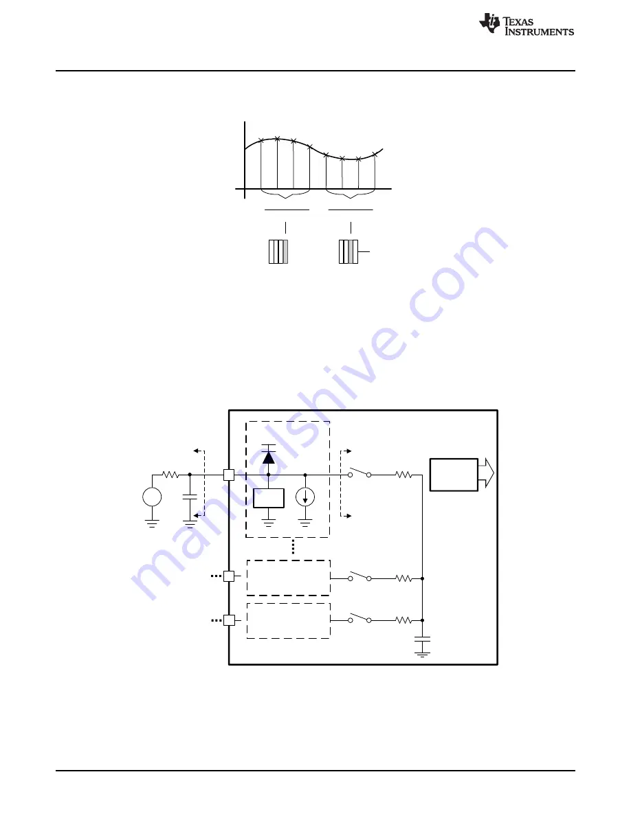
Figure 10-6. Sample Averaging Example
10.3.4 Analog-to-Digital Converter
The Analog-to-Digital Converter (ADC) module uses a Successive Approximation Register (SAR)
architecture to deliver a 12-bit, low-power, high-precision conversion value. The successive approximation
uses a switched capacitor array to perform the dual functions of sampling and holding the signal as well
as providing the 12-bit DAC operation.
shows the ADC input equivalency diagram; for parameter values, see the device-specific data
sheet.
Figure 10-7. ADC Input Equivalency
The ADC operates from both the 3.3-V analog and 1.2-V digital power supplies. The ADC clock can be
configured to reduce power consumption when ADC conversions are not required (see
). The
analog inputs are connected to the ADC through specially balanced input paths to minimize the distortion
and cross-talk on the inputs. Detailed information on the ADC power supplies and analog inputs can be
found in the device-specific data sheet.


