


V
TSENS
2.5 V
1.633 V
0.833 V
Temp
85° C
-40° C
25° C
TSENS
TEMP
55
V
2.7 V
75
§
·
¨
¸
©
¹
0
VREFP - VREFN
V
0xFFF
0x800
- Input Saturation
-(VREFP - VREFN)
Functional Description
713
SLAU723A – October 2017 – Revised October 2018
Copyright © 2017–2018, Texas Instruments Incorporated
Analog-to-Digital Converter (ADC)
Because the maximum peak-to-peak differential signal voltage is 2 × (VREFP – VREFN), the ADC codes
are interpreted as:
mV per ADC code = (2 × (VREFP - VREFN)) / 4096
(6)
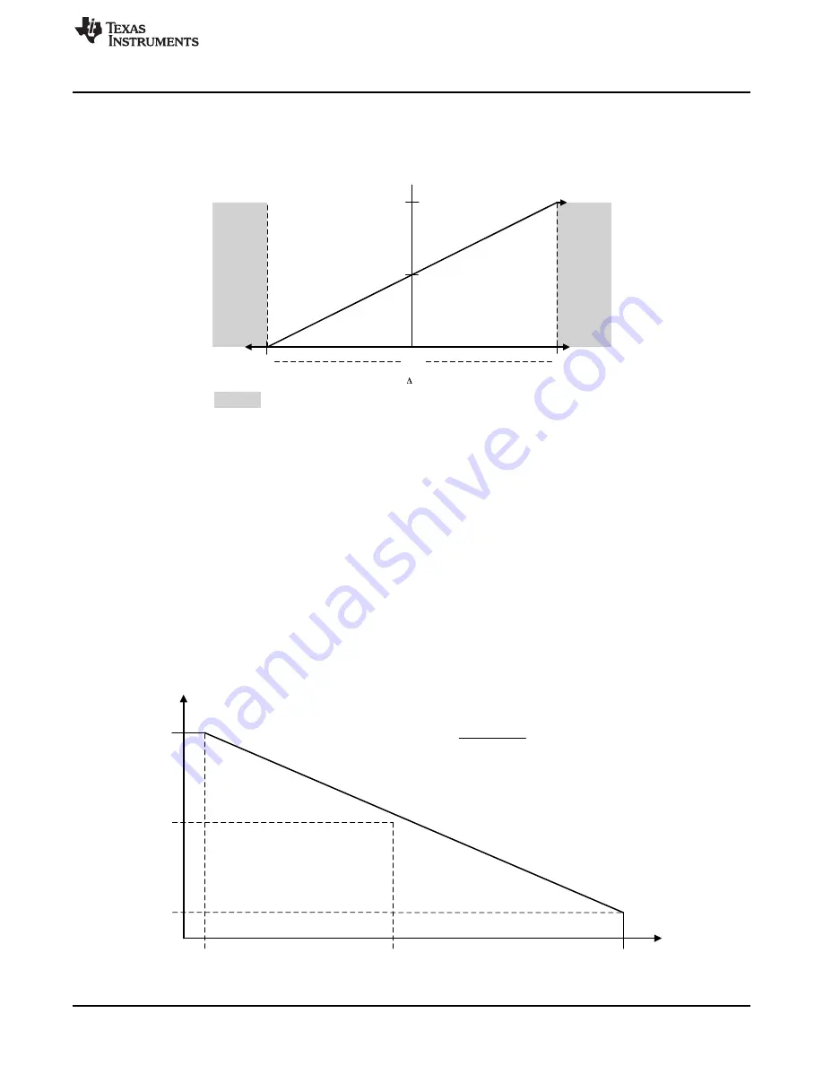
shows how the differential voltage,
∆
V, is represented in ADC codes.
Figure 10-10. Differential Voltage Representation
10.3.6 Internal Temperature Sensor
The temperature sensor serves two primary purposes: 1) to notify the system that internal temperature is
too high or low for reliable operation and 2) to provide temperature measurements for calibration of the
Hibernate module RTC trim value.
The temperature sensor does not have a separate enable, because it also contains the bandgap
reference and must always be enabled. The reference is supplied to other analog modules; not just the
ADC. In addition, the temperature sensor has a second power-down input in the 3.3 V domain which
provides control by the Hibernation module.
The internal temperature sensor converts a temperature measurement into a voltage. This voltage value,
V
TSENS
, is given by the following equation (where TEMP is the temperature in °C):
V
TSENS
= 2.7 – ((TEMP + 55) / 75)
(7)
This relation is shown in
.
Figure 10-11. Internal Temperature Sensor Characteristic


