


ML610Q421/ML610Q422/ML610421 User’s Manual
Chapter 6 Clock Generation Circuit
6 – 5
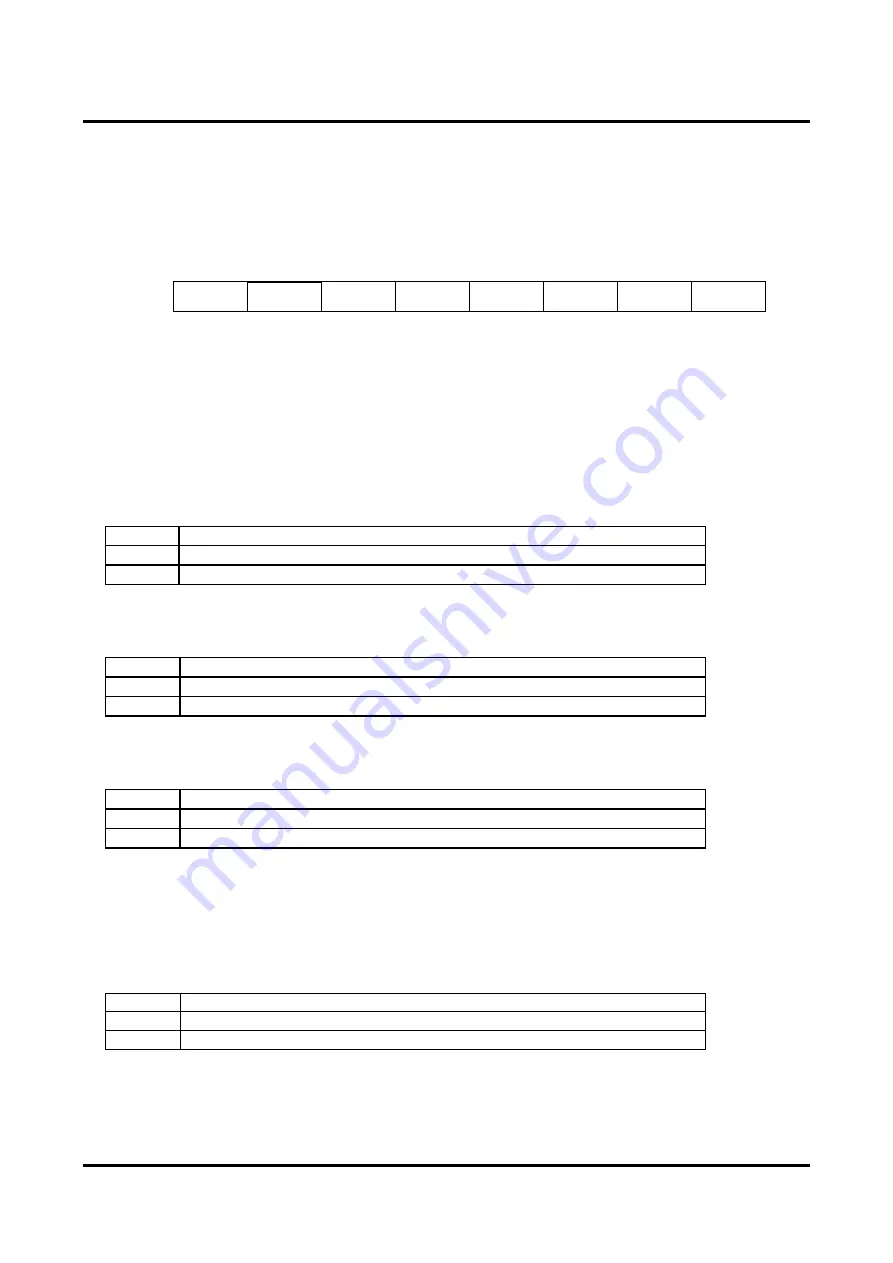
6.2.3
Frequency Control Register 1 (FCON1)
Address: 0F003H
Access: R/W
Access size: 8 bits
Initial value: 03H
7
6
5
4
3
2
1
0
FCON1
LPLL
ENMLT
ENOSC
SYSCLK
R/W
R
R/W
R/W
R/W
R/W
R/W
R/W
R/W
Initial value
0
0
0
0
0
0
1
1
FCON1 is a special function register (SFR) to control the high-speed clock generation circuit and to select system clock.
[Description of Bits]
•
SYSCLK
(bit 0)
The SYSCLK bit is used to select system clock. It allows selection of the low-speed clock (LSCLK) or HSCLK
(1/nOSCLK: n = 1, 2, 4, 8) selected by using the high-speed clock frequency select bit (SYSC1, 0) of FCON0.
When the oscillation of high-speed clock is stopped (ENOSC bit = “0”), the SYSCLK bit is fixed to “0” and the
low-speed clock (LSCLK) is selected for system clock.
SYSCLK
Description
0
LSCLK
1
HSCLK (initial value)
•
ENOSC
(bit 1)
The ENOSC bit is used to select enable/disable of the oscillation of the high-speed clock oscillator.
ENOSC
Description
0
Disables high-speed oscillation
1
Enables high-speed oscillation (initial value)
•
ENMLT
(bit 2)
The ENMLT bit is used to select enable/disable of the operation of the 2
×
low-speed clock (LSCLK
×
2).
ENMLT
Description
0
Disables 2
×
low-speed clock operation (initial value)
1
Enables 2
×
low-speed clock operation
•
LPLL
(bit 7)
The LPLL bit is used as a flag to indicate the oscillation state of PLL oscillation.
When the LPLL bit is set to “1”, this indicates that the PLL oscillation frequency is locked within 8.192 MHz
±
2.5%.
When the LPLL bit is set to “0”, this indicates that the PLL oscillation is inactive or the PLL oscillation frequency is
not within 8.192 MHz
±
2.5%.
LPLL is a read-only bit.
LPLL
Description
0
Disables the use of PLL oscillation (initial value)
1
Enables the use of PLL oscillation
Summary of Contents for ML610421
Page 1: ...ML610Q421 ML610Q422 ML610421 User s Manual Issue Date Feb 9 2015 FEUL610Q421 06...
Page 15: ...Chapter 1 Overview...
Page 44: ...Chapter 2 CPU and Memory Space...
Page 49: ...Chapter 3 Reset Function...
Page 53: ...Chapter 4 MCU Control Function...
Page 69: ...Chapter 5 Interrupts INTs...
Page 93: ...Chapter 6 Clock Generation Circuit...
Page 110: ...Chapter 7 Time Base Counter...
Page 121: ...Chapter 8 Capture...
Page 129: ...Chapter 9 1 kHz Timer 1kHzTM...
Page 135: ...Chapter 10 Timers...
Page 160: ...Chapter 11 PWM...
Page 172: ...Chapter 12 Watchdog Timer...
Page 180: ...Chapter 13 Synchronous Serial Port...
Page 195: ...Chapter 14 UART...
Page 216: ...Chapter 15 I2 C Bus Interface...
Page 231: ...Chapter 16 NMI Pin...
Page 237: ...Chapter 17 Port 0...
Page 246: ...Chapter 18 Port 1...
Page 252: ...Chapter 19 Port 2...
Page 259: ...Chapter 20 Port 3...
Page 270: ...Chapter 21 Port 4...
Page 282: ...Chapter 22 Port A...
Page 290: ...Chapter 23 Melody Driver...
Page 304: ...Chapter 24 RC Oscillation Type A D Converter...
Page 327: ...Chapter 25 Successive Approximation Type A D Converter...
Page 338: ...Chapter 26 LCD Drivers...
Page 371: ...Chapter 27 Battery Level Detector...
Page 378: ...Chapter 28 Power Supply Circuit...
Page 381: ...Chapter 29 On Chip Debug Function...
Page 384: ...Appendixes...
Page 435: ...Revision History...