


Theory of O peration—2440 Service
Transistor Q640 is configured as a shunt-feedback
amplifier with R645, C639, and R639 (C639 and R639 for
instruments with serial numbers B012403 and above) and
C643 (C643 for instruments with serial numbers B012402
and below) as the feedback elements. T he feedback current
through R645 develops a voltage across the resistor that is
positive with respect to ground ( + 1 5 .6 V for instruments
with serial numbers B012402 and below) on the base of the
transistor. The value of this additive voltage plus the diode
drop across CR644 sets the clam ping threshold. Grid Bias
potentiometer R100 varies the voltage across base resistor
divider R642 and R644 and thus sets the feedback current
through R645.
For instruments with
serial
numbers
B 012402 and below, the adjustment range of the pot can set
the nominal clamping level between + 45 V and + 75 V.
When the amplitude of the AC waveform is below the
clamping threshold, diode CR644 will be reverse biased
and the AC waveform will be unclamped. For instruments
with serial numbers B012402 and below, during the time the
diode is reverse biased, transistor Q 640 is kept biased in the
active region by the charge retained on C 643 from the
previous cycle. As the amplitude of the AC waveform at the
junction of CR442 and CR644 exceeds the voltage of C638
(or at the collector of Q 640 for instruments with serial
numbers B012402 and below), diode C R644 becomes
forward biased, and the AC waveform is clam ped at that
level. Any current greater than that required to maintain the
clam p voltage will be shunted to ground ( + 1 5 V supply for
instruments with serial numbers B012402 and below) by
transistor Q640.
Z-AXIS DRIVE LEVEL. The variable Z-Axis signal (VZ)
establishes the lower clam ping level of the AC waveform
applied to the High Voltage Module. When the amplitude of
the waveform drops below the Z-Axis signal level, CR442
becomes forward biased, and the AC waveform is clam ped
to the Z-Axis signal level. The VZ level may vary between
+ 8 V and + 5 0 V, depending on the setting of the
front-panel INTENSITY control.
The AC waveform, now carrying both the grid-bias
information and the Z-Axis drive information, is applied to a
DC Restorer circuit in the High-Voltage Module where it is
lowered to the voltage level of the CRT control grid
(approximately - 2 kV).
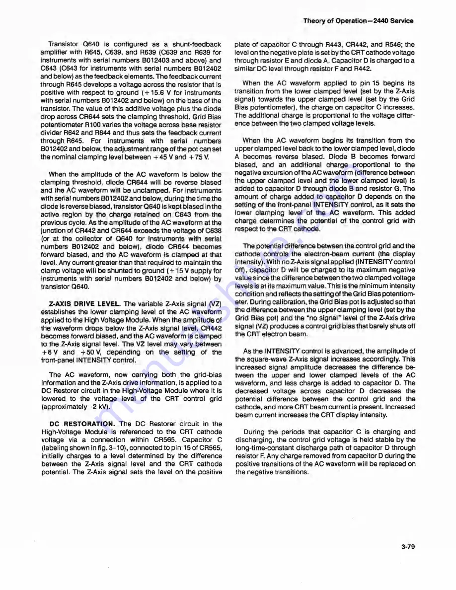
DC RESTO R ATIO N. The DC Restorer circuit in the
High-Voltage Module is referenced to the CRT cathode
voltage via a connection within CR565. Capacitor C
(labeling shown in fig. 3 -1 0 ), connected to pin 15 of CR565,
initially charges to a level determined by the difference
between the Z-Axis signal level and the CRT cathode
potential. The Z-Axis signal sets the level on the positive
plate of capacitor C through R443, CR442, and R546; the
level on the negative plate is set by the CRT cathode voltage
through resistor E and diode A. Capacitor D is charged to a
similar DC level through resistor F and R442.
When the AC waveform applied to pin 15 begins its
transition from the lower clam ped level (set by the Z-Axis
signal) towards the upper clam ped level (set by the Grid
Bias potentiometer), the charge on capacitor C increases.
The additional charge is proportional to the voltage differ
ence between the two clam ped voltage levels.
When the AC waveform begins its transition from the
upper clam ped level back to the lower clam ped level, diode
A becomes reverse biased. Diode B becomes forward
biased, and an additional charge proportional to the
negative excursion of the AC waveform (difference between
the upper clam ped level and the lower clam ped level) is
added to capacitor D through diode B and resistor G. The
amount of charge added to capacitor D depends on the
setting of the front-panel IN TEN SITY control, as it sets the
lower clamping level of the AC waveform. This added
charge determines the potential of the control grid with
respect to the CRT cathode.
The potential difference between the control grid and the
cathode controls the electron-beam current (the display
intensity). With no Z-Axis signal applied (INTENSITY control
off), capacitor D will be charged to its maximum negative
value since the difference between the two clam ped voltage
levels is at its maximum value. This is the minimum intensity
condition and reflects the setting of the Grid Bias potentiom
eter. During calibration, the Grid Bias pot is adjusted so that
the difference between the upper clam ping level (set by the
Grid Bias pot) and the “no signal” level of the Z-Axis drive
signal (VZ) produces a control grid bias that barely shuts off
the CRT electron beam.
As the INTENSITY control is advanced, the amplitude of
the square-wave Z-Axis signal increases accordingly. This
increased signal amplitude decreases the difference be
tween the upper and lower clam ped levels of the AC
waveform, and less charge is added to capacitor D. The
decreased voltage across capacitor D decreases the
potential difference between the control grid and the
cathode, and more CRT beam current is present. Increased
beam current increases the CRT display intensity.
During the periods that capacitor C is charging and
discharging, the control grid voltage is held stable by the
long-time-constant discharge path of capacitor D through
resistor F. Any charge removed from capacitor D during the
positive transitions of the AC waveform will be replaced on
the negative transitions.
3-79
Summary of Contents for 2440
Page 4: ......
Page 12: ......
Page 38: ......
Page 91: ...Theory of Operation 2440 Service 3 49 Figure 3 5 Simplified CCD architecture ...
Page 120: ...Theory of Operation 2440 Service Figure 3 10 DC Restorer 3 78 ...
Page 130: ...Theory of Operation 2440 Service 3 88 ...
Page 136: ...Theory of Operation 2440 Service Figure 3 15 PWM Regulator and Inverter 3 94 ...
Page 138: ...Theory of Operation 2440 Service Figure 3 16 PWM switching waveforms 3 96 ...
Page 208: ......
Page 322: ......
Page 419: ......
Page 423: ...2440 Service Figure 9 4b 2440 Block diagram part 2 6330 27 BLOCK DIAGRAM PART 2 ...
Page 427: ......
Page 428: ...2440 Service WAVEFORMS FOR DIAGRAM 1 6 2 8 5 3 2 ...
Page 429: ......
Page 432: ...2440 Service WAVEFORMS FOR DIAGRAM 2 BUS ISOLATED 6 6 0 3 4 9 ...
Page 433: ...WAVEFORMS FOR DIAGRAM 2 ...
Page 439: ......
Page 445: ......
Page 450: ...2440 Service WAVEFORMS FOR DIAGRAM 8 6603 27 ...
Page 455: ...W A V EFO R M S FOR D IAG RAM 11 WAVEFORMS FOR DIAGRAM 11 6603 29 ...
Page 458: ...WAVEFORMS FOR DIAGRAM 12 ...
Page 463: ...WAVEFORMS FOR DIAGRAM 14 ...
Page 471: ... C N i u i t e x r 4 j u J l i 1 i 6 28 5 44 WAVEFORMS FOR DIAGRAM 18 ...
Page 476: ...WAVEFORMS FOR DIAGRAM 20 ...
Page 490: ...YES ...
Page 492: ......
Page 494: ......
Page 499: ...YES ...
Page 501: ......
Page 502: ...2440 Service FIG 1 C A B IN E T ...
Page 503: ......
Page 510: ...2440 Service SISSVHO Z Old ...
Page 511: ......
Page 512: ...A12 2440 Service F IG 3 C IR C U IT BOARDS ...
Page 513: ......
Page 517: ...10 16 R E V J U L 1993 Replaceable Mechanical Parts ...
Page 518: ...2440 Service ...
Page 519: ...FIG 4 L V H V PWR SUPPLY ...
Page 520: ...FIG 5 ACCESSORIES 2440 Service ...
Page 521: ......
Page 523: ......
Page 529: ......
Page 530: ......
Page 531: ......


