Chapter 10
Miscellaneous Functions
©
National Instruments Corporation
10-9
DAQ-STC Technical Reference Manual
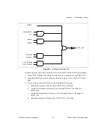
The G_OUT0/RTSI_OUT, OSC, and TEST_IN pins are not included in the internal gate tree.
10.7 Pin Interface
The I/O signals related to the Miscellaneous Functions are listed in the following table. An
asterisk following a pin name indicates that the default polarity for that pin is active low.
Pin Type Notation:
IU
Input, pull up (50 k
Ω
)
O4TU
Output, 4 mA sink, 2.5 mA source tri-state, pull up (50 k
Ω
)
IS
Input, TTL Schmitt trigger
O9TU
Output, 9 mA sink, 5 mA source tri-state, pull up (50 k
Ω
)
O9
Output, 9 mA sink, 5 mA source
PFI8/G_SRC0
PFI9/G_GATE0
G_UP_DOWN0
G_UP_DOWN1
RTSI_TRIGGER0
RTSI_TRIGGER1
RTSI_TRIGGER0
RTSI_TRIGGER1
RTSI_TRIGGER2
RTSI_TRIGGER3
RTSI_TRIGGER2
RTSI_TRIGGER3
RTSI_TRIGGER4
RTSI_TRIGGER5
—
—
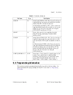
Table 10-3.
Pin Interface
Pin Name
Type
Description
ANALOG_TRIG_DRIVE
O4TU
Analog Trigger Drive—This pin controls whether the
board’s trigger line should be output or input. This bit is
driven directly from a control register on the DAQ-STC.
Related bitfield: Analog_Trigger_Drive.
ANALOG_TRIG_IN_HI
IU
Analog Input Trigger High Voltage Reference—This pin
indicates that the analog trigger waveform has exceeded
the HI voltage reference. Source: This input is typically
fed from an analog comparator on the board.
ANALOG_TRIG_IN_LO
IU
Analog Input Trigger Low Voltage Reference—This pin
indicates that the analog trigger waveform has dropped
below the LOW voltage reference. Source: This input is
typically fed from an analog comparator on the board.
Table 10-2.
Test Mode Input Pin Pairs (Continued)
Pin Pairs
Pin Pairs

