Chapter 3
Analog Output Timing/Control
DAQ-STC Technical Reference Manual
3-74
©
National Instruments Corporation
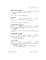
AO_UI_Save_Value
bits: <0..7>
type: Read
in: AO_UI_Save_Registers
address: 16
bits: <0..15>
type: Read
in: AO_UI_Save_Registers
address: 17
This bitfield reflects the contents of the UI counter. Reading from this bitfield while the UI
counter is counting may result in an erroneous value. The eight MSBs are located at the lower
address and the 16 LSBs are located at the higher address.
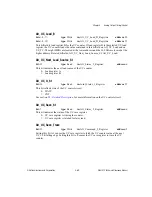
AO_UI_Source_Polarity
bit: 3
type: Write
in: AO_Mode_1_Register
address: 38
This bit selects the active edge of the UI source (the signal that is selected by
AO_UI_Source_Select):
0: Rising edge.
1: Falling edge.
Related bitfields: AI_UI_Source_Select.
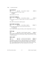
AO_UI_Source_Select
bits: <6..10>
type: Write
in: AO_Mode_1_Register
address: 38
This bitfields selects the UI source:
0: The internal signal AO_IN_TIMEBASE1.
1–10: PFI<0..9>.
11–17: RTSI_TRIGGER<0..6>.
19: The internal signal IN_TIMEBASE2.
31: Logic low.
Related bitfields: AO_UI_Source_Polarity.
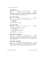
AO_UI_Switch_Load_On_BC_TC
bit: 9
type: Strobe
in: AO_Command_2_Register
address: 5
Setting this bit to 1 causes the UI counter to switch load registers at the next BC_TC. This
action is internally synchronized to the falling edge of the UI_CLK. You can use this bit to
change the update rate during waveform generation at the end of the current MISB. This bit
is cleared automatically.
AO_UI_Switch_Load_On_Stop
bit: 8
type: Strobe
in: AO_Command_2_Register
address: 5
Setting this bit to 1 causes the UI counter to switch load registers upon receiving a STOP
trigger. This action is internally synchronized to the falling edge of the UI_CLK. This bit is
cleared automatically. This bitfield is currently not supported, and it must be set to 0.


