Chapter 3
Analog Output Timing/Control
©
National Instruments Corporation
3-73
DAQ-STC Technical Reference Manual
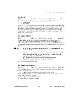
AO_UI_Load_B
bits: <0..7>
type: Write
in: AO_UI_Load_B_Registers
address: 42
bits: <0..15>
type: Write
in: AO_UI_Load_B_Registers
address: 43
This bitfield is load register B for the UI counter. If load register B is the selected UI load
register, the UI counter loads the value contained in this bitfield on AO_UI_Load and on
UI_TC. The eight MSBs are located at the lower address and the 16 LSBs are located at the
higher address. Related bitfields: AO_UI_Next_Load_Source_St, AO_UI_Load.
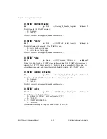
AO_UI_Next_Load_Source_St
bit: 6
type: Read
in: AO_Status_2_Register
address: 6
This bit indicates the next load source of the UI counter:
0: Load register A.
1: Load register B.
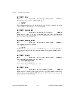
AO_UI_Q_St
bit: 9
type: Read
in: AO_Status_2_Register
address: 6
This field reflects the state of the UI control circuit:
0: WAIT.
1: CNT.
, for more information on the UI control circuit.
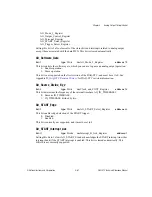
AO_UI_Reload_Mode
bits: <4..6>
type: Write
in: AO_Mode_2_Register
address: 39
This bitfield selects the reload mode for the UI counter:
0: No automatic change of the UI load register.
4: Alternate first period on STOP. Use this setting to make the time interval between
the START trigger and the first UPDATE pulse different from the remaining update
intervals.
5: Switch load register on STOP. Use this setting to synchronously change the update
interval at each STOP.
6: Alternate first period on BC_TC. Use this setting to make the time interval between
the START1 trigger and the first UPDATE pulse different from the remaining
update intervals.
7: Switch load register on BC_TC. Use this setting to synchronously change the update
interval at each BC_TC. This is convenient for staged analog output operation.

