background image

Glossary

DAQ-STC Technical Reference Manual

G-10

©

 National Instruments Corporation

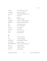
S

s

seconds

S

samples

SC

scan counter

SCAN_IN_PROG

scan in progress signal

SCKG

internal sample clock signal

SCLK

internal update signal

SCLKG

internal sample clock signal

SC_CE

SC count enable signal

SC_CLK

SC clock signal

SC_GATE

SC counter gate signal

SC_HOLD

SC hold signal 

SC_LOAD

SC load signal

SC_LOAD_SRC

SC load source signal

SC_SRC

SC source signal

SC_START1

START1 signal synchronized to SC_RC

SC_TC

SC counter TC signal

SCXI

Signal Conditioning eXtensions for Instrumentation

SEC_IRQ_OUT_BANK0

secondary interrupt output for interrupt group A

SEC_IRQ_OUT_BANK1

secondary interrupt output for interrupt group B

SEL<0..4>

select signal, channels 0 through 4

SHIFTIN

data shift pulse signal

SI

24-bit scan interval counter

Summary of Contents for DAQ-STC Series

Page 1: ...DAQ DAQ STC Technical Reference Manual System Timing Controller for Data Acquisition DAQ STC Technical Reference Manual January 1999 Edition Part Number 340934B 01...

Page 2: ...36 Canada Ontario 905 785 0085 Canada Qu bec 514 694 8521 Denmark 45 76 26 00 Finland 09 725 725 11 France 01 48 14 24 24 Germany 089 741 31 30 Hong Kong 2645 3186 Israel 03 6120092 Italy 02 413091 Ja...

Page 3: ...UCTS OR INCIDENTAL OR CONSEQUENTIAL DAMAGES EVEN IF ADVISED OF THE POSSIBILITY THEREOF This limitation of the liability of National Instruments will apply regardless of the form of action whether in c...

Page 4: ...Programming the AITM 2 1 2 2 Features 2 2 2 3 Simplified Model 2 4 2 4 Analog Input Functions 2 6 2 4 1 Low Level Timing and Control 2 6 2 4 1 1 ADC Control 2 7 2 4 1 2 Data FIFO Control 2 7 2 4 1 3 C...

Page 5: ...2 33 2 6 3 10 Start of Scan 2 34 2 6 3 11 End of Scan 2 37 2 6 3 12 Convert Signal 2 38 2 6 3 13 Enable Interrupts 2 40 2 6 3 14 Arming 2 41 2 6 3 15 Starting the Acquisition 2 41 2 6 3 16 Analog Inpu...

Page 6: ...put Counters 2 123 2 8 3 1 SC Counter 2 124 2 8 3 2 SC Control 2 124 2 8 3 3 SI Counter 2 126 2 8 3 4 SI Control 2 126 2 8 3 5 SI2 Counter 2 127 2 8 3 6 SI2 Control 2 127 2 8 3 7 DIV Counter 2 128 2 8...

Page 7: ...6 1 2 Resetting 3 21 3 6 1 3 Board Power up Initialization 3 22 3 6 1 4 Trigger Signals 3 23 3 6 1 5 Number of Buffers 3 24 3 6 1 6 Update Selection 3 26 3 6 1 7 Channel Select 3 28 3 6 1 8 LDAC Sourc...

Page 8: ...ut Timing 3 86 3 7 3 CPU Driven Analog Output Timing 3 88 3 7 4 DAQ STC and CPU Driven Analog Output Timing 3 90 3 7 5 Secondary Analog Output Timing 3 93 3 7 6 Decoded Signal Timing 3 94 3 7 7 Local...

Page 9: ...ncumulative Event Counting 4 4 4 4 1 4 Buffered Cumulative Event Counting 4 5 4 4 1 5 Relative Position Sensing 4 6 4 4 2 Time Measurement 4 6 4 4 2 1 Single Period Measurement 4 6 4 4 2 2 Single Puls...

Page 10: ...nabling the General Purpose Counter Timer Output Pin 4 35 4 6 2 Bitfield Descriptions 4 35 4 7 Timing Diagrams 4 53 4 7 1 CTRSRC Minimum Period and Minimum Pulsewidth 4 55 4 7 2 CTRSRC to CTROUT Delay...

Page 11: ...ative Position Sensing 4 75 4 8 11 6 Single Period Measurement 4 76 4 8 11 7 Single Pulsewidth Measurement 4 77 4 8 11 8 Buffered Period Measurement 4 78 4 8 11 9 Buffered Semiperiod Measurement 4 79...

Page 12: ...O 7 5 7 5 Pin Interface 7 6 7 6 Programming Information 7 7 7 6 1 Windowed Mode Register Access Example 7 7 7 6 2 Programming the Digital Interface 7 8 7 6 2 1 Parallel Digital I O 7 9 7 6 2 2 Hardwa...

Page 13: ...s 9 1 9 2 1 Pin Interface 9 1 9 3 Programming Information 9 3 9 3 1 Programming the Write Strobes 9 4 9 3 2 Bitfield Descriptions 9 4 9 4 Timing Diagrams 9 5 Chapter 10 Miscellaneous Functions 10 1 Ov...

Page 14: ...Multiplexer Control 2 9 Figure 2 6 Internal CONVERT Timing 2 10 Figure 2 7 External CONVERT Timing 2 11 Figure 2 8 Internal START 2 12 Figure 2 9 External START 2 13 Figure 2 10 SI Special Trigger Del...

Page 15: ...2 35 SCAN_IN_PROG Deassertion 2 103 Figure 2 36 STOP Delay Synchronous Mode 2 104 Figure 2 37 STOP Delay Asynchronous Mode 2 104 Figure 2 38 SC_TC Delay 2 105 Figure 2 39 SI_TC Delay 2 105 Figure 2 4...

Page 16: ...e Internal UPDATE Mode 3 103 Figure 3 27 External Trigger Synchronous Level External UPDATE Mode 3 103 Figure 3 28 External Trigger Synchronous Edge External UPDATE Mode 3 103 Figure 3 29 START1 Delay...

Page 17: ...igure 4 28 CTR_U D Setup Timing Internal Timing Mode 4 60 Figure 4 29 CTR_U D Setup Timing External Timing Mode 4 60 Figure 4 30 General Purpose Counter Timer Model 4 61 Figure 4 31 G_SOURCE Generatio...

Page 18: ...Interface 2 19 Table 2 2 CONVERT_SRC Reference Pin Selection 2 84 Table 2 3 Basic Analog Input Timing 2 86 Table 2 4 Configuration Memory Timing 2 90 Table 2 5 External Analog Input Timing 2 96 Table...

Page 19: ...Gate Actions 4 67 Table 4 16 START STOP Modes for Edge Gating 4 68 Table 4 17 Reload on G_CONTROL Selections 4 68 Table 4 18 Gate Interrupts 4 69 Table 4 19 PFI Selectors 4 70 Table 5 1 Pin Interface...

Page 20: ...xxi DAQ STC Technical Reference Manual Table B 1 DAQ STC Registers B 1 Table B 2 Registers in Order of Address B 5 Table B 3 Bitfield Description Guide B 9 Table C 1 DAQ STC Pins in Alphabetical Order...

Page 21: ...er level programmer manual you can refer directly to the DAQ STC Technical Reference Manual Programmers should have to read only the Programming Information section of each chapter in order to program...

Page 22: ...us Functions discusses the miscellaneous functions not covered in the other chapters The miscellaneous functions include clock distribution the programmable frequency output analog triggering and test...

Page 23: ...h advises you of precautions to take to avoid being electrically shocked bold Bold text denotes the names of menu items or dialog box buttons or options bold italic Bold italic text denotes a note cau...

Page 24: ...Use these manuals for hardware installation and configuration instructions specification information about your DAQ hardware and application hints Software manuals Examples of software manuals you ma...

Page 25: ...mputers Customer Communication National Instruments wants to receive your comments on our products and manuals We are interested in the applications you develop with our products and we want to help i...

Page 26: ...control signals to independent A D and D A subsystems Two counters in the general purpose counter timer module implement event counting time measurement and pulse generation functions and supply timin...

Page 27: ...ows the primary components of an analog input subsystem On an analog input board a sample hold circuit samples the analog value of one or more input channels and an A D converter ADC converts the anal...

Page 28: ...retransmit signal for the configuration FIFO and monitors the FIFO empty flag The ghost signal from the configuration FIFO inhibits the AI data FIFO clock to provide a multirate sampling capability T...

Page 29: ...ions 1 2 DAQ STC Block Diagram Figure 1 3 shows a block diagram of the DAQ STC The diagram shows all of the I O signals as well as the direction of the signal input output or bidirectional Each chapte...

Page 30: ...nals RTSI_TRIGGER 0 6 or other internal signals This chapter presents a list of the AITM features followed by a simplified model that introduces a few AITM related signals an overview of each of the A...

Page 31: ...um sample rate of 10 MS s Maximum interval of 3 3 ms between channels with 50 ns resolution External timing for the following signals START START1 START2 CONVERT SI source with special considerations...

Page 32: ...Cs in the pretrigger mode Gating Hardware and software gating Seamless interface to the configuration FIFO and the data FIFO Error detection Overrun and overflow error detection flags for internal or...

Page 33: ...g Input Waveform The primary analog input timing signal is the CONVERT pulse which instructs the ADC to begin a conversion on the selected analog input channel CONVERT pulses are organized into groups...

Page 34: ...rated by the ADC SOC indicates that a conversion has begun and EOC indicates that a conversion is complete Using CONVERT as a reference the output circuit generates several ancillary signals used on t...

Page 35: ...acquisition The START1 trigger signal begins the acquisition sequence and may come from one of several sources PFI RTSI software or general purpose counter 0 2 4 Analog Input Functions The AITM is a h...

Page 36: ...vent loss of data at high speeds and to increase bus bandwidth The data FIFO control signals support such a FIFO The SHIFTIN signal loads the result of each conversion into the data FIFO Three status...

Page 37: ...ernal multiplexer Typically analog input boards are limited to eight or 16 input channels An external multiplexer overcomes this limitation by time division multiplexing several analog signals onto ea...

Page 38: ...n 2 4 2 Scan Level Timing and Control for more information on the START trigger The STOP trigger which asserts after the appropriate number of conversions usually comes from the configuration FIFO A s...

Page 39: ...les the STST_GATE External CONVERT pulses that occur when the STST_GATE is enabled pass through the DAQ STC External CONVERT pulses that occur when the STST_GATE is disabled are blocked Timing for the...

Page 40: ...ART mode or the PFI selector external START mode 2 4 2 1 Internal START Mode In the internal START mode the SI_TC SI counter TC signal becomes the START pulse The START1 trigger causes the SI counter...

Page 41: ...ecognize external START pulses Each external START initiates a scan causing the DAQ STC to generate CONVERT pulses until a STOP is received If the external START pulses occur at a rate higher than the...

Page 42: ...ernal START pulses for a fixed time period after the START1 trigger Software can program the SI counter to count edges on the internal IN_TIMEBASE signal for an absolute time delay or it can program t...

Page 43: ...nd terminates the acquisition upon completion of the programmed number of scans Posttrigger acquisitions can be retriggerable or nonretriggerable In the retriggerable mode additional START1 pulses tha...

Page 44: ...sition sequence with a pretrigger count requirement of four scans and a posttrigger scan requirement of three scans The total number of scans acquired before START2 occurs is six because the START2 tr...

Page 45: ...whenever you need DAQ devices with multiple DAQ STC ASICs to acquire data in a synchronized manner that is when multiple ASICs share the same START1 and START2 triggers With master slave triggering o...

Page 46: ...and the location of the third scan had it not been gated off Figure 2 13 Free Run Gating Mode 2 4 4 2 Halt Gating Mode Halt gating mode is available only when the START signal is generated internally...

Page 47: ...rnal gate Figure 2 14 Halt Gating Mode 2 4 5 Single Wire Mode In the single wire mode one signal is used as both an external START and an external CONVERT Interval scan timing is still permitted altho...

Page 48: ...to generate the FIFO interrupt and the FIFO request signal AIFREQ based on the status of the FIFO The input polarity is selectable and the input state can be directly observed in one of the status re...

Page 49: ...Dedicated STOP Output This output reflects the state of the active high internal STOP signal The hardware generates AI_STOP_OUT and the internal STOP signal by passing the output of the STOP selector...

Page 50: ...switch to the next entry in the external scan list Two output modes are available for the EXTMUX_CLK output In the first mode EXTMUX_CLK trails the LOCALMUX_CLK pulse by 0 5 1 5 AI_OUT_TIMEBASE perio...

Page 51: ...channel in the scan list Output polarity is selectable Destination Configuration FIFO Options Active Low Active High Ground High Z Related bitfields AI_LOCALMUX_CLK_Output_Select AI_LOCALMUX_CLK_Puls...

Page 52: ...nable SHIFTIN O9TU Data Shift Pulse This output sends ADC data over the serial link The serial link transfers data serially across the RTSI bus but is not currently supported The signal is similar to...

Page 53: ...Each pair of registers is treated as a single bitfield in this document 2 6 1 Register and Bitfield Programming Considerations Several write only registers on the DAQ STC contain bitfields that contr...

Page 54: ...Register Make sure that the interrupt does not disturb the Window_Address_Register during this sensitive period disable interrupts during windowed mode accesses or write the interrupt routines so that...

Page 55: ...r some single tasking operating systems such as DOS the directives Begin critical section and End critical section directly map to CLI and STI assembly language instructions respectively However other...

Page 56: ...tate You can then program the AITM for any desired operation 2 6 3 2 Board Power up Initialization Part of the AITM programming depends only on properties of the hardware surrounding the DAQ STC If yo...

Page 57: ...AI_SHIFTIN_Polarity 0 active low or 1 active high AI_SHIFTIN_Pulse_Width 0 0 5 1 5 AI_OUT_TIMEBASE periods or 1 1 5 2 AI_OUT_TIMEBASE periods AI_EOC_Polarity 0 rising edge or 1 falling edge AI_SOC_Pol...

Page 58: ...or an SCXI device The major distinction between power up initialization and environment setup is that power up initialization is always the same for a device using the DAQ STC while the latter enviro...

Page 59: ...2 6 3 5 FIFO Request Use this function to select the data FIFO condition on which interrupt or DMA requests will be generated Function FIFO_Request_Selection Begin critical section AI_Configuration_S...

Page 60: ...te and then start your application If you only want to use the software gate configure the hardware gate as indicated in section 2 6 3 6 Hardware Gate Programming with the following changes to the set...

Page 61: ...field AI_START1_Pulse or 1 through 10 PFI 0 9 or 11 through 17 RTSI_TRIGGER 0 6 or 18 the G_OUT signal from general purpose counter 0 If AI_START1_Select is 0 then AI_START1_Polarity 0 AI_START1_Edge...

Page 62: ...onfiguration_End 1 End critical section 2 6 3 9 Number of Scans Use this function to select the number of scans to be acquired In a staged acquisition the number of scans to be executed in each stage...

Page 63: ...select the scan start event You can specify the scan rate by choosing an internally generated periodic signal to be the START signal In a staged acquisition the number of clocks between START in each...

Page 64: ...delay from the START1 trigger to the first start of scan by preloading SI AI_SI_Load_A number of clocks from START1 to first START 1 AI_SI_Initial_Load_Source 0 AI_SI_Load 1 AI_SI_Load_A number of clo...

Page 65: ...NVERT have the same polarity then AI_START_Select 1 through 10 PFI 0 9 or 11 through 17 RTSI_TRIGGER 0 6 or 18 bitfield AI_START_Pulse or 19 the G_OUT signal from general purpose counter 0 AI_START_Sy...

Page 66: ...e 0 AI_SI_Switch_Load_On_SC_TC 1 si_last_load_register B Else si_last_load_register A AI_Configuration_End 1 End critical section 2 6 3 11 End of Scan Use this function to select the end of scan event...

Page 67: ...an one channel per scan then DIV counter is used as the STOP source AI_STOP_Select 0 DIV_TC AI_STOP_Sync 1 AI_STOP_Edge 0 AI_STOP_Polarity 0 AI_DIV_Load_A number of channels per scan 1 AI_DIV_Load 1 E...

Page 68: ...t all or you are using SI and it uses IN_TIMEBASE2 AI_SI2_Source_Select 0 same signal selected as SI source AI_SI_Source_Select 19 IN_TIMEBASE2 AI_SI_Source_Polarity 0 Else You want to use SI2 and you...

Page 69: ...tion of the AI_Convert_Signal function the SC_GATE is selected The SC_GATE enables the external CONVERT pulses whenever the SC counter is enabled to count and blocks the external CONVERT pulses whenev...

Page 70: ...1 AI_End_On_End_Of_Scan 1 If internal START mode OR SI special trigger delay will be used then arm_si 1 Else arm_si 0 If internal CONVERT mode then arm_si2 1 Else arm_si2 0 AI_SC_Arm 1 You must set th...

Page 71: ...ll AI_Reset_All Call AI_Board_Personalize Call AI_Initialize_Configuration_Memory_Output Call AI_Board_Environmentalize Call AI_FIFO_Request_Selection Call AI_Hardware_Gating Call AI_Trigger_Signals C...

Page 72: ...indicates the current position in the array You can use the following function to change the scan rate Function AI_Scan_Rate_Change If acquisition is not retriggerable OR you will change the scan rat...

Page 73: ...1 The number of clocks for the first two posttrigger acquisition sequences is programmed in the AI_Scan_Start function The variable si_last_load_register indicates which load register was accessed mo...

Page 74: ..._pointer 1 si_last_load_register 0 AI_SC_TC_Interrupt_Ack 1 Check for interrupt latency problems If AI_SC_TC_Error_St is 0 then AI_SC_TC_Error_Confirm 1 Else Inform user that an SC_TC error has occurr...

Page 75: ...am is part of a system in which interrupts do not exist you can use programming sequences intended for ISRs directly in your application coupled with the programming technique known as polling If you...

Page 76: ...T_Interrupt_Ack STOP To enable AI_STOP_Interrupt_Enable and AI_START_Interrupt_Enable To recognize AI_STOP_St To acknowledge and clear AI_STOP_Interrupt_Ack START1 To enable AI_START1_Interrupt_Enable...

Page 77: ...s with contiguous locations within a register can belong to a bitfield The high and low pairs of load and save registers for 24 bit counters are also treated as bitfields The AITM related bitfields ar...

Page 78: ...that no spurious glitches appear on the output pins and on the internal circuit components If you do not set this bit to 1 the DAQ STC may behave erroneously This bit is cleared by setting AI_Configur...

Page 79: ...selects the polarity of the PFI2 CONV output signal if enabled for output 0 Active low 1 Ground 2 Active low 3 Active high Related bitfields BD_2_Pin_Dir AI_CONVERT_Pulse bit 0 type Strobe in AI_Comm...

Page 80: ...e signal that is selected by AI_CONVERT_Source_Select 0 Falling edge 1 Rising edge You must set this bit to 0 in the internal CONVERT mode Related bitfields AI_CONVERT_Source_Select AI_CONVERT_Source_...

Page 81: ...ternal CONVERT 1 START synchronizes to SC_SRC Since the clock SC_SRC is internally delayed relative to SI2_SRC and FSCLK setting this bit to 1 provides additional margin for the external START to reac...

Page 82: ...V counter The DIV counter loads the value contained in this bitfield on AI_DIV_Load and on DIV_TC Related Bitfields AI_DIV_Load AI_DIV_Q_St bit 13 type Read in AI_Status_2_Register address 5 This bit...

Page 83: ...n This bit is useful for device diagnostic applications Related bitfields AI_EOC_Polarity AI_Error_Interrupt_Ack bit 13 type Strobe in Interrupt_A_Ack_Register address 2 Setting this bit to 1 clears A...

Page 84: ...high enables operation 1 Active low low enables operation AI_External_Gate_Select bits 0 4 type Write in AI_Mode_3_Register address 87 This bitfield enables and selects the external gate 0 External ga...

Page 85: ..._CLK pulses that will correspond to one LOCALMUX_CLK pulse AI_EXTMUX_CLK_Output_Select bits 6 7 type Write in AI_Output_Control_Register address 60 This bit enables and selects polarity for the EXTMUX...

Page 86: ...ags input signals AIFFF AIFHF AIFEF and MUXFEF 0 Active low 1 Active high Related bitfields AI_FIFO_Empty_St AI_FIFO_Full_St AI_FIFO_Half_Full_St AI_Config_Memory_Empty_St AI_FIFO_Full_St bit 14 type...

Page 87: ...O interrupt on FIFO full Keep the request and interrupt asserted while the FIFO is full 3 Generate DMA request and FIFO interrupt on FIFO more than half full Keep the request and interrupt asserted wh...

Page 88: ...nternal CONVERT mode if you select IN_TIMEBASE2 as the SI2 source For this reason you must not rely on this bit as an end of acquisition indicator AI_LOCALMUX_CLK_Output_Select bits 4 5 type Write in...

Page 89: ...ll AI data FIFO that is the reading from the FIFO is too slow to match the writing to the FIFO If the overflow error occurs at least one point of data has been lost This bit is cleared by setting AI_E...

Page 90: ...n state The resetable registers are AI_Command_1_Register AI_Command_2_Register AI_Mode_1_Register AI_Mode_2_Register AI_Mode_3_Register AI_Output_Control_Register AI_Personal_Register AI_START_STOP_S...

Page 91: ...C_Arm_St AI_Disarm AI_SC_Armed_St bit 0 type Read in AI_Status_2_Register address 5 This bit indicates whether the SC counter is armed 0 Disarmed 1 Armed Related bitfields AI_SC_Arm AI_SC_Gate_Enable...

Page 92: ..._Registers address 19 This bitfield is load register A for the SC counter If load register A is the selected SC load register the SC counter loads the value contained in this bitfield on AI_SC_Load an...

Page 93: ...er address 5 This bit indicates the status of the SC save register 0 SC save register is tracing the counter 1 SC save register is latched for later read Related bitfields AI_SC_Save_Trace AI_SC_Save_...

Page 94: ...ck is not set between two SC TCs This allows you to detect large interrupt latencies and potential problems associated with them To clear this bit set SC_TC_Error_Confirm to 1 Related bitfields AI_SC_...

Page 95: ...interrupt in the secondary interrupt bank 0 Disabled 1 Enabled SC_TC interrupts are generated on every SC_TC falling edge unless the pretrigger acquisition mode is selected In the pretrigger acquisiti...

Page 96: ...and AI_FIFO_SHIFTIN pulses occurs immediately after the active edge of EOC AI_SI_Arm bit 10 type Strobe in AI_Command_1_Register address 8 Setting this bit to 1 arms the SI counter The counter remain...

Page 97: ...field is load register A for the SI counter If load register A is the selected SI load register the SI counter loads the value contained in this bitfield on AI_SI_Load and on SI_TC The eight MSBs are...

Page 98: ...nge the sample interval at each STOP 6 Alternate first period on every SC_TC Use this setting to make the interval between the START1 trigger and the first scan different from the scan interval 7 Swit...

Page 99: ...Do not set this bit to 1 in the internal START mode AI_SI_Switch_Load_On_SC_TC bit 9 type Strobe in AI_Command_2_Register address 4 Setting this bit to 1 causes the SI counter to switch load registers...

Page 100: ...bit indicates whether the SI2 counter is armed 0 Disarmed 1 Armed Related bitfields AI_SI2_Arm AI_SI2_Initial_Load_Source bit 9 type Write in AI_Mode_2_Register address 13 This bit selects the initia...

Page 101: ...8 9 type Read in Joint_Status_1_Register address 27 This bitfield reflects the state of the SI2 control circuit 0 WAIT 1 1 CNT 2 WAIT 2 See section 2 8 Detailed Description for more information on th...

Page 102: ...Status_2_Register address 29 This bit reflects the state of the SOC pin after the polarity selection This bit is useful for device diagnostic applications Related bitfields AI_SOC_Polarity AI_Software...

Page 103: ...The START interrupt is generated on valid START triggers received by the DAQ STC A valid START trigger is one that is received while the SC counter is enabled to count AI_START_Output_Select bit 10 t...

Page 104: ...hile the SC counter is enabled to count AI_START_Select bits 0 4 type Write in AI_START_STOP_Select_Register address 62 This bit selects the START trigger 0 The internal signal SI_TC 1 10 PFI 0 9 11 1...

Page 105: ...ields AI_Start_Stop_Gate_St AI_Start_Stop_Gate_St bit 5 type Read in Joint_Status_1_Register address 27 This bit indicates the status of the start stop gate if start stop gating is enabled 0 External...

Page 106: ...automatically Related bitfields AI_START1_St AI_START1_Interrupt_Enable bit 1 type Write in Interrupt_A_Enable_Register address 73 This bit enables the START1 interrupt 0 Disabled 1 Enabled The START1...

Page 107: ...ated bitfields AI_START1_Pulse AI_START1_St bit 7 type Read in AI_Status_1_Register address 2 This bit indicates that a valid START1 trigger has been received by the DAQ STC 0 No 1 Yes A valid START1...

Page 108: ...AI_START2_St AI_START2_Interrupt_Enable AI_START2_Interrupt_Enable bit 2 type Write in Interrupt_A_Enable_Register address 73 This bit enables the START2 interrupt 0 Disabled 1 Enabled The START2 inte...

Page 109: ...Pulse AI_START2_St bit 8 type Read in AI_Status_1_Register address 2 This bit indicates whether a valid START2 trigger has been received by the SC counter in the pretrigger acquisition mode 0 No 1 Yes...

Page 110: ...pt_Enable bit 4 type Write in Interrupt_A_Enable_Register address 73 This bit enables the STOP interrupt 0 Disabled 1 Enabled The STOP interrupt is generated on valid STOP triggers recognized by the D...

Page 111: ...7 11 type Write in AI_START_STOP_Select_Register address 62 This bitfield selects the STOP trigger 0 The internal signal DIV_TC or bitfield AI_STOP_Pulse 1 10 PFI 0 9 11 17 RTSI_TRIGGER 0 6 18 The int...

Page 112: ...ectional pin PFI7 AI_START when the pin is configured to output the internal signal AD_START 0 Output the normal internal version of the signal 1 Pulse stretch the internal signal to be 1 2 AI_OUT_TIM...

Page 113: ...is section refers to pin to pin timing Because many of the timing parameter definitions are based on internal signals and the internal signals can be selected from a variety of sources this section de...

Page 114: ...is set for divide by two operation each edge of OUT_CLK represents a rising edge of OSC or RTSI_OSC Otherwise OUT_CLK and OSC or RTSI_OSC are identical 11 17 RTSI_TRIGGER 0 6 19 The CONVERT source is...

Page 115: ...signals is shown in Figure 2 16 Figure 2 16 Basic Analog Input Timing Table 2 3 Basic Analog Input Timing Name Description Minimum Maximum Tcconv CONVERT_SRC to CONVERT internal convert 19 58 CONVERT_...

Page 116: ...uld be detected in just the interval labeled A or in both intervals A and B You should include the B region in the overrun detection for ADCs that tri state or otherwise output invalid data after the...

Page 117: ...etransmit or a FIFO reset The AIFREQ signal is based on these FIFO flags as well as on the last TC of the SC counter AIFREQ can be configured internally to generate interrupt requests refer to AI_FIFO...

Page 118: ...source clock period The LOCALMUX_CLK signal reads the next word of data from the configuration memory and is asserted by the CONVERT signal When an external multiplexer is being used the LOCALMUX_CLK...

Page 119: ...nal is asserted by the leading edge of CONVERT and is held for either two or four output clock edges regardless of polarity and then until the active edge of SOC Table 2 4 Configuration Memory Timing...

Page 120: ...EF indicates that the configuration memory has been emptied and should be reset The LOCALMUX_FFRT signal is asserted on the trailing edge of the LOCALMUX_CLK signal and is deasserted after one or two...

Page 121: ...are driven by CONVERT_SRC In the internal CONVERT mode CONVERT_SRC is equal to OSC or RTSI_OSC In the external CONVERT mode CONVERT_SRC is selected to be one of the PFI 0 9 or RTSI_TRIGGER 0 6 inputs...

Page 122: ...and recognition circuitry The edge sensitive mode generates an intermediate internal signal by prelatching the external signal at its active edge This intermediate signal is routed to the latching and...

Page 123: ...Figure 2 21 External Trigger Timing Asynchronous Level Figure 2 22 External Trigger Timing Asynchronous Edge CONVERT_SRC START1 START2 START STOP Ts_strt1 Th_strt1 Th_strt2 Th_strt Th_stop Ts_strt2 Ts...

Page 124: ...gger Timing Synchronous Level Internal CONVERT Mode Figure 2 24 External Trigger Timing Synchronous Edge Internal CONVERT Mode SI2 Source START1 START2 START STOP Ts_strt1 Th_strt1 Th_strt2 Th_strt Th...

Page 125: ...inimum Maximum Ts_strt1 START1 setup to CONVERT_SRC 33 36 Tstrt1 START1 pulsewidth edge mode 6 Th_strt1 START1 hold from CONVERT_SRC level mode 4 Ts_strt2 START2 setup to CONVERT_SRC 31 34 Tstrt2 STAR...

Page 126: ...y RTSI output Timing for START1 and START2 depends on whether you select synchronous mode or asynchronous mode using AI_START1_Sync and AI_START2_Sync Synchronous Mode When you select synchronous mode...

Page 127: ...of CONVERT_SRC that recognizes the external trigger generates the output Figure 2 29 shows the propagation delays for START1 Figure 2 30 shows the propagation delays for START2 Figure 2 29 START1 Del...

Page 128: ...gure 2 31 shows the propagation delays for START1 Figure 2 32 shows the propagation delays for START2 Figure 2 31 START1 Delays Asynchronous Mode Table 2 6 START1 and START2 Timing Synchronous Mode Na...

Page 129: ...SCAN_IN_PROG pin PFI7 AI_START or on the RTSI_BRD 2 3 outputs The timing for START and SCAN_IN_PROG depends on whether you select internal CONVERT or external CONVERT using AI_CONVERT_Source_Select Th...

Page 130: ...the propagation delays for START and SCAN_IN_PROG in the internal CONVERT mode Figure 2 33 START Delays Internal CONVERT Name Description Minimum Maximum Tpfi SI2 Source to PFI output START 14 56 Tbrd...

Page 131: ...ART and SCAN_IN_PROG in the external CONVERT mode The deassertion delay for PFI7 AI_START is indicated for the case where AI_Trigger_Length is set to 0 Figure 2 34 START Delays External CONVERT Name D...

Page 132: ...that occurs while STOP and DIV_TC are both asserted Figure 2 35 shows the behavior of the SCAN_IN_PROG outputs during deassertion Figure 2 35 SCAN_IN_PROG Deassertion 2 7 8 4 STOP Trigger You can out...

Page 133: ...In asynchronous mode the STOP outputs follow the external trigger Figure 2 37 shows the behavior of the STOP outputs in asynchronous mode Figure 2 37 STOP Delay Asynchronous Mode Name Description Mini...

Page 134: ...C In external CONVERT mode the SC source is a delayed version of the external CONVERT source For this reason SC_TC has additional delay in external CONVERT mode Figure 2 38 SC_TC Delay 2 7 9 2 SI_TC F...

Page 135: ...mode provides pseudosimultaneous operation in which a group of channels is sampled at one rate and the sampling of channels within a group occurs at another rate The timing for this mode is shown in F...

Page 136: ...elected mode of operation The START trigger enables a particular scan and is generated by either an external signal or the internal signal SI_TC refer to AI_START_Select The SI counter is started by t...

Page 137: ...tware strobe refer to AI_STOP_Select The external signal must meet the setup and pulsewidth requirements indicated in section 2 7 7 External Triggers in order to guarantee recognition by the AITM Alth...

Page 138: ...s controlled by either an external gate signal or a software strobe Timing for the external gate depends on whether you select internal CONVERT or external CONVERT using AI_CONVERT_Source_Select In in...

Page 139: ...Run Gating Mode Timing External CONVERT The shaded areas in Figures 2 42 and 2 43 indicate where those signals would be asserted had they not been gated off The recognition of the external gate signa...

Page 140: ...falling edge and used on the rising edge but it must be recognized prior to or at the same source clock edge as the SI counter counting down to zero The SI counter stops at one and remains there unti...

Page 141: ...e counters the primary logic blocks are the counter control blocks the routing logic block the interrupt control block and the output control block Figure 2 45 AITM Block Diagram AI_IN_TIMEBASE1 IN_TI...

Page 142: ...ave Synchronization This signal is generated by the hardware by passing the output of the AI_START1 selector through polarity selection edge detection and synchronization synchronized to FSC_SRC bypas...

Page 143: ...el in the onboard mux gain list has been generated so that LOCALMUX_CLK can be asserted to switch to the next channel When an external multiplexer is not being used AI_External_MUX_Present 0 DIV_TC ca...

Page 144: ...sing the load command When the counter is armed SC_CLK is the same as SC_SRC Related bitfields AI_SC_Load SC_GATE SC Counter Gate This signal is generated by the SC control logic SC_GATE conditions th...

Page 145: ...se for the SC and DIV counters In the internal CONVERT mode SC_SRC is the same signal as SI2_SRC In the external CONVERT mode SC_SRC is equal to SCLK The external trigger and gate inputs which are not...

Page 146: ...the counter can be loaded using the load command When the counter is armed SI_CLK is the same as SI_SRC Related bitfields AI_SI_Load SI_HOLD SI Hold This signal controls the SI save register If SI_HO...

Page 147: ...e synchronized to FSC_SRC Related bitfields AI_START_Select AI_START_Pulse AI_START_Edge AI_START_Sync START1 Start 1 This signal is the start trigger signal for the SC SI SI2 and DIV counters START1...

Page 148: ...stop mode it halts CONVERT generation until the next START This is accomplished by stopping the SI2 counter at the next sample pulse if an internal CONVERT is used or by clearing the STST_GATE at the...

Page 149: ...0 6 MOUT MOUT VDD POLARITY ACK EDGE EOUT D Q R 20 to 1 MUX SEL 0 4 NOTE Does not show all possible selections SYNC OUT ACK EXT_TIMING INT_CLK EXT_CLK DELAY EXT_TIMING INT_CLK DELAY_EXT_CLK D Q R D Q...

Page 150: ...0 9 RTSI 0 6 GND AI_SI_Source AI_TB1 PFI 0 9 RTSI 0 6 TB2 GND AI_CONVERT_Source SI2_TC PFI 0 9 RTSI 0 6 GOUT0 GND AI_START_Source SI_TC PFI 0 9 RTSI 0 6 SW GOUT0 GND AI_STOP_Source DIV_TC SW PFI 0 9 R...

Page 151: ...START1_Sync AI_START1_Edge and AI_START1_Polarity are the options for selection of START1 synchronization edge detection and polarity START1 is always external and should be edge detected and synchron...

Page 152: ...an interval Software stores the scan interval in SI load register B and the delay from START1 in SI load register A The SI counter initially loads from load register A and then the SI load source is s...

Page 153: ...to AI_SC_Save The SC save register latch signal deasserts after a rising and then a falling edge of SC_SRC following a 0 being written to AI_SC_Save 2 8 3 2 SC Control The SC counter is controlled by...

Page 154: ...SC counter is armed AI_SC_Arm TRANS is high and EXT_GATE is enabled The SC disarm signal SC_DISARM clears the AI_SC_Arm bit in the register map SC_DISARM asserts on the transition from the CNT state t...

Page 155: ...SC_TC switch load registers on the next STOP switch load registers on the next SI_TC The term alternate load registers refers to the action of having one load from the secondary load register and the...

Page 156: ...eload_Mode option allows the SI2 counter to alternate load registers once after every STOP The SI2 control circuit generates the count enable signals 2 8 3 6 SI2 Control The SI2 counter is controlled...

Page 157: ...high Figure 2 51 SI2 Control Circuit State Transitions 2 8 3 7 DIV Counter The DIV counter is a 16 bit down counter The DIV counter typically divides down LOCALMUX_CLK when an external multiplexer is...

Page 158: ...l SCKG controls the count operation of the DIV counter When the internal timebase is selected for the SC source AI_CONVERT_Source_Select is set to 0 SCKG becomes the sample interval counter TC signal...
Page 159: ...the STOP interrupt to operate properly the START interrupt must also be enabled and operating In addition the START interrupt must be acknowledged prior to the assertion of the STOP signal in order f...

Page 160: ...After a valid START the actual interrupt signal appears on the active edge of SC_CLK Note that this interrupt must be used in conjunction with the START interrupt START1 interrupt Interrupts are gene...

Page 161: ...n overflow error occurs when an attempt is made to write the ADC result to a full AI data FIFO In hardware this is detected when a SHIFTIN pulse occurs while the AI FIFO full flag AIFFF is active This...

Page 162: ...ce or output clocks all of the others must use the indicated clock source These are only the nominal pulsewidths the actual synchronization edges and propagation delays are detailed in section 2 7 Tim...

Page 163: ...update mode It also controls the number of DAC writes generated in an update cycle The secondary update group contains a 16 bit secondary update interval counter UI2 which generates an independent up...

Page 164: ...own counter Maximum update rate of 1 6 MHz on two output channels Maximum frequency of 20 MHz yields 50 ns resolution with a maximum interval of 0 83 s Divide by two timebase yields 100 ns resolution...

Page 165: ...trigger Interval counters have alternate first period capability for retriggerable delay from trigger Minimum delay of 1 update interval clock Maximum delay of 224 update interval clocks Gating Hardw...

Page 166: ...source for the UPDATE pulse may come from the UI counter internal UPDATE source or the select circuit external UPDATE source Using UPDATE as a reference the output section generates several ancillary...

Page 167: ...sources such as PFI RTSI software and the internal signal START1 from the AITM 3 4 Analog Output Functions The basic analog output functionality provided by the DAQ STC is the timing of up to 16 inde...

Page 168: ...igure 3 2 DAQ STC Driven Analog Output 3 4 1 2 CPU Driven Analog Output The DAQ STC also provides circuitry that allows the CPU to write directly to the output channels The primary signals for CPU dri...

Page 169: ...ossibility exists that the CPU and DAQ STC will both attempt to write to the DACs at the same time The CPU is given priority over the DAQ STC but it can not interrupt a DAQ STC write cycle in progress...

Page 170: ...TC supports several methods for transferring analog output data from computer memory to the DACs In CPU driven analog output the CPU writes the output data directly to the DACs In DAQ STC driven analo...

Page 171: ...he data FIFO and the FIFO contents are repeated a number of times The AOFEF signal notifies the DAQ STC that the data FIFO is empty and the AOFFRT signal instructs the data FIFO to retransmit its data...

Page 172: ...ignal TMRDACWR indicating that data is required for a DAC write operation The assertion of TMRDACREQ initiates a transfer across the data link Once the transfer completes the AOFEF signal is released...

Page 173: ...C writes output data to the first three DACs Figure 3 8 Unbuffered Data Interface 3 4 4 Update Timing for Primary Group Analog Output In DAQ STC driven analog output the UPDATE signal allows DACs for...

Page 174: ...Figure 3 10 shows a sequence of externally timed UPDATE pulses and indicates the delay from START1 to the first UPDATE Figure 3 10 External UPDATE Timing 3 4 5 Buffer Timing and Control for Primary A...

Page 175: ...e to the first buffer in the nonretriggerable single buffer mode Figure 3 11 shows an example of the nonretriggerable single buffer mode The buffer contains five data points so the UC counter is progr...

Page 176: ...ATE mode because the UI counter can be programmed with a new value for each MISB Also note that the DAQ STC defines the UPDATE interval to last from the beginning of the current UPDATE to the beginnin...

Page 177: ...how mute buffers can be used to introduce pauses in the analog output timing In the example a single buffer containing two points is repeated twice generating four update pulses A mute buffer is then...

Page 178: ...hat pin is active low Pin Type Notation IU Input pull up 50 k O4TU Output 4 mA sink 2 5 mA source tri state pull up 50 k O9TU Output 9 mA sink 5 mA source tri state pull up 50 k Table 3 1 Pin Interfac...

Page 179: ...FO Retransmit This active low output instructs the data FIFO to retransmit its contents It is used primarily in the local buffer mode When enabled AOFFRT pulses each time AOFEF indicates a FIFO empty...

Page 180: ...lsewidth is selectable Destination DACs Related Bitfields AO_TMRDACWR_Pulse_Width DACWR 0 1 O4TU DAC Write Strobes These pins serve as write strobes for DACs combining the TMRDACWR and CPUDACWR signal...

Page 181: ...rated by the DAQ STC whenever data from the data FIFO needs to be written to the DACs Following each UPDATE the TMRDACWR signal pulses a number of times to load data into the DACs according to the num...

Page 182: ...order the character marks the boundary between two groups of assignments that have to be executed sequentially For example in the following pseudocode the first bitfield assignment must be performed f...

Page 183: ...directives Begin critical section and End critical section directly map to CLI and STI instructions respectively However other operating systems may require specific primitives to achieve this functi...

Page 184: ...1 AO_Error_Interrupt_Ack 1 AO_Configuration_End 1 End critical section Perform the AO_Board_Personalize programming function in order to bring the primary AO module of DAQ STC into a known state You...

Page 185: ...ctive high AO_DMA_PIO_Control 0 FIFO data interface mode or 1 unbuffered data interface mode AO_AOFREQ_Enable 0 disabled or 1 enabled AO_AOFREQ_Polarity 0 active high or 1 active low AO_TMRDACWR_Pulse...

Page 186: ...of points in the buffer and the number of buffer iterations If you are using the local buffer mode with mute buffers this function will set the part of the delay parameters that correspond to the num...

Page 187: ...A uc_new_ticks 0 1 AO_Mute_B new_mute_flag 1 AO_BC_Load_B bc_new_ticks 1 1 AO_UC_Load_B uc_new_ticks 1 1 AO_BC_Reload_Mode 1 AO_UC_Switch_Load_Every_BC_TC 1 ao_tick_count_to_use 2 ao_last_load_registe...

Page 188: ...section 3 6 1 6 Update Selection Use this function to select the update event You can specify an update rate by choosing an internally generated periodic event For waveform staging operation in the i...

Page 189: ...UI_Load 1 AO_UI_Load_B ui_new_ticks 1 1 AO_UI_Relaod_Mode 7 Else AO_UI_Initial_Load_Source 0 AO_UI_Reload_Mode 0 If there is no special delay from START1 to first update then AO_UI_Load_A number of cl...

Page 190: ...the BC_GATE enables the external UPDATE pulses whenever the BC counter is enabled to count and blocks the external UPDATE pulses whenever the BC counter is not enabled to count The BC_GATE must be dis...

Page 191: ...d update mode AO_Configuration_End 1 End critical section 3 6 1 9 Stop On Error Use this function to set the error conditions upon which the AOTM will stop Function AO_Errors_To_Stop_On Begin critical...

Page 192: ...1 generate interrupt AO_BC_TC_Interrupt_Enable 0 no interrupt or 1 generate interrupt AO_UC_TC_Interrupt_Enable 0 no interrupt or 1 generate interrupt AO_START1_Interrupt_Enable 0 no interrupt or 1 g...

Page 193: ...does not do anything Function AO_Start_The_Generation Begin critical section If software trigger then AO_START1_Pulse 1 End critical section 3 6 1 14 Primary Analog Output Program Use the following se...

Page 194: ...stage If the interrupt cannot be serviced during one MISB of the waveform the DAQ STC will not be programmed properly for the next MISB To avoid this you should keep interrupt latency and workload on...

Page 195: ...sr 1 If ao_shut_down_isr is 1 then AO_End_On_BC_TC 1 ao_tick_count_to_use 0 new_bc_ticks bc_new_ticks ao_tick_count_to_use new_uc_ticks uc_new_ticks ao_tick_count_to_use new_ui_ticks ui_new_ticks ao_t...

Page 196: ...back on track 3 6 3 Changing Update Rate during an Output Operation for Primary Analog Output Group Use this function to change the update rate during an output operation if you are not performing wav...

Page 197: ...STCs for synchronized analog output operation To do this use the RTSI connection to connect the trigger signal to the trigger input of the master DAQ STC Also connect the output equivalent of the trig...

Page 198: ...owever your system will be devoted entirely to one application Information on interrupts and polling can be found in the National Instruments Application Note 010 Programming Interrupts for Data Acqui...

Page 199: ...IFO_Half_Full_St and AO_FIFO_Empty_St To clear You must change the FIFO state by dealing with the FIFO UPDATE To enable AO_UPDATE_Interrupt_Enable To recognize AO_UPDATE_ST To clear AO_UPDATE_Interrup...

Page 200: ...s section discusses programming for the secondary group Refer to section 3 6 1 Programming for a Primary Analog Output Operation for a discussion of the primary group 3 6 6 2 Resetting Assume the seco...

Page 201: ...selected by AO_UPDATE2_Pulse_Width or 1 selected by AO_UPDATE2_Original_Pulse AO_UPDATE2_Pulse_Width 0 3 3 5 AO_OUT_TIMEBASE periods or 1 1 1 5 AO_OUT_TIMEBASE periods AO_UPDATE2_Original_Pulse 0 equa...

Page 202: ...ing The variable ao2_tick_count_to_use introduced in this function will be used later in the waveform staging AO2_Staged_ISR function Function AO2_Counting Begin critical section Declare variable ao2_...

Page 203: ..._UI2_Source_Polarity 0 rising edge or 1 falling edge AO_UI2_Initial_Load_Source A AO_UI2_Load_A number of clocks between each update 1 AO_UI2_Load 1 If waveform staging then AO_UI2_Load_B ui2_ticks 0...

Page 204: ...Interrupts can normally be serviced after some delay commonly referred to as interrupt latency In some cases the interrupt latency may be long enough to cause problems in your waveform stage If the i...

Page 205: ...rm_Disarm 0 Else new_ticks ui2_ticks ao2_tick_count_to_use If new_ticks is 0 ao2_shut_down_isr ao2_shut_down_isr 1 Else ao2_tick_count_to_use ao2_tick_count_to_use 1 If ao2_last_load_register is A the...

Page 206: ...eration if you are not performing waveform staging The variable ao2_last_load_register keeps track of which load register should be used This variable was introduced in the AO2_Updating function Funct...

Page 207: ...information on programming group B interrupts 3 6 11 Bitfield Descriptions Bits in the register bit maps are organized into bitfields A bitfield can contain one or more bits Only bits with contiguous...

Page 208: ...nd_1_Register address 9 This bit arms the BC counter The counter remains armed and the bit remains set until it is disarmed either by hardware or by setting AO_Disarm to 1 Related bitfields AO_BC_Arme...

Page 209: ...the BC counter with the contents of the selected BC load register If the BC counter is armed writing to this bit has no effect This bit is cleared automatically Related bitfields AO_BC_Arm AO_BC_Init...

Page 210: ...n AO_Mode_2_Register address 39 This bit selects the reload mode for the BC counter 0 No automatic change of the BC load register 1 The BC counter will switch load registers on BC_TC You can use setti...

Page 211: ...t this bit to 1 Setting 0 is not currently supported AO_BC_Switch_Load_On_TC bit 4 type Strobe in AO_Command_2_Register address 5 Setting this bit to 1 causes the BC counter to switch load registers a...

Page 212: ...AO_BC_TC_Second_Irq_Enable bit 0 type Write in Second_Irq_B_Enable_Register address 76 This bit enables the BC_TC interrupt in the secondary interrupt bank 0 Disabled 1 Enabled BC_TC interrupts are ge...

Page 213: ...rs AO_Configuration_Start which holds the analog output circuitry in reset to prevent glitches on the output pins during configuration You should set this bit to 1 at the end of the configuration proc...

Page 214: ...put signals 0 Immediate update mode LDACi outputs an inverted version of the DAC write signals TMRDACWR and CPUDACWR 1 Timed update mode LDACi outputs the UPDATE or UPDATE2 signal See AO_LDACi _Source...

Page 215: ...lly synchronized to the falling edge of the UC source This bit is cleared automatically Related bitfields AO_Continuous AO_End_On_UC_TC bit 14 type Strobe in AO_Command_2_Register address 5 Setting th...

Page 216: ...See Appendix D DAQ STC Revision History for DAQ STC revision information AO_External_Gate_Polarity bit 3 type Write in AO_Output_Control_Register address 86 This bit selects the polarity of the prima...

Page 217: ...Until the end of CPUDACWR 1 Until the start of CPUDACWR Select option 0 for slow CPU interfaces and option 1 for fast CPU interfaces Note This bit also determines how long the DAQ STC deasserts CHRDY_...

Page 218: ...in AO_Status_1_Register address 3 This bit reflects the state of the AOFHF input signal after the polarity selection which indicates the data FIFO status 0 Half full or less 1 More than half full Rela...

Page 219: ...1 Asserted AO_FIFO_Mode selects the condition on which to generate the DMA request and FIFO interrupt Related bitfields AO_FIFO_Mode AO_FIFO_Retransmit_Enable bit 13 type Write in AO_Mode_2_Register a...

Page 220: ...i_Update_Mode AO_Multiple_Channels bit 5 type Write in AO_Mode_1_Register address 38 This bit enables multiple output channel support 0 Disabled 1 Enabled Related bitfields AO_Number_Of_Channels AO_Mu...

Page 221: ...UPDATE pulses DAC address lines AO_ADDR 0 3 will also be affected if appropriate You should use this bit during the AO configuration phase in the programming sequence to load the first point of the b...

Page 222: ...t_Divide_By_2 bit 5 type Write in Clock_and_FOUT_Register address 56 This bit determines the frequency of the internal timebase AO_OUT_TIMEBASE 0 Same as IN_TIMEBASE 1 IN_TIMEBASE divided by 2 AO_Over...

Page 223: ...the first revision of the DAQ STC and must be set to 0 See Appendix D DAQ STC Revision History for DAQ STC revision information AO_Source_Divide_By_2 bit 4 type Write in Clock_and_FOUT_Register addre...

Page 224: ...Command_1_Register address 9 Setting this bit to 1 sends a START trigger to the counters if the START software strobe is selected AO_START_Select is set to 0 This bit is cleared automatically This bit...

Page 225: ...Register address 27 This bit indicates the status of the start stop gate if start stop gating is enabled 0 Inactive gate 1 Active gate This bit is currently not supported and its setting is undefined...

Page 226: ...sed bitfields AO_START1_St AO_START1_Interrupt_Enable bit 1 type Write in Interrupt_B_Enable_Register address 75 This bit enables the START1 interrupt 0 Disabled 1 Enabled The START1 interrupt is gene...

Page 227: ...ART1_St bit 8 type Read in AO_Status_1_Register address 3 This bit indicates that a valid START1 trigger has been received by the DAQ STC 0 No 1 Yes A valid START1 trigger is one that is received whil...

Page 228: ...when a BC_TC trigger error occurs 0 Continue on BC_TC trigger error 1 Stop on BC_TC trigger error AO_BC_TC_Trigger_Error_St will be set in either case Related bitfields AO_BC_TC_Trigger_Error_St AO_St...

Page 229: ...us_2_Register address 29 This bit indicates whether the TMRDACWR sequence initiated by an UPDATE or by setting AO_Not_An_UPDATE to 1 has completed 0 Completed 1 n progress You can poll this bit if you...

Page 230: ...e_2_Register address 39 If the UC counter is disarmed this bit selects the initial UC load register 0 Load register A 1 Load register B If the UC counter is armed writing to this bit has no effect Rel...

Page 231: ...5 type Read in AO_Status_2_Register address 6 This bit indicates the next load source of the UC counter 0 Load register A 1 Load register B AO_UC_Q_St bit 14 type Read in Joint_Status_1_Register addre...

Page 232: ...bit 2 type Write in AO_Mode_1_Register address 38 This bit enables the UC counter to switch load register on UC_TC 0 Disabled 1 Enabled AO_UC_Switch_Load_On_BC_TC bit 6 type Strobe in AO_Command_2_Re...

Page 233: ...AO_Status_1_Register address 3 This bit indicates whether the UC counter has reached TC 0 No 1 Yes To clear this bit set AO_UC_TC_Interrupt_Ack to 1 Related bitfields AO_UC_TC_Interrupt_Ack Refer to T...

Page 234: ...gister A 1 Load register B If the UI counter is armed writing to this bit has no effect Related bitfields AO_UI_Arm AO_UI_Load bit 9 type Strobe in AO_Command_1_Register address 9 If the UI counter is...

Page 235: ...in AO_Status_2_Register address 6 This field reflects the state of the UI control circuit 0 WAIT 1 CNT See section 3 8 Detailed Description for more information on the UI control circuit AO_UI_Reload_...

Page 236: ...in AO_Mode_1_Register address 38 This bitfields selects the UI source 0 The internal signal AO_IN_TIMEBASE1 1 10 PFI 0 9 11 17 RTSI_TRIGGER 0 6 19 The internal signal IN_TIMEBASE2 31 Logic low Relate...

Page 237: ...AO_UI2_Armed_St bit 11 type Read in AO_Status_2_Register address 6 This bit indicates whether the UI2 counter is armed 0 Disarmed 1 Armed AO_UI2_Configuration_End bit 10 type Strobe in Joint_Reset_Re...

Page 238: ...0 Active high high enables counting 1 Active low low enables counting AO_UI2_External_Gate_Select bits 7 11 type Write in AO_START_Select_Register address 66 This bit selects the secondary external ga...

Page 239: ...I2_Load AO_UI2_Load_B bits 0 15 type Write in AO_UI2_Load_B_Register address 55 This bitfield is load register B for the UI2 counter If load register B is the selected UI2 load register the UI2 counte...

Page 240: ...AO_UI2_Source_Select bits 7 11 type Write in AO_Trigger_Select_Register address 67 This bit selects the UI2 source 0 The internal signal AO_IN_TIMBASE1 1 10 PFI 0 9 11 17 RTSI_TRIGGER 0 6 18 The inter...

Page 241: ...interrupt request in either interrupt bank if the UI2_TC interrupt is enabled This bit is cleared automatically Related bitfields AO_UI2_TC_St AO_UI2_TC_Interrupt_Enable bit 7 type Write in Interrupt...

Page 242: ...dress 86 This bit enables and selects the polarity of the UPDATE2 output signal 0 High Z 1 Ground 2 Enable active low 3 Enable active high AO_UPDATE2_Output_Toggle bit 2 type Write in AO_Output_Contro...

Page 243: ...iginal_Pulse is 0 this bitfield setting determines the maximal pulsewidth of the UPDATE2 signal so that the pulsewidth is equal to the shorter of this pulsewidth and the original signal pulsewidth The...

Page 244: ..._UPDATE_Source_Select AO_UPDATE_Output_Select bits 0 1 type Write in AO_Output_Control_Register address 86 This bitfield enables and selects the polarity of the UPDATE output signal 0 High Z 1 Ground...

Page 245: ...ginal_Pulse is 0 this bit determines the maximum pulsewidth of the UPDATE and PFI5 UPDATE signals so that the pulsewidth is equal to the shorter of this pulsewidth and the original signal pulsewidth T...

Page 246: ...rd Related subsections within the chip can be programmed to operate at different clock rates and the necessary synchronization time can significantly affect the edges and pulsewidths of the board leve...

Page 247: ...rence pin is determined by AI_UI_Source_Select 1 10 PFI 0 9 11 17 RTSI_TRIGGER 0 6 19 The UPDATE source is selected to be the output of general purpose counter 1 The reference pin is determined by G1_...

Page 248: ...ure 3 14 shows the timing for these signals in a basic analog output sequence There are two UPDATE signals shown UPDATE SRC and UPDATE OUT The UPDATE signal can be operated from either the source or o...

Page 249: ...urce clocks 1 1 Toup UPDATE pulsewidth output clocks 1 3 1 5 3 5 Tcd OUT_CLK to UPDATE deasserted 12 28 Tupwr UPDATE to TMRDACWR asserted 0 5 1 5 Tctwr OUT_CLK to TMRDACWR asserted 11 34 Tctreq OUT_CL...

Page 250: ...The primary output signals are CHRDY_OUT CPUDACWR and AO_ADDR 0 3 and the input signals are CPUDACREQ and the bus addresses A 1 4 The CPUDACREQ signal notifies the DAQ STC that a CPU write to a DAC i...

Page 251: ..._CLK to CPUDACWR asserted 14 15 43 47 Tcwr CPUDACWR pulsewidth 2 3 2 3 Tccwrd OUT_CLK to CPUDACWR deasserted 14 12 44 37 Tas AO_ADDR 0 3 setup to CPUDACWR 2 3 5 9 Tah AO_ADDR 0 3 hold from CPUDACWR 2...

Page 252: ...ion of the CPUDACREQ signal and the assertion of the CPUDACWR signal is between 0 5 and 1 5 clock periods The signal CPUDACWR can be programmed to two or three output clock periods which is an exact n...

Page 253: ...tely after the falling edge of the output clock so the DAQ STC continued with its own write cycle Each write slot is separated by one clock period as shown in the timing diagram The two signals CPUDAC...

Page 254: ...while the DAQ STC driven write will be delayed as shown in Figure 3 17 The shaded region of the signal TMRDACWR indicates where the TMRDACWR signal would have been asserted had there been no contentio...

Page 255: ...this signal Figure 3 18 Secondary Analog Output Timing The numbers in parentheses indicate the number of clock periods that occur at the minimum and maximum delays because those parameters are clock...

Page 256: ...TMRDACWR or CPUDACWR This allows the DACs to immediately update to their new values In the timed update mode LDACi is a multiplexer which selects between UPDATE and UPDATE2 This allows the DAC group t...

Page 257: ...easserted 1 5 Twrld CPU TMRDACWR to LDACi asserted 4 0 TwrldN CPU TMRDACWR to LDACi deasserted 4 2 Tckwr OUT_CLK to DACWRi asserted 15 47 TckwrN OUT_CLK to DACWRi deasserted 12 37 Taddr TMRDACWR to da...

Page 258: ...ffer is repeated a number of times The primary signals are UPDATE TMRDACWR AO_ADDR 0 3 AOFFRT and AOFEF The UPDATE TMRDACWR and AO_ADDR 0 3 signals operate identically to the basic analog output case...

Page 259: ...ssertion of AOFFRT which is deasserted on the next rising edge of the output clock Name Description Minimum Maximum Tcup UPDATE_SRC to UPDATE asserted 18 56 Tsup UPDATE SRC pulsewidth 1 1 Toup UPDATE...

Page 260: ...on could simply use the CPU driven examples given above but this wastes the host CPU resources The DAQ STC provides a DMA mode of operation where the FIFOs can be omitted Due to the pinout restriction...

Page 261: ...TE OUT deasserted 12 38 Tctwr OUT_CLK to TMRDACWR asserted 11 34 Tlwrd last CPUDACWR to TMRDACWR deasserted 2 6 Treqrdy AOFEF to CHRDY_OUT asserted 4 12 Twrrdy CPUDACWR to CHRDY_OUT deasserted 4 2 11...

Page 262: ...alog output The CPUDACWR signal is used to actually write the DMA data to the DACs The TMRDACWR signal will remain asserted until the completion of the last CPUDACWR The AOFFF input is the DMA acknowl...

Page 263: ...g output occurs when back to back updates are programmed via the counter timer In the above example the shortest pulsewidths for each signal have been selected The UPDATE pulse is one output clock per...

Page 264: ...ace along with software strobes The secondary analog output module consists of the single counter UI2 This 16 bit counter begins counting immediately after it is armed by software Software can also st...

Page 265: ...Internal UPDATE Mode Figure 3 26 External Trigger Synchronous Edge Internal UPDATE Mode Figure 3 27 External Trigger Synchronous Level External UPDATE Mode Figure 3 28 External Trigger Synchronous Edg...

Page 266: ...gger depends on whether you select synchronous mode or asynchronous mode using AO_START1_Sync Synchronous Mode When you select synchronous mode for START1 the timing depends on whether you select inte...

Page 267: ...ual Figure 3 29 START1 Delays Synchronous Mode Internal UPDATE Name Description Minimum Maximum Tpfi Source to PFI output 9 37 Trtsi Source to RTSI output 11 43 Tbrd Source to BRD output 16 60 All tim...

Page 268: ...ure 3 30 START1 Delays Synchronous Mode External UPDATE Asynchronous Mode When you select asynchronous mode for START1 the external trigger itself generates the rising edge of the output Figure 3 31 s...

Page 269: ...the BC_TC and UC_TC outputs 3 7 12 1 BC_TC Figure 3 32 shows the delays associated with the BC_TC signal Figure 3 32 BC_TC Delay Name Description Minimum Maximum Tpfi Trigger to PFI output 9 34 Trtsi...

Page 270: ...ters in the DAQ STC register map See Appendix B Register Information for more information on the register addresses containing these bitfields Figure 3 34 shows a block diagram of the AOTM The AOTM co...

Page 271: ..._TC AO_IN_TIMEBASE1 IN_TIMEBASE2 PFI 0 9 AOFREQ CPUDACWR AO_ADDR 0 3 UPDATE UPDATE2 AOFEF AOFHF START1 STOP UI2_SRC UI_SRC BC_SRC EXT_GATE EXT_GATE2 RTSI_TRIGGER 0 6 START1 STOP BC_TC BC_SRC UC_TC EXT...

Page 272: ...ter If BC_HOLD 0 the BC save register tracks the BC counter output If BC_HOLD 1 the BC save register latches the BC counter output Related bitfields AO_BC_Save_Trace BC_LOAD BC Load This signal pulses...

Page 273: ...hronization EXT_GATE External Gate The external gate can be used to gate the UPDATE output It is selectable from either polarity of PFI 0 9 or from RTSI_TRIGGER 0 6 Related bitfields AO_External_Gate_...

Page 274: ...ART1_Polarity STOP Stop This signal terminates the buffer in progress It is the same signal as UC_TC UC_CE UC Count Enable This signal enables and disables the UC counter Refer to Figure 3 38 for the...

Page 275: ...nd_1_Register so that the counter can be loaded using the load command When the counter is armed UI_CLK is the same as UI_SRC UI_DISARM UI Disarm This signal which is generated by the UI control circu...

Page 276: ...AO_Command_1_Register so that the counter can be loaded using the load command When the counter is armed UI2_CLK is the same as UI2_SRC UI2_LOAD UI2 Load This signal pulses to load the value from the...

Page 277: ...selector Table 3 7 PFI Selectors MUX 0 1 10 11 17 18 19 20 31 AO_START1_Source SW PFI 0 9 RTSI 0 6 AI_ST1 GND AO_START_Source SW UC_TC PFI 0 9 RTSI 0 6 GND AO_UPDATE_Source UI_TC PFI 0 9 RTSI 0 6 GOU...

Page 278: ...correct timing and need not be synchronized Software strobes do not have the correct timing and should always be synchronized Synchronization of external signals results in a one half bit synchroniza...

Page 279: ...the UC and BC control blocks respectively 3 8 3 1 UI Counter The UI counter is a 24 bit down counter with dual load registers The UI counter typically counts the interval between UPDATEs as well as t...

Page 280: ...urning to the WAIT state Figure 3 37 UI Control Circuit State Transitions 3 8 3 3 UC Counter The UC counter is a 24 bit down counter with dual load registers and output save latch The UC counter typic...

Page 281: ...e until the counter is armed and a START1 pulse is received When these two events occur the control circuit moves to the CNT state and the counter begins counting On UC_TC the control circuit either r...

Page 282: ...nd to switch load registers on the next BC_TC The BC control circuit generates the count enable signals The BC save register latch signal asserts after a rising and then a falling edge of BC_SRC follo...

Page 283: ...counter is disarmed AO_UI2_Load will load the counter with the value from the selected load register During normal operation the UI2 counter will synchronously reload from the selected load register...

Page 284: ...UPDATE command is issued to a DAC that was not loaded with data In hardware this is detected when an UPDATE pulse occurs before all of the TMRDACWR pulses from the previous UPDATE have completed The T...

Page 285: ...ce are not written in the allotted time The error detection circuit is armed on the last BC_TC of the waveform staging sequence If a software clear AO_BC_TC_Interrupt_Ack does not occur before the nex...

Page 286: ...so pulses to update the DAC 3 8 7 Nominal Signal Pulsewidths Table 3 9 lists the nominal pulsewidths for the signals associated with analog input Notice that only the UPDATE and UPDATE2 signals can us...

Page 287: ...lect the GPCT input signals from any of the 17 external timing I O pins on the DAQ STC Ten of these PFI lines are user programmable I O pins and are available on the I O connector of the MIO E Series...

Page 288: ...e information Interevent relative time stamping Two sets of save registers to save the counter value via an external control signal or via software command Current count value can be read without affe...

Page 289: ...s until they can be read by software 4 4 Counter Timer Functions The purpose of the GPCT is to provide counter timer functions that are improved over those available on the Am9513 based DAQ boards thr...

Page 290: ...ess is gated that is halted and resumed via G_GATE When G_GATE is active the counter counts pulses that occur on the G_SOURCE signal after the software arm When G_GATE is inactive the counter retains...

Page 291: ...4 Buffered Noncumulative Event Counting 4 4 1 4 Buffered Cumulative Event Counting Buffered cumulative event counting is similar to simple event counting except that the G_GATE signal indicates when...

Page 292: ...time by asynchronously reading the counter value Figure 4 6 shows an example of relative position sensing Figure 4 6 Relative Position Sensing 4 4 2 Time Measurement In the time measurement functions...

Page 293: ...e HW save register latches the counter value for software read Figure 4 8 shows a single pulsewidth measurement where the pulsewidth of G_GATE is five G_SOURCE rising edges Figure 4 8 Single Pulsewidt...

Page 294: ..._GATE input counting the number of rising edges that occur on G_SOURCE while G_GATE remains in an active and in an inactive state At the completion of each semiperiod interval for G_GATE the HW save r...

Page 295: ...the pulse generation functions the counter generates a single pulse of specified duration following the software arm The software arm occurs when software sets the counter arm bit in the DAQ STC regi...

Page 296: ...r to generate a single pulse with programmable delay and programmable pulsewidth You should specify the programmable parameters in terms of periods of the G_SOURCE input Single triggered pulse generat...

Page 297: ...4 14 shows the generation of two pulses with a pulse delay of five and a pulsewidth of three Figure 4 14 Retriggerable Single Pulse Generation 4 4 3 4 Buffered Retriggerable Single Pulse Generation Th...

Page 298: ...lses only after the active gate edge occurs The hardware provides an alternate output mode so that G_OUT outputs two counter TC pulses instead of a single long pulse 4 4 4 1 Continuous Pulse Train Gen...

Page 299: ...and pulsewidth The counter uses G_SOURCE as a timebase to generate the pulses so you specify the programmable parameters in terms of periods of the G_SOURCE input After each pulse an interrupt notifie...

Page 300: ...tional software programming flexibility Figure 4 18 shows the generation of three pulses The first pulse has a delay from trigger of three and a pulsewidth of three The second pulse has a pulse interv...

Page 301: ...e system For this application the bandwidth of the track and hold limits the useful frequency range not the A D converter The incremental delay parameter is 8 bits wide On every other counter TC the c...

Page 302: ...ogrammed as an output this pin can output the G_OUT signal from general purpose counter 0 or it can output the signal present on one of the RTSI_TRIGGER 0 6 lines Related bitfields GPFO_0_Output_Selec...

Page 303: ...eously if possible If the sequence must be executed in the exact order the character marks the boundary between two groups of assignments that have to be executed sequentially For example in the follo...

Page 304: ...oting general purpose counter 0 then Gj is denoting general purpose counter 1 if Gi is denoting general purpose counter 1 then Gj is denoting general purpose counter 0 4 6 1 3 Resetting Use this funct...

Page 305: ...e general purpose counter you may decide to use one general purpose counter for normal counting and the other general purpose counter for counting the first counter TC Alternatively you can enable the...

Page 306: ...ve mode the counter s contents are saved by the gate but the counter keeps counting Noncumulative mode is useful if you are interested in the number of events between two controlling events Cumulative...

Page 307: ...ugh 10 PFI 0 9 or 11 through 17 RTSI_TRIGGER 0 6 or 18 AI START2 or 19 UI2_TC or 20 other G_TC or 21 AI START1 or 31 logic low Gi_OR_Gate 0 Gi_Output_Polarity 0 active low or 1 active high Gi_Gate_Sel...

Page 308: ...save_1 holds the save register value g_buffer_done indicates whether the event counting is complete save_1 Gi_HW_Save_Register If noncumulative mode then check for stale data in noncumulative mode If...

Page 309: ...sition sensing controlled by a hardware input input the hardware up down control signal on the G_UP_DOWNi pin For relative position sensing controlled by software set Gi_Up_Down 0 for initial down cou...

Page 310: ...ent in the next pair Single period measurement mimics the behavior of the NI DAQ functions for the Am9513 counter chip In single period measurement source edges are counted between successive pairs of...

Page 311: ...Gi_Gate_Select_Load_Source 0 Gi_Gate_Polarity 0 disable inversion or 1 enable inversion Gi_Output_Mode 1 one clock cycle output or 2 toggle on TC or 3 toggle on TC or gate If single period measurement...

Page 312: ...plained in section 4 4 1 1 Simple Event Counting The gate acknowledge latency and stale data errors are explained in section 4 6 1 6 Buffered Event Counting Use this function to program a counter for...

Page 313: ...val so that the ISR can read the results from the HW save register The ISR first checks for a stale data error indicating that the gate action was too quick to be measured by the source clock In this...

Page 314: ...of operation are defined for pulse generation single pulse generation single triggered pulse generation and retriggerable single pulse generation In single pulse generation the pulse is generated bas...

Page 315: ...G_TC Gi_Source_Polarity 0 count rising edges or 1 count falling edges Gi_Gate_Select 1 through 10 PFI 0 9 or 11 through 17 RTSI_TRIGGER 0 6 or 18 AI START2 or 19 UI2_TC or 20 other G_TC or 21 AI START...

Page 316: ...elay from hardware trigger to first edge of pulse 1 Gi_Load 1 Gi_Load_A pulse interval 1 Gi_Load_B pulsewidth 1 Gi_Load_Source_Select 1 Gi_Source_Select 0 G_IN_TIMEBASE1 or 1 through 10 PFI 0 9 or 11...

Page 317: ...row before generation of at least one cycle of intermediate frequency If Gi_Bank_St equals g_bank_to_be_used then Gi_Load_A pulse interval 1 Gi_Load_B pulsewidth 1 Gi_Bank_Switch_Start 1 If g_bank_to_...

Page 318: ...active gate 1 Gi_Source_Select 0 G_IN_TIMEBASE1 or 1 through 10 PFI 0 9 or 11 through 17 RTSI_TRIGGER 0 6 or 18 IN_TIMEBASE2 or 19 other G_TC Gi_Source_Polarity 0 count rising edges or 1 count fallin...

Page 319: ...signal that initiates each pulse Function Pulse_Train_Generation_For_ETS Gi_Autoincrement increment value for delay from trigger Gi_Load_Source_Select 0 Gi_Load_A delay from software arm to first edge...

Page 320: ...function reads the save register value several times in case a read occurs while the save register is being updated Function Gi_Watch Declare variables save_1 first read save_2 second read Gi_Save_Tra...

Page 321: ...A bitfield can contain one or more bits Only bits with contiguous locations within a register can belong to a bitfield The high and low pairs of load and save registers for 24 bit counters are also tr...

Page 322: ...fields Gi_Disarm Gi_Armed_St i 0 bit 8 type Read in G_Status_Register address 4 i 1 bit 9 type Read in G_Status_Register address 4 This bit indicates whether general purpose counter i is armed 0 Not a...

Page 323: ...ching is enabled 0 Gate 1 Software Related bitfields Gi_Bank_Switch_Enable Gi_Bank_Switch_Start Gi_Bank_Switch_Start i 0 bit 10 type Strobe in G0_Command_Register address 6 i 1 bit 10 type Strobe in G...

Page 324: ...red automatically Gi_Disarm_Copy i 0 bit 15 type Strobe in G1_Command_Register address 7 i 1 bit 15 type Strobe in G0_Command_Register address 6 Setting this bit to 1 disarms general purpose counter i...

Page 325: ...nt gate edge is Stop edge in case of level gating Active edge both start and stop in case of edge gating Related bitfields Gi_Gating_Mode Gi_Gate_On_Both_Edges Gi_Gate_Interrupt_St i 0 bit 2 type Read...

Page 326: ...interrupt bank 0 Disabled 1 Enabled The relevant gate edge is Stop edge in case of level gating Active edge both start and stop in case of edge gating Related bitfields Gi_Gating_Mode Gi_Gate_On_Both_...

Page 327: ...27 i 1 bit 3 type Read in Joint_Status_1_Register address 27 This bit indicates status of the general purpose counter gate 0 Inactive gate 1 Active gate This bit can only be used in the level gating m...

Page 328: ...he contents of general purpose counter i on the G_GATE edge appropriate for the selected gating mode Refer to Gi_Gating_Mode for a discussion of gating modes The eight MSBs are located at the lower ad...

Page 329: ...0 15 type Write in G0_Load_B_Registers address 31 i 1 bits 0 7 type Write in G1_Load_B_Registers address 34 bits 0 15 type Write in G1_Load_B_Registers address 35 This bitfield is load register B for...

Page 330: ...On_TC to 1 simultaneously Related bitfields Gi_Trigger_Mode_For_Edge_Gate Gi_Loading_On_TC i 0 bit 12 type Write in G0_Mode_Register address 26 i 1 bit 12 type Write in G1_Mode_Register address 27 Thi...

Page 331: ...0 Reserved 1 TC mode The counter TC signal appears on G_OUT 2 Toggle output on TC mode G_OUT changes state on the trailing edge of counter TC 3 Toggle output on TC or gate mode G_OUT changes state on...

Page 332: ...Gi_Gate_Interrupt_St and to reset the associated interrupt latency error detection circuitry To select between the high low save register use Gi_Little_Big_Endian Do not set this bit to 1 if Gi_Write_...

Page 333: ...race_Copy i 0 bit 14 type Write in G1_Command_Register address 7 i 1 bit 14 type Write in G0_Command_Register address 6 Setting this bit or Gi_Save_Trace to 1 places the general purpose counter i save...

Page 334: ...e Read in G_Status_Register address 4 This bit indicates that no source edge was detected between two adjacent relevant gate edges This bit is used for noncumulative event counting and period measurem...

Page 335: ...matically Related bitfields Gi_TC_Error_St Gi_TC_Error_St i 0 bit 12 type Read in G_Status_Register address 4 i 1 bit 13 type Read in G_Status_Register address 4 This bit indicates the detection of a...

Page 336: ...w detection in some applications This bit is cleared by setting Gi_TC_Interrupt_Ack to 1 Related bitfields Gi_TC_Interrupt_Ack Refer to Table 8 2 Interrupt Condition Summary for more information Gi_Tr...

Page 337: ...ddress 37 Setting this bit to 1 causes load register write accesses to clear Gi_TC_St and to reset the associated interrupt latency error detection circuitry To select between the high low load regist...

Page 338: ...put_Enable bit 15 type Write in Analog_Trigger_Etc_Register address 61 This bit enables the G_OUT1 DIV_TC_OUT output signal 0 Disabled 1 Enabled GPFO_1_Output_Select bit 7 type Write in Analog_Trigger...

Page 339: ...ference the counter is in the internal timing mode In this mode GTRGATE and CTR_U D are synchronized to the inactive edge of CTRSRC while the counter changes state on the active edge of CTRSRC When an...

Page 340: ...T2 The reference pin is determined by AO_START2_Select To determine delays for this case the source to AO_START2 delay must be added 19 The counter gate is selected to be UI2_TC The reference pin is d...

Page 341: ...small as 33 ns 4 7 2 CTRSRC to CTROUT Delay Figure 4 22 and the accompanying table indicate the delay from the counter source signal CTRSRC to the counter output signal CTROUT If the CTRSRC is select...

Page 342: ...table indicate the minimum pulsewidth for the general purpose counter gate signal CTRGATE Figure 4 23 G_GATE Minimum Pulsewidth Name Description Minimum Maximum Tso Internal timing mode 18 55 Tso Ext...

Page 343: ...CTRGATE to INTERRUPT When Gi_Gate_Interrupt_Enable is set to 1 interrupts are generated based on CTRGATE The deassertion of INTERRUPT occurs when software clears the register bit causing the interrup...

Page 344: ...lize at least one setup time before the relevant edge of CTRSRC In the internal timing mode CTRGATE is synchronized to the inactive edge of CTRSRC In the external timing mode CTRGATE is synchronized t...

Page 345: ...In order for CTR_U D to be recognized it must stabilize at least one setup time before the relevant edge of CTRSRC In the internal timing mode CTR_U D is synchronized to the inactive edge of CTRSRC In...

Page 346: ...CTR_U D Setup Timing External Timing Mode Name Description Minimum Maximum Tgtclk CTR_U D to CTRSRC setup 8 All timing values are in nanoseconds Name Description Minimum Maximum Tgtclk CTR_U D to CTRS...

Page 347: ...utput signal G_OUT Refer to section 4 8 5 G_OUT Conditioning and Routing for more information Each counter has two banks of load registers designated bank X and bank Y Each bank contains two 24 bit lo...

Page 348: ...ration Table 4 4 lists internal signals used in the GPCT hardware description and their relationship to the external signals Table 4 4 Internal Signal Description Signal Description G_CONTROL Counter...

Page 349: ...ditioning available for G_SOURCE IN_TIMEBASE2 Slow Internal Timebase This timebase is derived from the IN_TIMEBASE input and is usually configured to be 100 kHz Related bitfields Slow_Internal_Time_Di...

Page 350: ...s the direction control input The motivation for G_GATE signal serving as the direction control is that some board implementations may not connect the dedicated G_UP_DOWN pins to the I O connector bec...

Page 351: ...ardware control signals G_UP_DOWN 0 1 are ignored 2 The G_UP_DOWNi pin controls the direction of counting Down counting on low level and up counting on high level 3 G_GATE signal controls the directio...

Page 352: ...the AITM DIV counter output The multiplexed functionality on the G_OUT1 DIV_TC_OUT is utilized by the SCXI systems GPFO_0_Output_Enable and GPFO_1_Output_Enable control the output enables for these pi...

Page 353: ...ays INACTIVE 1 0 Level gating G_CONTROL just follows the G_GATE signal 2 0 Edge gating G_CONTROL pulses on G_GATE transition to ACTIVE 3 1 Edge gating Double Edge G_CONTROL pulses on both edges of G_G...

Page 354: ...on G_GATE The HW save register is implemented in hardware as a transparent latch Normally the latch is in hold mode On the G_GATE edge that generates an interrupt refer to Table 4 18 the HW save regi...

Page 355: ...es on G_GATE transition to ACTIVE and on every counter TC 4 8 7 7 Select Load Register on G_CONTROL When Gi_Gate_Select_Load_Source is set to 1 an ACTIVE G_CONTROL selects load register A and an INACT...

Page 356: ...until cleared by software Software can program the interrupts to occur under the following conditions assertion of counter TC and gate Refer to Table 4 18 for a description of the gate interrupt condi...

Page 357: ...he gate acknowledge latency error Gi_Gate_Error_St is set because the read value may be erroneous The error mechanism is conservative so that an error may be present without an actual failure but the...

Page 358: ...r to implement the application A short paragraph then describes the operation of the internal signals Finally a figure shows the explicit relationship between applied signals and internal signals for...

Page 359: ...o generate G_CONTROL The counter increments only when G_CONTROL is high The HW save register switches to transparent mode on the falling edge of G_GATE and returns to latched mode on the next G_SOURCE...

Page 360: ...nsparent mode on the rising edge of G_GATE and returns to latched mode on the next G_SOURCE falling edge Figure 4 34 shows an example of buffered noncumulative event counting The dotted line indicates...

Page 361: ...ensing To use this function program the counter to use G_UP_DOWN as an up down control G_UP_DOWN is synchronized by the falling edge of G_SOURCE to generate the up down control signal After the ARM th...

Page 362: ..._SOURCE rising edge following the G_CONTROL pulse On the second G_CONTROL pulse the counter disarms The HW save register switches to transparent mode on the rising edge of G_GATE and returns to latche...

Page 363: ...to transparent mode on the rising edge of G_GATE and returns to latched mode on the next G_SOURCE falling edge Interrupts if enabled are generated on the G_GATE falling edge Figure 4 38 shows an examp...

Page 364: ...generate a G_CONTROL pulse On the G_SOURCE rising edge following each G_CONTROL pulse the counter reloads from the selected load register The HW save register switches to transparent mode on the risin...

Page 365: ...lse On the G_SOURCE rising edge following G_CONTROL the counter reloads from the selected load register The HW save register switches to transparent mode on every edge of G_GATE and returns to latched...

Page 366: ...from the selected load register The HW save register switches to transparent mode on the falling edge of G_GATE and returns to latched mode on the next G_SOURCE falling edge Figure 4 41 show an exampl...

Page 367: ...M Once the counter TC is reached the counter reloads and counts down to TC again On the second counter TC the counter disarms The load select signal indicates whether the reload occurs from load regis...

Page 368: ...TROL pulse The counter begins decrementing after the G_CONTROL pulse Once the counter TC is reached the counter reloads and counts down to TC again On the second counter TC the counter disarms The loa...

Page 369: ...G_CONTROL pulse Once the counter TC is reached the counter reloads and counts down to TC again On the second counter TC the counter stops to wait for another gate On the next G_GATE rising edge the wh...

Page 370: ...pulse The counter begins decrementing after the G_CONTROL pulse Whenever counter TC is reached the counter reloads and counts down to TC again The load select signal indicates whether the reload occu...

Page 371: ...fter every second counter TC the interrupt service routine programs the counter to switch load register banks The bank select signal then changes on the falling edge of the next counter TC Figure 4 46...

Page 372: ...generate G_CONTROL G_CONTROL affects the bank select signal which indicates whether the reload occurs from bank X or Y The load select signal indicates whether the reload occurs from load register A o...

Page 373: ...down to TC again On the second counter TC the counter stops to wait for another gate On the next G_GATE rising edge the whole process begins again The load select signal indicates whether the reload o...

Page 374: ...ignals on dedicated pins when the pins are not used as inputs 5 2 Features The PFI module has the following features Ten individually programmable bidirectional lines 9 mA sink current 5 mA source cur...

Page 375: ...DR_START1 If AI_Trigger_Length is 1 this pin reflects the internal AI signal AD_START1 after it has been pulse stretched to be 1 2 AI_OUT_TIMEBASE periods long Source Destination This pin is appropria...

Page 376: ...his pin reflects the internal signal G_SOURCE from general purpose counter 1 Source Destination This pin is appropriate for use as a bidirectional CTRSRC1 signal Related bitfields BD_3_Pin_Dir PFI4 G_...

Page 377: ...m Analog Input As an input this pin provides a signal path to the PFI selectors As an output this pin can reflect the state of the active high internal AI signal START or it can output the polarity se...

Page 378: ...nly available for signal selection Use this function to configure the direction of one of the 10 PFI pins Function MSC_IO_Pin_Configure switch pin number case 0 BD_0_Pin_Dir 0 input or 1 output break...

Page 379: ...g You must be very careful when programming bidirectional pins for output If an external signal is driving a bidirectional pin and you configure the pin for output you may cause physical damage to the...

Page 380: ...ilable inputs are used for 17 timing I O pins 10 PFI pins and seven RTSI_TRIGGER pins Table 5 2 indicates the input selections available for each of the PFI multiplexers Table 5 2 PFI 0 9 Input Select...

Page 381: ...n on the internal signal tap point G0_Gate PFI 0 9 RTSI 0 6 AI_ST2 UI2_TC GOUT1 AI_ST1 GND G1_Source G_TB1 PFI 0 9 RTSI 0 6 TB2 G0_TC GND G1_Gate PFI 0 9 RTSI 0 6 AI_ST2 UI2_TC GOUT0 AI_ST1 GND Key AI...

Page 382: ...er 5 Programmable Function Inputs National Instruments Corporation 5 9 DAQ STC Technical Reference Manual 7 AI START or AI SCAN_IN_PROG 8 G0 Source 9 G0 Gate Table 5 3 PFI 0 9 Output Selections PFI SI...

Page 383: ...an be driven by eight internally generated timing signals and the four RTSI board signals Similarly the four RTSI board signals can be driven by any of the RTSI trigger bus signals 6 2 Features The RT...

Page 384: ...0 RGOUT0 and RTSI_BRD 0 3 Source Destination These pins are appropriate for use as bidirectional RTSI_TRIGGER bus signals Related bitfields RTSI_Trig_i_Pin_Dir RTSI_Trig_i_Output_Select RTSI_BRD 0 3 B...

Page 385: ...utput_Select 0 through 6 RTSI_TRIGGER 0 6 or 7 AI STOP case RTSI Subselection switch pin number case 1 RTSI_Sub_Selection_1 0 general purpose counter 0 TC or 1 same as G_OUT RTSI_IO pin break 6 4 2 Bi...

Page 386: ...k_Mode bits 0 1 type Write in RTSI_Trig_Direction_Register address 58 This bitfield selects the internal timebase by specifying the way the OSC and the RTSI_OSC pins are used 0 The signal from the OSC...

Page 387: ...ister address 80 This bitfield selects the signal appearing on the RTSI_TRIGGERi pin if the pin is configured for output 0 Internal analog input signal ADR_START1 1 Internal analog input signal ADR_ST...

Page 388: ...the internal signals that are available as outputs on the RTSI_TRIGGER pins The four RTSI_BRD pins provide a mechanism for additional board level signals to be sent on or received from the RTSI bus C...

Page 389: ...elections RTSI_Board_i_Output_Select SIGNAL 0 6 The signal present at the RTSI_TRIGGER pin 0 6 7 If AI_START_Output_Select is 0 this pin is defined as follows If AI_Trigger_Length is 0 this pin reflec...

Page 390: ...er Four additional lines STATUS 0 3 are provided for use as a board level status register 7 2 Features The DIO module has the following features Eight individually programmable bidirectional lines 24...

Page 391: ...C transfers data eight bits at a time under software control In serial mode the DAQ STC transfers data one bit at a time under hardware control with software initiating each 8 bit serial transfer This...

Page 392: ...Figure 7 2 Parallel Input 7 4 1 2 Parallel Output In parallel output mode the DAQ STC transfers 8 bit parallel data to an external device through the DIO lines Typically the software configures the e...

Page 393: ...e to stabilize before reading The DAQ STC only generates enough pulses on EXTSTROBE SDCLK to complete the current 8 bit data transfer Each 8 bit transfer is initiated under software control Figure 7 4...

Page 394: ...configures the external device that is sending data as described in section 7 4 2 1 Serial Input and configures the external device that is receiving data as described in section 7 4 2 2 Serial Output...

Page 395: ...ually programmable DIO lines This pin is also the serial port data output pin The serial port implements communication with the SCXI at one of two selectable clock rates See also EXTSTROBE SDCLK Relat...

Page 396: ...Addr 0x01 2 define DAQ_STC_Window_Data_Read_Reg DAQ_STC_Base_Addr 0x01 2 define DAQ_STC_DIO_Output_Register 0x0A define DAQ_STC_DIO_Control_Register 0x0B define DAQ_STC_DIO_All_Outputs 0xFF EXTSTROBE...

Page 397: ...When using windowed mode accesses from an interruptible process your application may not function properly if an interrupt occurs between the time that the address is loaded into the Window_Address_Re...

Page 398: ...el_Out DIO_Parallel_Data_Out ijklmnop where i j k l m n o and p are all binary digits so that ijklmnop is an eight digit binary number Logic values corresponding to i j k l m n o and p will appear on...

Page 399: ...in DIO4 for input see the function DIO_Pin_Configure Also in either case you must enable the serial timebase using Slow_Internal_Timebase see the function Msc_Clock_Configure in Chapter 10 Use the fol...

Page 400: ...r s t u v w and x are all binary digits corresponding to logic values input on the DIO4 pin so that qrstuvwx is an eight digit binary number The logic value q will correspond to the first bit and x wi...

Page 401: ...in the DIO_Serial_Data_Out field before the serial DIO operation begins 7 6 2 3 Software Controlled Serial Digital I O If hardware controlled serial digital I O is not used the EXTSTROBE SDCLK pin can...

Page 402: ...ds are described below Not all bitfields referred to in section 7 6 Programming Information are listed here To locate a particular bitfield description within this manual refer to Appendix B Register...

Page 403: ...ress 7 This bitfield is used for digital input on DIO 0 7 If a DIO line is configured for output the corresponding bit in this register will reflect the output state DIO_Parallel_Data_Out bits 0 7 typ...

Page 404: ...ovided function DIO_Serial_Out_Divide_By_2 bit 13 type Write in Clock_and_FOUT_Register address 56 Divide the clock used for serial digital I O timing by 2 provided hardware timing is used 0 No SERIAL...

Page 405: ...gnal clocks data on the DIO0 SDOUT line Figure 7 8 shows the propagation delay for serial output Figure 7 8 Serial Output Timing Name Description Minimum Maximum Tsu DIO4 SDIN setup 14 Th DIO4 SDIN ho...

Page 406: ...the eight digital lines can be individually configured using this bitfield Two way digital communication can be accomplished on the DIO lines by programming some of the lines for input and some for ou...

Page 407: ...o three pins externally to increase the sink current capability This is useful for buses such as the NuBus which have a single interrupt line but high current sink requirements Two additional independ...

Page 408: ...rogrammable Polarity Interrupt Outputs 0 7 from the DAQ STC Two IRQ_OUT lines can be asserted simultaneously by the two interrupt groups in the DAQ STC when an unmasked interrupt condition is true Bot...

Page 409: ...n and pins IRQ_IN 0 1 can be used for interrupt propagation Interrupts on the DAQ STC are divided into groups A and B Details are provided in section 8 4 2 Interrupt Handling 8 4 1 1 Interrupt Output...

Page 410: ...cted can cause the chip circuitry to indicate an interrupt condition The input pins IRQ_IN 0 1 can be used for this purpose Your board hardware must be designed with this in mind for software to be ab...

Page 411: ...pts that you enable so that you can determine which condition caused the interrupt You should have software copies of all the relevant write only registers It is assumed that you want to service every...

Page 412: ...p A contains the following interrupts Analog input Error START STOP START1 START2 SC_TC and FIFO conditions General purpose counter 0 G0 TC and G0 Gate Pass through interrupt Pass Through interrupt 0...

Page 413: ...C_Interrupt_Enable is 1 then If G0_TC_St 1 then The interrupt was caused by general purpose counter 0 TC Service the general purpose counter 0 TC interrupt To clear this interrupt set G0_TC_Interrupt_...

Page 414: ...opy AI_Error_Interrupt_Enable is 1 then If AI_Overrun_St is 1 or AI_Overflow_St is 1 then The interrupt was caused by one or both errors Service the AI error interrupt To clear this interrupt set AI_E...

Page 415: ...Declare variable done_b done_b 0 While done_b is 0 do If Soft_Copy AO_FIFO_Interrupt_Enable is 1 then If AO_FIFO_Request_St is 1 then AO FIFO caused the interrupt Service AO FIFO interrupt You cannot...

Page 416: ...1 To enable this interrupt set G1_TC_Interrupt_Enable 1 Else if G1_Gate_Interrupt_St is 1 then The interrupt was caused by an appropriate event that occurred on the gate of general purpose counter 0 S...

Page 417: ...UPDATE interrupt To clear this interrupt set AO_UPDATE_Interrupt_Ack 1 To enable this interrupt set AO_UPDATE_Interrupt_Enable 1 Else if Soft_Copy AO_Error_Interrupt_Enable is 1 then If AO_Overrun_St...

Page 418: ...rograms that are fine tuned to the particular application 8 4 3 Bitfield Descriptions Bits in the register bit maps are organized into bitfields A bitfield can contain one or more bits Only bits with...

Page 419: ...n IRQ_OUT 0 7 for interrupt group B 0 7 IRQ_OUT 0 7 Interrupt_B_St bit 15 type Read in AO_Status_1_Register address 3 This bit indicates whether an interrupt is asserted in interrupt group B 0 No inte...

Page 420: ...rite in Interrupt_Control_Register address 59 This bit selects the polarity of the IRQ_IN input signal 0 Active high 1 Active low Pass_Thru_i_Interrupt_St i 0 bit 0 type Read in AI_Status_1_Register a...

Page 421: ...WAIT1 state The actual interrupt signal appears on the active edge of SC_CLK AI START2 Interrupt Interrupts are generated on valid START2 triggers received by the AITM A valid START2 trigger is one t...

Page 422: ...ts are generated on the trailing edge of the internal AO signal BC_TC AO UPDATE Interrupt Interrupts are generated on the trailing edge of the internal AO signal UPDATE AO START1 Interrupt Interrupts...

Page 423: ...pace is also directly accessible for systems where address space is not a problem A mixed mode implementation of the address space such as eight registers accessed directly and the remaining registers...

Page 424: ...ddressed registers Frequently accessed registers occupy lower addresses in the address space of the DAQ STC so that they can be accessed directly Source CPU bus CHRDY_IN IU5 Board Level Channel Ready...

Page 425: ...ive low signal that resets the DAQ STC during initialization Related bitfields Software_Reset WR DS IU In Intel mode WR DS WR This is an active low input signal that indicates that the current bus cyc...

Page 426: ...ister can belong to a bitfield The high and low pairs of load and save registers for 24 bit counters are also treated as bitfields The bus interface related bitfields are described below Not all bitfi...

Page 427: ...Address Write_Strobe_0 bit 0 type Strobe in Write_Strobe_0_Register address 82 Writing to this register pulses the WRITE_STROBE0 pin Write_Strobe_1 bit 0 type Strobe in Write_Strobe_1_Register address...

Page 428: ...el Bus Interface Write Timing Table 9 2 Intel Bus Interface Timing Name Description Minimum Maximum Tcs rd CS RD pulsewidth 45 50 Tcs wr CS WR pulsewidth 40 Tads Address setup time 0 Tadh Address hold...

Page 429: ...he pins The internal signal will be asserted only when both chip select and the appropriate strobe are asserted shown in these figures as CS RD and CS WR The timing parameters are all relative to the...

Page 430: ...ata strobe signals are asserted shown above as CS DS The timing parameters are all relative to the combined signal Table 9 3 Intel Bus Interface Timing Name Description Minimum Maximum Tcs ds CS DS pu...

Page 431: ...e AITM AOTM and GPCT that can trigger based on the level of an analog waveform The test mode provides a method to quickly verify input pin connectivity 10 2 Features The DAQ STC has the following misc...

Page 432: ...ithout necessarily scaling the absolute timing The OUTBRD_OSC pin supplies the IN_TIMEBASE signal to the board either directly or divided by two Figure 10 1 Clock Distribution The clock distribution c...

Page 433: ...analog waveform and generates a digital value indicating whether the analog waveform is below the LOW value or above the HI value The low indication and high indication signals from the comparator are...

Page 434: ...HI values are represented with dashed lines and the signal used for triggering is represented with a solid line In the low window mode the trigger indicates when the signal is less than the LOW value...

Page 435: ...igure 10 4 Middle Window Mode In the high hysteresis mode the trigger indicates when the signal value is greater than the HI value with the hysteresis specified by the LOW value Note To use analog tri...

Page 436: ...10 6 Low Hysteresis Mode 10 6 Test Mode The DAQ STC provides an in circuit test mode to verify connectivity between the board traces and the package pins Each of the input bidirectional pins is conne...

Page 437: ...2 Bring the RESET pin and all of the pins listed in Table 10 2 low TEST_OUT will be high 3 For each pin pair listed in Table 10 2 perform the following steps a Bring both members of the pair high TES...

Page 438: ...ted in pairs in the in circuit test mode Table 10 2 lists the pin pairs for in circuit testing Table 10 2 Test Mode Input Pin Pairs Pin Pairs Pin Pairs INTEL MOTO CS RTSI_TRIGGER4 RTSI_TRIGGER5 RD WR...

Page 439: ...TSI_TRIGGER1 RTSI_TRIGGER2 RTSI_TRIGGER3 RTSI_TRIGGER2 RTSI_TRIGGER3 RTSI_TRIGGER4 RTSI_TRIGGER5 Table 10 3 Pin Interface Pin Name Type Description ANALOG_TRIG_DRIVE O4TU Analog Trigger Drive This pin...

Page 440: ...n be fed to the board by FOUT O9TU Frequency Output This pin is the frequency divided output Clock division rations from 1 to 16 are possible from FOUT_TIMEBASE Related bitfields FOUT_Enable FOUT_Divi...

Page 441: ...ignal you can use an additional slower internal timebase IN_TIMEBASE2 This timebase is obtained by dividing the IN_TIMEBASE frequency by 100 or 200 If the slow internal timebase is disabled and you se...

Page 442: ...or 3 high hysteresis or 6 low hysteresis Analog_Trigger_Drive 0 or 1 Analog_Trigger_Enable 0 not enabled or 1 enabled 10 8 4 Bitfield Descriptions Bits in the register bit maps are organized into bit...

Page 443: ...Related bitfield Analog_Trigger_Enable Clock_To_Board bit 8 type Write in Clock_and_FOUT_Register address 56 This bit enables the IN_TIMEBASE to feedback or feedthrough to the board through the OUTBR...

Page 444: ...d for FOUT that is FOUT_TIMEBASE 0 FOUT_TIMEBASE IN_TIMEBASE if Slow_Internal_Time_Divide_By_2 is 0 FOUT_TIMEBASE IN_TIMEBASE 2 if Slow_Internal_Time_Divide_By_2 is 1 1 FOUT_TIMEBASE IN_TIMEBASE2 Rela...

Page 445: ...Q STC Technical Reference Manual Slow_Internal_Timebase bit 11 type Write in Clock_and_FOUT_Register address 56 This bit enables the slow internal clock IN_TIMEBASE2 and the clocks used for serial dig...

Page 446: ...g rate 10 MS s single channel Max timebase frequency 20 MHz Min timing resolution 50 ns Analog Output Number of channels Up to 16 Max update rate 4 MS s single channel Max timebase frequency 20 MHz Mi...

Page 447: ...orage temperature 65 to 150 C Pin Capacitance Input capacitance 10 pF typ 25 pF max Output capacitance 10 pF typ 25 pF max I O capacitance 10 pF typ 25 pF max Recommended Operating Conditions Power su...

Page 448: ...rent IL Off state output leakage current VO VDD or GND 10 A max Input clamp voltage IL 18 mA 1 2 V min Output short circuit current VO 0 V 250 mA min Note The rating is for only one output operating i...

Page 449: ...rporation High level output current IOH VOH VDD 0 4 V Note VDD 5 V 10 TA 40 to 85 C Low level output voltage VOL IOL 0 mA 0 1 V max High level output voltage VOH IOH 0 mA VDD 0 1 V min Note VDD 5 V 10...

Page 450: ...Table B 1 DAQ STC Registers Register Name Type Address Hex Address AI_Command_1_Register Write 8 0x08 AI_Command_2_Register Write 4 0x04 AI_DIV_Load_A_Register Write 64 0x40 AI_DIV_Save_Register Read...

Page 451: ...0x13 AO_Command_1_Register Write 9 0x09 AO_Command_2_Register Write 5 0x05 AO_Mode_1_Register Write 38 0x26 AO_Mode_2_Register Write 39 0x27 AO_Mode_3_Register Write 70 0x46 AO_Output_Control_Register...

Page 452: ...mmand_Register Write 6 0x06 G0_HW_Save_Registers Read 8 9 0x08 0x09 G0_Input_Select_Register Write 36 0x24 G0_Load_A_Registers Write 28 29 0x1C 0x1D G0_Load_B_Registers Write 30 31 0x1E 0x1F G0_Mode_R...

Page 453: ...ad 27 0x1B Joint_Status_2_Register Read 29 0x1D RTSI_Board_Register Write 81 0x51 RTSI_Trig_A_Output_Register Write 79 0x4F RTSI_Trig_B_Output_Register Write 80 0x50 RTSI_Trig_Direction_Register Write...

Page 454: ...nd_2_Register 6 G0_Command_Register 7 G1_Command_Register 8 AI_Command_1_Register 9 AO_Command_1_Register 10 DIO_Output_Register 11 DIO_Control_Register 12 AI_Mode_1_Register 13 AI_Mode_2_Register 14...

Page 455: ...AO_UC_Load_B_Registers 53 AO_UI2_Load_A_Register 55 AO_UI2_Load_B_Register 56 Clock_and_FOUT_Register 57 IO_Bidirection_Pin_Register 58 RTSI_Trig_Direction_Register 59 Interrupt_Control_Register 60 AI...

Page 456: ...TSI_Trig_A_Output_Register 80 RTSI_Trig_B_Output_Register 81 RTSI_Board_Register 82 Write_Strobe_0_Register 83 Write_Strobe_1_Register 84 Write_Strobe_2_Register 85 Write_Strobe_3_Register 86 AO_Outpu...

Page 457: ...e_Registers 20 21 AO_UC_Save_Registers 23 AO_UI2_Save_Register 25 AI_SI2_Save_Register 26 AI_DIV_Save_Register 27 Joint_Status_1_Register 28 DIO_Serial_Input_Register 29 Joint_Status_2_Register 64 65...

Page 458: ...fields To locate a particular bitfield description within the document refer to the Bitfield Descriptions section of the chapter indicated in Table B 3 Table B 3 Bitfield Description Guide Bitfield Pr...

Page 459: ...V_Load 6 AI_SC_Arm 5 AI_SC_Load 4 AI_SCAN_IN_PROG_Pulse 3 AI_EXTMUX_CLK_Pulse 2 AI_LOCALMUX_CLK_Pulse 1 AI_SC_TC_Pulse 0 AI_CONVERT_Pulse AI_Command_2_Register Address 4 Type Write only 15 AI_End_On_S...

Page 460: ..._Source_Select 5 AI_CONVERT_Source_Polarity 4 AI_SI_Source_Polarity 3 AI_Start_Stop 2 Reserved_One 1 AI_Continuous 0 AI_Trigger_Once AI_DIV_Save_Register Address 26 Type Read only 15 AI_DIV_Save_Value...

Page 461: ...se_Width 9 AI_CONVERT_Original_Pulse 8 AI_FIFO_Flags_Polarity 7 AI_Overrun_Mode 6 AI_EXTMUX_CLK_Pulse_Width 5 AI_LOCALMUX_CLK_Pulse_Width 4 AI_AIFREQ_Polarity 3 Reserved 2 Reserved 1 Reserved 0 Reserv...

Page 462: ...d_B 10 AI_SC_Load_B 9 AI_SC_Load_B 8 AI_SC_Load_B 7 AI_SC_Load_B 6 AI_SC_Load_B 5 AI_SC_Load_B 4 AI_SC_Load_B 3 AI_SC_Load_B 2 AI_SC_Load_B 1 AI_SC_Load_B 0 AI_SC_Load_B AI_SC_Load_B_Registers Address...

Page 463: ...A 13 AI_SI_Load_A 12 AI_SI_Load_A 11 AI_SI_Load_A 10 AI_SI_Load_A 9 AI_SI_Load_A 8 AI_SI_Load_A 7 AI_SI_Load_A 6 AI_SI_Load_A 5 AI_SI_Load_A 4 AI_SI_Load_A 3 AI_SI_Load_A 2 AI_SI_Load_A 1 AI_SI_Load_A...

Page 464: ...Value 8 AI_SI_Save_Value 7 AI_SI_Save_Value 6 AI_SI_Save_Value 5 AI_SI_Save_Value 4 AI_SI_Save_Value 3 AI_SI_Save_Value 2 AI_SI_Save_Value 1 AI_SI_Save_Value 0 AI_SI_Save_Value AI_SI_Save_Registers Ad...

Page 465: ...t 6 AI_START_Sync 5 AI_START_Edge 4 AI_START_Select 3 AI_START_Select 2 AI_START_Select 1 AI_START_Select 0 AI_START_Select AI_SI2_Save_Register Address 25 Type Read only 15 AI_SI2_Save_Value 14 AI_SI...

Page 466: ...d 9 Reserved 8 Reserved 7 GPFO_1_Output_Select 6 Misc_Counter_TCs_Output_Enable 5 Software_Test 4 Analog_Trigger_Drive 3 Analog_Trigger_Enable 2 Analog_Trigger_Mode 1 Analog_Trigger_Mode 0 Analog_Trig...

Page 467: ...d_B 10 AO_BC_Load_B 9 AO_BC_Load_B 8 AO_BC_Load_B 7 AO_BC_Load_B 6 AO_BC_Load_B 5 AO_BC_Load_B 4 AO_BC_Load_B 3 AO_BC_Load_B 2 AO_BC_Load_B 1 AO_BC_Load_B 0 AO_BC_Load_B AO_BC_Load_B_Registers Address...

Page 468: ...oad_On_TC 6 AO_UC_Switch_Load_On_BC_TC 5 AO_UC_Switch_Load_On_TC 4 AO_BC_Switch_Load_On_TC 3 AO_Mute_B 2 AO_Mute_A 1 AO_UPDATE2_Pulse 0 AO_START1_Pulse AO_Command_1_Register Address 9 Type Write only...

Page 469: ...7 AO_Number_Of_Channels 6 AO_Number_Of_Channels 5 AO_UPDATE2_Output_Select 4 AO_UPDATE2_Output_Select 3 AO_External_Gate_Polarity 2 AO_UPDATE2_Output_Toggle 1 AO_UPDATE_Output_Select 0 AO_UPDATE_Outpu...

Page 470: ...Q_St 8 AO_UI_Count_Enable_St 7 AO_UC_Save_St 6 AO_UI_Next_Load_Source_St 5 AO_UI_Armed_St 4 AO_BC_TC_Trigger_Error_St 3 AO_BC_Q_St 2 AO_BC_Save_St 1 AO_BC_Next_Load_Source_St 0 AO_BC_Armed_St AO_Statu...

Page 471: ...7 AO_UC_Load_B 6 AO_UC_Load_B 5 AO_UC_Load_B 4 AO_UC_Load_B 3 AO_UC_Load_B 2 AO_UC_Load_B 1 AO_UC_Load_B 0 AO_UC_Load_B AO_UC_Load_A_Registers Address 49 Type Write only 15 AO_UC_Load_A 14 AO_UC_Load...

Page 472: ...2_Load_A 6 AO_UI2_Load_A 5 AO_UI2_Load_A 4 AO_UI2_Load_A 3 AO_UI2_Load_A 2 AO_UI2_Load_A 1 AO_UI2_Load_A 0 AO_UI2_Load_A AO_UC_Save_Registers Address 21 Type Read only 15 AO_UC_Save_Value 14 AO_UC_Sav...

Page 473: ...I_Load_A 13 AO_UI_Load_A 12 AO_UI_Load_A 11 AO_UI_Load_A 10 AO_UI_Load_A 9 AO_UI_Load_A 8 AO_UI_Load_A 7 AO_UI_Load_A 6 AO_UI_Load_A 5 AO_UI_Load_A 4 AO_UI_Load_A 3 AO_UI_Load_A 2 AO_UI_Load_A 1 AO_UI...

Page 474: ...O_UI_Save_Value 5 AO_UI_Save_Value 4 AO_UI_Save_Value 3 AO_UI_Save_Value 2 AO_UI_Save_Value 1 AO_UI_Save_Value 0 AO_UI_Save_Value AO_UI_Save_Registers Address 16 Type Read only 15 Reserved 14 Reserved...

Page 475: ...In_St 3 DIO_Parallel_Data_In_St 2 DIO_Parallel_Data_In_St 1 DIO_Parallel_Data_In_St 0 DIO_Parallel_Data_In_St DIO_Output_Register Address 10 Type Write only 15 DIO_Serial_Data_Out 14 DIO_Serial_Data_O...

Page 476: ..._Value 4 G0_HW_Save_Value 3 G0_HW_Save_Value 2 G0_HW_Save_Value 1 G0_HW_Save_Value 0 G0_HW_Save_Value G0_Command_Register Address 6 Type Write only 15 G1_Disarm_Copy 14 G1_Save_Trace_Copy 13 G1_Arm_Co...

Page 477: ...s Address 29 Type Write only 15 G0_Load_A 14 G0_Load_A 13 G0_Load_A 12 G0_Load_A 11 G0_Load_A 10 G0_Load_A 9 G0_Load_A 8 G0_Load_A 7 G0_Load_A 6 G0_Load_A 5 G0_Load_A 4 G0_Load_A 3 G0_Load_A 2 G0_Load...

Page 478: ...G0_Save_Value 2 G0_Save_Value 1 G0_Save_Value 0 G0_Save_Value G0_Mode_Register Address 26 Type Write only 15 G0_Reload_Source_Switching 14 G0_Loading_On_Gate 13 G0_Gate_Polarity 12 G0_Loading_On_TC 11...

Page 479: ..._Value 4 G1_GW_Save_Value 3 G1_GW_Save_Value 2 G1_GW_Save_Value 1 G1_GW_Save_Value 0 G1_GW_Save_Value G1_Command_Register Address 7 Type Write only 15 G0_Disarm_Copy 14 G0_Save_Trace_Copy 13 G0_Arm_Co...

Page 480: ...s Address 33 Type Write only 15 G1_Load_A 14 G1_Load_A 13 G1_Load_A 12 G1_Load_A 11 G1_Load_A 10 G1_Load_A 9 G1_Load_A 8 G1_Load_A 7 G1_Load_A 6 G1_Load_A 5 G1_Load_A 4 G1_Load_A 3 G1_Load_A 2 G1_Load...

Page 481: ...G1_Save_Value 2 G1_Save_Value 1 G1_Save_Value 0 G1_Save_Value G1_Mode_Register Address 27 Type Write only 15 G1_Reload_Source_Switching 14 G1_Loading_On_Gate 13 G1_Gate_Polarity 12 G1_Loading_On_TC 11...

Page 482: ...10 AI_START2_Interrupt_Ack 9 AI_START1_Interrupt_Ack 8 AI_SC_TC_Interrupt_Ack 7 AI_SC_TC_Error_Confirm 6 G0_TC_Error_Confirm 5 G0_Gate_Error_Confirm 4 Reserved 3 Reserved 2 Reserved 1 Reserved 0 Rese...

Page 483: ...tput_Select 9 Interrupt_A_Output_Select 8 Interrupt_A_Output_Select 7 Reserved 6 Reserved 5 Reserved 4 Reserved 3 Pass_Thru_0_Interrupt_Polarity 2 Pass_Thru_1_Interrupt_Polarity 1 Interrupt_Output_On_...

Page 484: ...rogress_St 4 AI_EOC_St 3 AI_SOC_St 2 AO_STOP_St 1 G1_Output_St 0 G0_Output_St Joint_Status_1_Register Address 27 Type Read only 15 AI_Last_Shiftin_St 14 AO_UC_Q_St 13 AO_UI2_Gate_St 12 DIO_Serial_IO_I...

Page 485: ...r 9 RTSI_Trig_0_Pin_Dir 8 Reserved 7 Reserved 6 Reserved 5 Reserved 4 Reserved 3 Reserved 2 Reserved 1 RTSI_Clock_Mode 0 RTSI_Clock_Mode RTSI_Trig_B_Output_Register Address 80 Type Write only 15 RTSI_...

Page 486: ...d Write 15 Window_Data 14 Window_Data 13 Window_Data 12 Window_Data 11 Window_Data 10 Window_Data 9 Window_Data 8 Window_Data 7 Window_Data 6 Window_Data 5 Window_Data 4 Window_Data 3 Window_Data 2 Wi...

Page 487: ...rved 1 Reserved 0 Write_Strobe_1 Write_Strobe_3_Register Address 85 Type Write only 15 Reserved 14 Reserved 13 Reserved 12 Reserved 11 Reserved 10 Reserved 9 Reserved 8 Reserved 7 Reserved 6 Reserved...

Page 488: ...ed in each chapter refer to Figure 1 3 DAQ STC Block Diagram An asterisk following a pin name indicates that the default polarity for that pin is active low Refer to Table C 1 for a description of the...

Page 489: ...U AOFFRT 155 O4TU AOFHF 153 IU AOFREQ 14 O9TU BC_TC 105 O4TU CHRDY_IN 39 IU5 CHRDY_OUT 74 OD18U CONVERT 141 O9TU CPUDACREQ 17 IU CPUDACWR 147 O4TU CS 68 IU CTRL0 31 O4TU CTRL1 32 O4TU CTRL2 33 O4TU CT...

Page 490: ...11 51 B9TU D12 49 B9TU D13 47 B9TU D14 45 B9TU D15 43 B9TU DACWR 0 157 O4TU DACWR 1 158 O4TU DIO0 SDOUT 126 B18TU DIO1 124 B18TU DIO2 119 B18TU DIO3 116 B18TU DIO4 SDIN 114 B18TU DIO5 112 B18TU DIO6 1...

Page 491: ...DOWN1 111 ID IU1 GHOST 142 IU GND 21 GND 41 GND 42 GND 79 GND 80 GND 101 GND 121 GND 122 GND 159 GND 160 INTEL MOTO 113 IU IRQ_IN0 73 IU IRQ_IN1 71 IU IRQ_OUT0 72 OD18U IRQ_OUT1 70 OD18U IRQ_OUT2 67 O...

Page 492: ..._START2 98 B9TU PFI2 CONV 97 B9TU PFI3 G_SRC1 96 B9TU PFI4 G_GATE1 95 B9TU PFI5 UPDATE 93 B9TU PFI6 AO_START1 92 B9TU PFI7 AI_START 91 B9TU PFI8 G_SRC0 90 B9TU PFI9 G_GATE0 89 B9TU RD WR 65 IU RESET 6...

Page 493: ...G 139 04TU SEC_IRQ_OUT_BANK0 15 OD18U SEC_IRQ_OUT_BANK1 16 OD18U SHIFTIN 143 O9TU SI_TC 118 O4TU SOC 134 IU STATUS0 23 ID STATUS1 24 ID STATUS2 25 ID STATUS3 26 ID TEST_IN 102 IU5 TEST_OUT 69 O9 TMRDA...

Page 494: ...x D DAQ STC Revision History for DAQ STC revision information Table C 2 Summary of Buffer Types Name In Out Input Level Output Level Resistor Nominal Value IOL mA IOH mA B18TU In Out TTL CMOS 3 State...

Page 495: ...n List DAQ STC Technical Reference Manual C 8 National Instruments Corporation Note Pull up pull down resistance values are as follows Nominal Value Resistance k Minimum Typical Maximum 50 k 17 38 100...

Page 496: ...m the general purpose counter timer hardware save registers which removes the need for an external latch All but the earliest shipments of the first and second revision DAQ STCs contain a part number...

Page 497: ...eference Manual D 2 National Instruments Corporation NEC MIO 16E 4 182397C 01 NEC AI 16E 4 182397C 01 NEC MIO 16XE 50 182832A 01 NEC AI 16XE 50 182832A 01 SB MIO 16E 4 182467C 01 VXI MIO 64E 1 183006C...

Page 498: ...tems does not answer your questions we offer fax and telephone support through our technical support centers which are staffed by applications engineers Electronic Services Bulletin Board Support Nati...

Page 499: ...uments office in your country contact the source from which you purchased your software to obtain support Country Telephone Fax Australia 03 9879 5166 03 9879 6277 Austria 0662 45 79 90 0 0662 45 79 9...

Page 500: ...___ Instruments used _________________________________________________________________ _______________________________________________________________________________ National Instruments hardware pro...

Page 501: ...____ Base I O address of other boards ____________________________________________________ DMA channels of other boards _____________________________________________________ Interrupt level of other b...

Page 502: ...______________ _______________________________________________________________________________ _______________________________________________________________________________ _________________________...

Page 503: ...Symbol indicates the end of a sequence ohms A A 1 7 address signal channels 1 through 7 A D analog to digital ADC A D converter ADFEF AI data FIFO empty flag ADFFF AI data FIFO full flag ADFHF AI data...

Page 504: ...nput timing control module AI_FIFO_SHIFTIN data FIFO write clock signal AI_IN_TIMEBASE1 internal timebase signal for the analog input module AI_OUT_TIMEBASE AI output timebase signal AI_ST1 internal a...

Page 505: ...R 0 3 AO address signal channels 0 through 3 AO_END1 end on UC_TC signal AO_END2 end on BC_TC signal AO_IN_TIMEBASE1 internal timebase for analog output module AO_OUT_TIMEBASE AO output clock signal A...

Page 506: ...rsion strobe signal CPU central processing unit CPUDACREQ CPU request for access to the DAC CPUDACWR CPU write to the DAC CS chip select signal CTRGATE general purpose counter gate signal CTRL 0 7 con...

Page 507: ...utput signal DIO4 SDIN digital I O 4 serial data input signal DIV 16 bit divide down counter DIV_CE DIV clock enable signal DIV_CLK DIV clock signal DIV_LOAD DIV load signal DIV_TC DIV counter TC sign...

Page 508: ...eying G G0_TC G_TC signal from general purpose counter 0 GHOST ghost input signal GND ground GOUT0 G_OUT signal from general purpose counter 0 GOUT1 G_OUT signal from general purpose counter 1 GPCT ge...

Page 509: ...urrent INTEL MOTO Intel Motorola bus interface selection signal INTERRUPT interrupt signal INTERRUPT G_OUT GPCT counter T related signal INT_SCLK_SEL internal update indicator signal IN_TIMEBASE2 slow...

Page 510: ...ignal LSB least significant bit M MAX maximum MB megabytes of memory MHz megahertz MIN minimum MIO multifunction input output MISB Multiple Iterations of a Single Buffer MSB most significant bit Mux m...

Page 511: ...analog output PFI7 AI_START PFI7 START trigger from analog input PFI8 G_SRC0 PFI8 general purpose counter 0 source PFI9 G_GATE0 PFI9 general purpose counter 0 gate POLARITY active or true state of a...

Page 512: ...SC_GATE SC counter gate signal SC_HOLD SC hold signal SC_LOAD SC load signal SC_LOAD_SRC SC load source signal SC_SRC SC source signal SC_START1 START1 signal synchronized to SC_RC SC_TC SC counter T...

Page 513: ...SI clock signal SI_DISARM SI disarm signal SI_HOLD SI hold signal SI_LOAD SI load signal SI_LOAD_SRC SI load source signal SI_SRC SI source signal SI_START1 START1 synchronized to SI_SRC signal SI_TC...

Page 514: ...gic typ typical U UC 24 bit update counter UC update counter UC_CE UC count enable signal UC_CLK UC clock signal UC_HOLD UC hold signal UC_LOAD UC load signal UC_LOAD_SRC UC load source signal UC_TC U...

Page 515: ...ISARM UI disarm signal UI_LOAD UI load signal UI_LOAD_SRC UI load source signal UI_SRC UI source UI_TC UI counter terminal count signal UPDATE update clock signal UPDATE2 secondary update signal V V v...

Page 516: ...AI_CONVERT_Source_Polarity bit 2 51 AI_CONVERT_Source_Select bit 2 51 AI_Delay_START bit 2 52 AI_Delayed_START bit 2 51 AI_Delayed_START2 bit 2 52 AI_Disarm bit 2 52 AI_DIV_Arm bit 2 52 AI_DIV_Armed_...

Page 517: ...t 2 65 AI_SC_TC_Interrupt_Enable bit 2 65 AI_SC_TC_Output_Select bit 2 66 AI_SC_TC_Pulse bit 2 66 AI_SC_TC_Second_Irq_Enable bit 2 66 AI_SC_TC_St bit 2 66 AI_SC_Write_Switch bit 2 66 AI_Scan_End funct...

Page 518: ...pt_Pulse bit 2 79 AI_START2_Second_Irq_Enable bit 2 80 AI_START2_Select bit 2 80 AI_START2_St bit 2 80 AI_START2_Sync bit 2 80 AI_STOP_Edge bit 2 81 AI_STOP_IN signal table 2 20 AI_STOP_Interrupt_Ack...

Page 519: ...2 3 internal signals and operation table 2 113 to 2 119 interrupt control 2 130 to 2 131 macro level analog input timing 2 106 to 2 108 nominal signal pulsewidths 2 133 overflow error 2 132 overview 2...

Page 520: ...g output 3 12 to 3 16 continuous mode 3 13 to 3 14 master slave trigger 3 15 to 3 16 mute buffers 3 15 single buffer mode 3 13 waveform staging 3 14 to 3 15 DAC interface 3 8 data interfaces 3 8 to 3...

Page 521: ...4 output control 3 123 to 3 124 overview 3 1 to 3 2 pin interface table 3 16 to 3 20 programming See analog output programming simplified model 3 4 to 3 5 specifications A 1 timing diagrams 3 84 to 3...

Page 522: ...m bit 3 49 AO_BC_TC_Error_St bit 3 49 AO_BC_TC_Interrupt_Ack bit 3 50 AO_BC_TC_Interrupt_Enable bit 3 50 AO_BC_TC_Second_Irq_Enable bit 3 50 AO_BC_TC_St bit 3 50 AO_BC_TC_Trigger_Error_Confirm bit 3 5...

Page 523: ...3 64 AO_START1_Polarity bit 3 64 AO_START1_Pulse bit 3 64 AO_START1_Second_Irq_Enable bit 3 65 AO_START1_Select bit 3 65 AO_START1_St bit 3 65 AO_START1_Sync bit 3 65 AO_STOP_Interrupt_Ack bit 3 65 AO...

Page 524: ...I2_TC_Second_Irq_Enable bit 3 79 AO_UI2_TC_St bit 3 79 AO_UPDATE_Interrupt_Ack bit 3 81 AO_UPDATE_Interrupt_Enable bit 3 81 AO_UPDATE_Original_Pulse bit 3 82 AO_UPDATE_Output_Select bit 3 82 AO_UPDATE...

Page 525: ...table 3 110 BC_TC error 3 123 BC_TC signal continuous mode 3 13 to 3 14 description table 3 17 3 111 output timing figure 3 107 single buffer mode 3 13 BC_TC trigger error 3 123 BD_i_Pin_Dir bit 5 7...

Page 526: ...AI_SC_Next_Load_Source_St 2 63 AI_SC_Q_St 2 64 AI_SC_Reload_Mode 2 64 AI_SC_Save_St 2 64 AI_SC_Save_Trace 2 64 AI_SC_Save_Value 2 64 AI_SC_Switch_Load_On_TC 2 65 AI_SC_TC_Error_Confirm 2 65 AI_SC_TC_E...

Page 527: ...78 AI_START2_Edge 2 79 AI_START2_Interrupt_Ack 2 79 AI_START2_Interrupt_Enable 2 79 AI_START2_Interrupt_Polarity 2 79 AI_START2_Interrupt_Pulse 2 79 AI_START2_Second_Irq_Enable 2 80 AI_START2_Select...

Page 528: ...e 3 57 AO_FIFO_Second_Irq_Enable 3 57 AO_Interval_Buffer_Mode 3 58 AO_LDACi_Source_Select 3 58 AO_Multiple_Channels 3 58 AO_Mute_A 3 58 AO_Mute_B 3 59 AO_Not_An_UPDATE 3 59 AO_Number_Of_Channels 3 59...

Page 529: ...72 AO_UI_Load_A 3 72 AO_UI_Load_B 3 73 AO_UI_Next_Load_Source_St 3 73 AO_UI_Q_St 3 73 AO_UI_Reload_Mode 3 73 AO_UI_Save_Value 3 74 AO_UI_Source_Polarity 3 74 AO_UI_Source_Select 3 74 AO_UI_Switch_Loa...

Page 530: ...al_Start 7 13 DIO_HW_Serial_Timebase 7 14 DIO_Parallel_Data_In_St 7 14 DIO_Parallel_Data_Out 7 14 DIO_Pins_Dir 7 14 DIO_Serial_Data_In_St 7 14 DIO_Serial_Data_Out 7 14 DIO_Serial_IO_In_Progress_St 7 1...

Page 531: ..._1_Output_Select 4 52 interrupt control 8 12 to 8 14 Interrupt_A_Enable 8 12 Interrupt_A_Output_Select 8 12 Interrupt_A_St 8 13 Interrupt_B_Enable 8 13 Interrupt_B_Output_Select 8 13 Interrupt_B_St 8...

Page 532: ...s 9 1 overview 9 1 pin interface 9 1 to 9 3 programming information 9 3 to 9 5 bitfield descriptions 9 4 to 9 5 write strobes 9 4 timing diagrams 9 5 to 9 8 Intel bus interface read timing figure 9 6...

Page 533: ...RT timing See external CONVERT mode internal CONVERT mode counter contents reading 4 34 counter outputs analog input timing control module DIV_TC signal figure 2 106 SC_TC signal figure 2 105 SI_TC si...

Page 534: ...timing 3 88 to 3 90 description table 3 18 maximum update rate timing 3 101 simplified analog output model 3 4 unbuffered data interface 3 11 unbuffered data interface timing 3 98 to 3 100 CPU driven...

Page 535: ...access example 7 7 to 7 8 serial mode 7 4 to 7 5 serial input 7 4 serial I O 7 5 serial output 7 4 to 7 5 serial output source select table 7 17 simplified model 7 1 to 7 2 specifications A 1 timing...

Page 536: ...module 3 122 to 3 123 BC_TC error 3 123 BC_TC trigger error 3 123 overrun error 3 122 UI2_TC error 3 123 ETS pulse generation for description 4 15 programming 4 33 to 4 34 event counting 4 3 to 4 6 bu...

Page 537: ...ut 3 12 trigger output START1 delays synchronous mode figure 3 106 EXTMUX_CLK signal configuration FIFO control and external multiplexer control 2 8 configuration memory timing 2 89 to 2 91 descriptio...

Page 538: ...generation for ETS 4 15 retriggerable single pulse generation 4 11 simple gated event counting 4 4 simplified general purpose counter timer model 4 2 to 4 3 single triggered pulse generation 4 10 sin...

Page 539: ...4 56 counter timer functions 4 3 to 4 15 event counting 4 3 to 4 6 pulse generation 4 9 to 4 12 pulse train generation 4 12 to 4 15 time measurement 4 6 to 4 9 features 4 1 to 4 2 overview 4 1 pin in...

Page 540: ...ad_A bit 4 43 Gi_Load_B bit 4 43 Gi_Load bit 4 42 Gi_Load_Source_Select bit 4 43 Gi_Loading_On_Gate bit 4 44 Gi_Loading_On_TC bit 4 44 Gi_Next_Load_Source_St bit 4 44 Gi_No_Load_Between_Gates_St bit 4...

Page 541: ..._PROG trigger output 2 101 START trigger output 2 101 START1 and START2 triggers in synchronous mode 2 97 to 2 98 internal START mode scan level timing and control 2 11 to 2 12 internal UPDATE externa...

Page 542: ...input 2 91 to 2 92 nominal pulsewidths table 2 133 simplified analog input model 2 5 LOCALMUX_FFRT signal configuration FIFO 2 8 configuration memory timing 2 89 to 2 91 description table 2 22 maximu...

Page 543: ...Q_Personality function 8 3 MSC_Pass_Through_Interrupt function 8 4 to 8 5 MSC_Pass_Through_Second_Irq function 8 5 MSC_Write_Strobe function 9 4 MSC_IO_Pin_Configure function 5 5 to 5 6 MSC_RTSI_Pin_C...

Page 544: ...gger selection 3 115 to 3 116 PFI signals CTRGATE reference pin selection table 4 54 CTRSRC reference pin selection table 4 53 external trigger timing 3 102 external UPDATE mode 3 12 master slave trig...

Page 545: ...ons analog input timing control module 2 24 to 2 83 arming 2 41 bitfield descriptions 2 48 to 2 83 board environment setup 2 29 to 2 30 board power up initialization 2 27 to 2 28 changing scan rate du...

Page 546: ...8 to 7 9 reading status lines 7 13 software controlled serial digital I O 7 12 windowed mode register access example 7 7 to 7 8 general purpose counter timer 4 17 to 4 52 arming 4 18 bitfield descrip...

Page 547: ...d and pulsewidth measurement 4 26 to 4 28 single period measurement 4 24 to 4 25 single pulsewidth measurement 4 7 pulsewidths nominal analog input timing control module table 2 133 analog output timi...

Page 548: ...6 1 to 6 2 programming information 6 2 to 6 5 bitfield descriptions 6 3 to 6 5 MSC_RTSI_Pin_Configure function 6 3 RTSI_BRD 0 1 output selections table 6 7 RTSI_BRD 2 3 output selections table 6 7 RT...

Page 549: ..._DIO function 7 11 serial input timing digital I O 7 15 to 7 16 serial link data interface 3 10 serial mode digital I O 7 4 to 7 5 hardware controlled serial digital I O 7 10 to 7 12 serial input 7 4...

Page 550: ...t counting description 4 4 programming 4 19 to 4 20 simple gated event counting 4 4 Single_Period_And_Pulse_Width_ Measurement function 4 24 to 4 25 single pulse generation 4 9 to 4 10 Single_Pulse_Ge...

Page 551: ...logic figure 2 120 START1 signal analog output timing control module continuous mode 3 14 description table 3 112 external trigger timing 3 102 to 3 104 external UPDATE timing 3 12 internal UPDATE tim...

Page 552: ...iguration memory 2 89 to 2 91 CONVERT_SRC signal 2 84 to 2 85 data FIFOs 2 88 external CONVERT source 2 92 to 2 93 external triggers 2 93 to 2 97 maximum rate analog input 2 91 to 2 92 OUT_CLK signal...

Page 553: ...mode timing 3 96 to 3 97 maximum update rate timing 3 101 serial link data interface 3 10 simplified analog output model 3 4 unbuffered data interface 3 11 unbuffered data interface timing 3 98 to 3 1...

Page 554: ...113 UI_DISARM signal table 3 113 UI_LOAD signal table 3 113 UI_LOAD_SRC signal table 3 113 UI_SRC signal table 3 113 UI_TC signal table 3 113 UI2 counter control circuitry 3 121 description 3 121 simp...

Page 555: ...al UPDATE 3 12 internal UPDATE 3 11 to 3 12 UPDATE2 signal description table 3 20 secondary analog output timing 3 93 simplified analog output model 3 5 W waveform starting primary analog output opera...

Reviews: