Valid Address
D0
D1
D2
D3
OUT
IN
OUT
CSONTIME
ADVONTIME
ADVRDOFFTIME
OEONTIME
OEOFFTIME0
CLKACTIVATIONTIME
CSRDOFFTIME0
RDACCESSTIME
RDCYCLETIME0
PAGEBURSTACCESSTIME
PAGEBURSTACCESSTIME
PAGEBURSTACCESSTIME
RDCYCLETIME1
CSRDOFFTIME1
OEOFFTIME1
GPMC_FCLK
GPMC_CLK
nBE1/nBE0
nCS
nADV
nOE
DIR
WAIT
Valid Address
A[27:17]
A[16:1]/D[15:0]
Preliminary
www.ti.com
Architecture
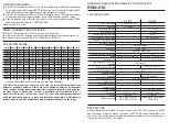
Figure 5-20. Synchronous Multiple (Burst) Read (GPMCFCLKDIVIDER = 1)
When GPMC_CONFIG5_i[20-16] RDACCESSTIME completes, control-signal timings are frozen during
the multiple data transactions, corresponding to GPMC_CONFIG5_i[27-24]
PAGEBURSTACCESSTIME multiplied by the number of remaining data transactions.
The CS, ADV, OE and DIR signals are controlled in the same way as for synchronous single read
operation. See
Initial latency for the first read data is controlled by RDACCESSTIME or by monitoring the WAIT signal.
Successive read data are provided by the memory device each one or two GPMC_CLK cycles. The
PAGEBURSTACCESSTIME parameter must be set accordingly with GPMC_CONFIG1_i[1-0]
GPMCFCLKDIVIDER and the memory-device internal configuration. Depending on the device page
length, the GPMC checks device page crossing during a new burst request and purposely insert initial
latency (of RDACCESSTIME) when required.
Total access time GPMC_CONFIG5_i[4-0] RDCYCLETIME corresponds to RDACCESSTIME plus the
address hold time from CS deassertion. In
, RDCYCLETIME programmed value equals to
RDCYCL RDCYCLETIME1.
After a read operation, if no other access (read or write) is pending, the data bus is driven with the
previous read value. See
Burst wraparound is enabled through the GPMC_CONFIG1_i[31] WRAPBURST bit and allows a 4-, 8-,
or 16-Word16 linear burst access to wrap within its burst-length boundary through
GPMC_CONFIG1_i[24-23] ATTACHEDDEVICEPAGELENGTH.
591
SPRUGX9 – 15 April 2011
General-Purpose Memory Controller (GPMC)
© 2011, Texas Instruments Incorporated


