BUS INTERFACE UNIT
3-18
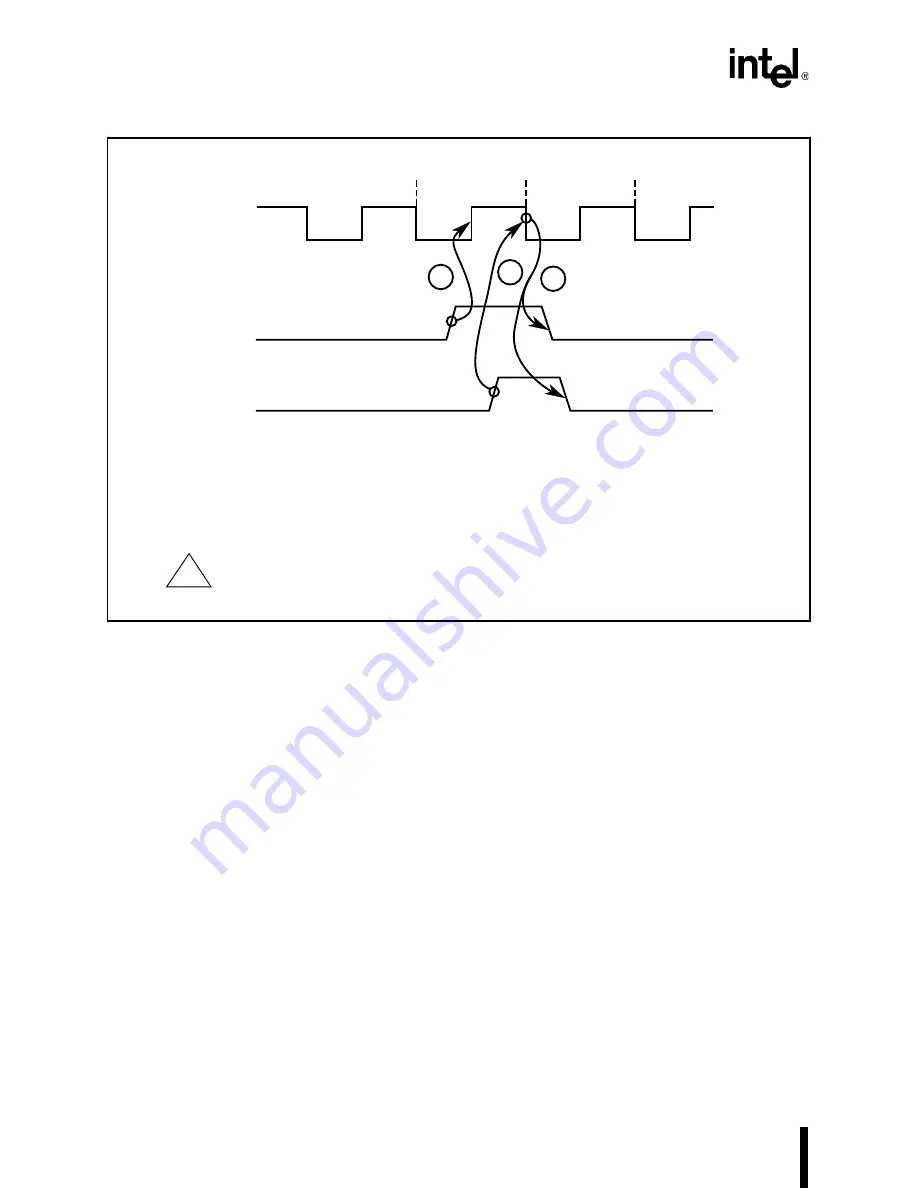
Figure 3-17. Normally Not-Ready System Timing
A valid not-ready input can be generated as late as phase 1 of T3 to insert wait states in a normally
ready system. A normally not-ready system must run wait states if the not-ready condition cannot
be met in time. Figure 3-18 illustrates the minimum and maximum timing necessary to insert wait
states in a normally ready system. Figure 3-18 also shows how to terminate a bus cycle with wait
states in a normally ready system.
The BIU can execute an indefinite number of wait states. However, bus cycles with large numbers
of wait states limit the performance of the CPU and the integrated peripherals. CPU performance
suffers because the instruction prefetch queue cannot be kept full. Integrated peripheral perfor-
mance suffers because the maximum bus bandwidth decreases.
3.4.4 Idle States
Under most operating conditions, the BIU executes consecutive (back-to-back) bus cycles. How-
ever, several conditions cause the BIU to become idle. An idle condition occurs between bus cy-
cles (see Figure 3-8 on page 3-9) and may last an indefinite period of time, depending on the
instruction sequence.
A1044-0A
ARDY
CLKOUT
T2
or T3
or TW
T4
In a Normally-Not-Ready system, wait states are inserted until (1 or 2) and 3 are met.
1. TCHIS
2. TCLIS
3. TCLIH
1
2
SRDY
3
: ARDY active to clock high (assumes ARDY remains active until 3).
: SRDY active to clock low.
: ARDY + SRDY hold from clock low.
!
Failure to meet SRDY setup and hold can cause a device failure
(i.e., the bus hangs or operates inappropriately).
T3
or TW
Summary of Contents for 80C186EA
Page 1: ...80C186EA 80C188EA Microprocessor User s Manual...
Page 2: ...80C186EA 80C188EA Microprocessor User s Manual 1995...
Page 19: ......
Page 20: ...1 Introduction...
Page 21: ......
Page 28: ...2 Overview of the 80C186 Family Architecture...
Page 29: ......
Page 79: ......
Page 80: ...3 Bus Interface Unit...
Page 81: ......
Page 129: ......
Page 130: ...4 Peripheral Control Block...
Page 131: ......
Page 139: ......
Page 140: ...5 ClockGenerationand Power Management...
Page 141: ......
Page 165: ......
Page 166: ...6 Chip Select Unit...
Page 167: ......
Page 190: ...7 Refresh Control Unit...
Page 191: ......
Page 205: ......
Page 206: ...8 Interrupt Control Unit...
Page 207: ......
Page 239: ...INTERRUPT CONTROL UNIT 8 32...
Page 240: ...9 Timer Counter Unit...
Page 241: ......
Page 265: ......
Page 266: ...10 Direct Memory Access Unit...
Page 267: ......
Page 295: ...DIRECT MEMORY ACCESS UNIT 10 28...
Page 296: ...11 Math Coprocessing...
Page 297: ......
Page 314: ...12 ONCE Mode...
Page 315: ......
Page 318: ...A 80C186 Instruction Set Additions and Extensions...
Page 319: ......
Page 330: ...B Input Synchronization...
Page 331: ......
Page 334: ...C Instruction Set Descriptions...
Page 335: ......
Page 383: ...INSTRUCTION SET DESCRIPTIONS C 48...
Page 384: ...D Instruction Set Opcodes and Clock Cycles...
Page 385: ......
Page 408: ...Index...
Page 409: ......


