OVERVIEW OF THE 80C186 FAMILY ARCHITECTURE
2-48
Single step priority is a special case. If an interrupt (NMI or maskable) occurs at the same instruc-
tion boundary as a single step, the interrupt vector is taken first, then is followed immediately by
the single step vector. However, the single step service routine is executed before the interrupt
service routine (see Figure 2-29). If the single step service routine re-enables single step by exe-
cuting the IRET, the interrupt service routine will also be single stepped. This can severely limit
the real-time response of the CPU to an interrupt.
To prevent the single-step routine from executing before a maskable interrupt, disable interrupts
while single stepping an instruction, then enable interrupts in the single step service routine. The
maskable interrupt is serviced from within the single step service routine and that interrupt ser-
vice routine is not single-stepped. To prevent single stepping before an NMI, the single-step ser-
vice routine must compare the return address on the stack to the NMI vector. If they are the same,
return to the NMI service routine immediately without executing the single step service routine.
Figure 2-29. Simultaneous NMI and Single Step Interrupts
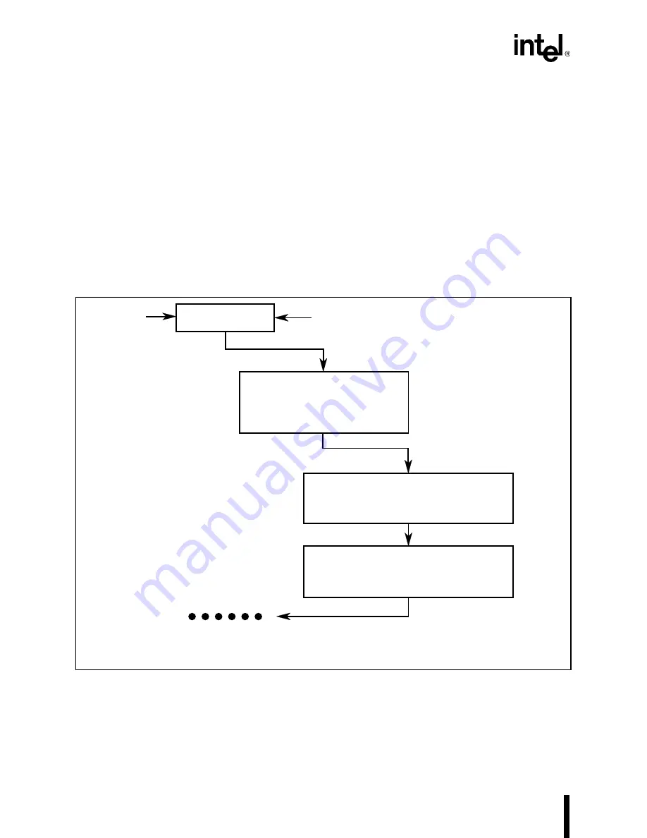
The most complicated case is when an NMI, a maskable interrupt, a single step and another ex-
ception are pending on the same instruction boundary. Figure 2-30 shows how this case is prior-
itized by the CPU. Note that if the single-step routine sets the Trap Flag (TF) bit before executing
the IRET instruction, the NMI routine will also be single stepped.
NMI
IRET
Instruction
Trap Flag = 1
Push PSW, CS, IP
Fetch Divide Error Vector
Trap Flag = 0
Execute Single Step
Service Routine
Push PSW, CS, IP
Fetch Single Step Vector
Trap Flag = ???
A1032-0A
Summary of Contents for 80C186EA
Page 1: ...80C186EA 80C188EA Microprocessor User s Manual...
Page 2: ...80C186EA 80C188EA Microprocessor User s Manual 1995...
Page 19: ......
Page 20: ...1 Introduction...
Page 21: ......
Page 28: ...2 Overview of the 80C186 Family Architecture...
Page 29: ......
Page 79: ......
Page 80: ...3 Bus Interface Unit...
Page 81: ......
Page 129: ......
Page 130: ...4 Peripheral Control Block...
Page 131: ......
Page 139: ......
Page 140: ...5 ClockGenerationand Power Management...
Page 141: ......
Page 165: ......
Page 166: ...6 Chip Select Unit...
Page 167: ......
Page 190: ...7 Refresh Control Unit...
Page 191: ......
Page 205: ......
Page 206: ...8 Interrupt Control Unit...
Page 207: ......
Page 239: ...INTERRUPT CONTROL UNIT 8 32...
Page 240: ...9 Timer Counter Unit...
Page 241: ......
Page 265: ......
Page 266: ...10 Direct Memory Access Unit...
Page 267: ......
Page 295: ...DIRECT MEMORY ACCESS UNIT 10 28...
Page 296: ...11 Math Coprocessing...
Page 297: ......
Page 314: ...12 ONCE Mode...
Page 315: ......
Page 318: ...A 80C186 Instruction Set Additions and Extensions...
Page 319: ......
Page 330: ...B Input Synchronization...
Page 331: ......
Page 334: ...C Instruction Set Descriptions...
Page 335: ......
Page 383: ...INSTRUCTION SET DESCRIPTIONS C 48...
Page 384: ...D Instruction Set Opcodes and Clock Cycles...
Page 385: ......
Page 408: ...Index...
Page 409: ......


