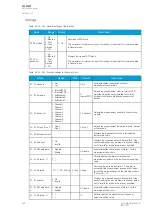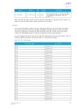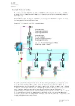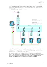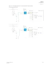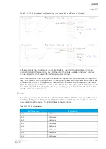
Figure. 5.4.32 - 176. Voltage angle drift.
The blocking signal for voltage memory can be found among other stage-related settings in the tab
VT
Module (3U/4U) 1. The blocking signal is checked in the beginning of each program cycle.
Measured input
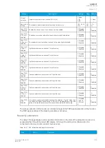
The function block uses analog voltage and current measurements' RMS values.
Table. 5.4.32 - 252. Measurement inputs of the voltage memory function.
Signal
Description
Time base
IL1RMS
RMS measurement of phase L1 (A) current
5ms
IL2RMS
RMS measurement of phase L2 (B) current
5ms
IL3RMS
RMS measurement of phase L3 (C) current
5ms
U
1
RMS
RMS measurement of voltage U
1
/V
5ms
U
2
RMS
RMS measurement of voltage U
2
/V
5ms
U
3
RMS
RMS measurement of voltage U
3
/V
5ms
U
4
RMS
RMS measurement of voltage U
4
/V
5ms
Voltage measurement modes 3LN and 3LL use three voltage inputs: channels U
A
, U
B
and U
C
. When
the voltage mode is set to 2LL, only two channels (U
A
and U
B
) are in use, and the memory is based on
the line-to-line voltages U
12
and U
32
. When the mode 2LL+U0 is used, the memory is based on
calculated phase-to-neutral voltages.
Pick-up
VMEM activ
VMEM activaation v
tion volta
oltage
ge and Mea
Measur
sured curr
ed current condition 3I>
ent condition 3I>
A
AQ
Q-M257
-M257
Instruction manual
Version: 2.07
338
© Arcteq Relays Ltd
IM00021
Содержание AQ-M257
Страница 1: ...AQ M257 Motor protection IED Instruction manual...
Страница 2: ......
Страница 449: ...Figure 7 3 221 Example block scheme A AQ Q M257 M257 Instruction manual Version 2 07 Arcteq Relays Ltd IM00021 447...
Страница 470: ...Figure 8 14 243 Device installation A AQ Q M257 M257 Instruction manual Version 2 07 468 Arcteq Relays Ltd IM00021...

