


User-Programmable Machines (UPMs)
MSC8113 Reference Manual, Rev. 0
Freescale Semiconductor
12-49
12.4.2 Programming the UPMs
The UPM is a microsequencer that requires microinstructions or RAM words to generate signal
timings for different memory cycles. Follow these steps to program the UPMs:
1.
Set up BRx and ORx.
2.
Write patterns into the RAM array.
3.
Program MPTPR and PURT if refresh is required.
4.
Program the Machine Mode Register (MxMR).
To write patterns to the RAM array, set MxMR[OP] = 01 and access the UPM with a single byte
transaction.
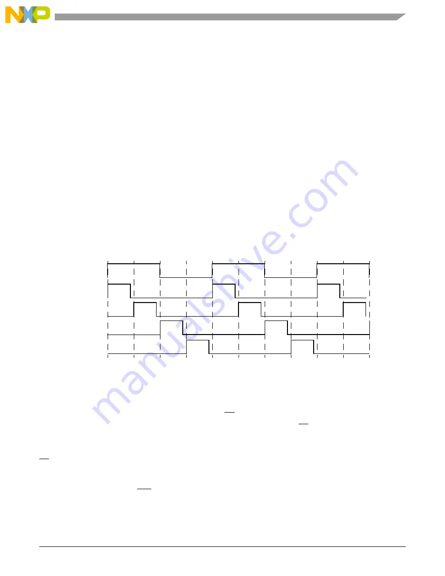
12.4.3 Clock Timing
Fields in the RAM word specify the value of various external signals at each clock edge. The
signal timing generator causes external signals to behave according to the timing specified in the
current RAM word. Figure 12-49 shows the clock schemes of the UPMs in the memory
controller. Note that the width of T1/2/3/4 are equal. The clock phases shown reflect timing
windows during which generated signals can change state.
The state of the external signals may change (if specified in the RAM array) at any positive edge
of
T1
,
T2
,
T3
, or
T4
(there is a propagation delay specified in Section 2, Hardware Specifications,
of the MSC8113 Data sheet). However, only the
CS
signal corresponding to the currently
accessed bank is manipulated by the UPM pattern when it runs. The
BS
signal assertion and
deassertion timing is also specified for each cycle in the RAM word. The port size of the
specified bank, the external address accessed, and the value of
TSZ
determine which of the eight
BS
signals are manipulated. The
PGPL
lines toggle as programmed for any access that initiates a
particular pattern, but control resolution is limited to
T1
and
T3
.
CSx
,
PGPL1
, and
PGPL2
are controlled. A word is read from the RAM
which specifies the logical bits CST1, CST2, CST3, CST4, G1T1, G1T3, G2T1, and G2T3.
These bits determine the corresponding output signal level for each clock.
Figure 12-49. UPM Clock Scheme
Bus CLK
T1
T2
T3
T4
Summary of Contents for MSC8113
Page 1: ...MSC8113 Reference Manual Tri Core 16 Bit Digital Signal Processor MSC8113RM Rev 0 May 2008 ...
Page 20: ...MSC8113 Reference Manual Rev 0 xx Freescale Semiconductor Contents ...
Page 28: ...MSC8113 Reference Manual Rev 0 xxviii Freescale Semiconductor ...
Page 56: ...MSC8113 Reference Manual Rev 0 1 28 Freescale Semiconductor MSC8113 Overview ...
Page 76: ...MSC8113 Reference Manual Rev 0 2 20 Freescale Semiconductor SC140 Core Overview ...
Page 134: ...MSC8113 Reference Manual Rev 0 4 30 Freescale Semiconductor System Interface Unit SIU ...
Page 168: ...MSC8113 Reference Manual Rev 0 6 18 Freescale Semiconductor Boot Program ...
Page 180: ...MSC8113 Reference Manual Rev 0 7 12 Freescale Semiconductor Clocks ...
Page 260: ...MSC8113 Reference Manual Rev 0 8 80 Freescale Semiconductor Memory Map ...
Page 300: ...MSC8113 Reference Manual Rev 0 9 40 Freescale Semiconductor Extended Core ...
Page 304: ...MSC8113 Reference Manual Rev 0 10 4 Freescale Semiconductor MQBus and M2 Memory ...
Page 308: ...MSC8113 Reference Manual Rev 0 11 4 Freescale Semiconductor SQBus ...
Page 590: ...MSC8113 Reference Manual Rev 0 17 46 Freescale Semiconductor Interrupt Processing ...
Page 614: ...MSC8113 Reference Manual Rev 0 18 24 Freescale Semiconductor Debugging ...
Page 622: ...MSC8113 Reference Manual Rev 0 19 8 Freescale Semiconductor Internal Peripheral Bus IPBus ...
Page 724: ...MSC8113 Reference Manual Rev 0 21 32 Freescale Semiconductor UART ...
Page 920: ...MSC8113 Reference Manual Rev 0 25 150 Freescale Semiconductor Ethernet Controller ...
Page 1171: ...MSC8113 Reference Manual Rev 0 Freescale Semiconductor C 61 EF wait_rts P 01077FFC 9F rts 71 ...
Page 1172: ...MSC8113 Reference Manual Rev 0 C 62 Freescale Semiconductor MSC8113 Boot Code ...
Page 1202: ...MSC8113 Reference Manual Rev 0 Index 30 Freescale Semiconductor Index ...


