-
121
-
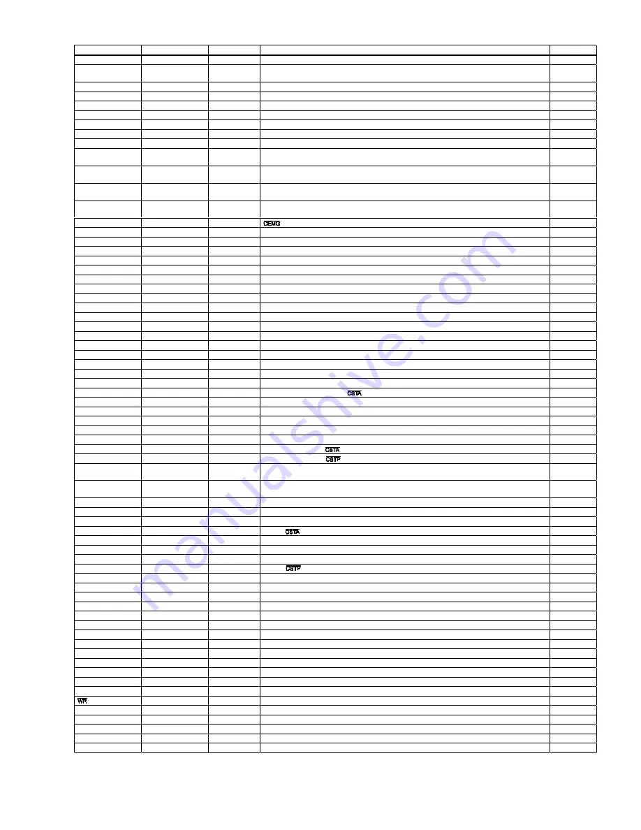
Label
Type
Position
Description
Reference
SDLT
Register
bit
RENV1
5
Specify
the
latch
function
for
the
SD
input
(0:
ON,
1:
OFF)
P38
SDM
Register
bit
RENV1
4
Select
the
process
to
execute
when
the
SD
input
is
ON
(0:
Deceleration
only,
1:
Decelerate
and
stop)
P38
SDRM
Register
bit
RSTS
12
Equals
1
when
the
-DR
(PB)
input
signal
is
ON
P45
SDRP
Register
bit
RSTS
11
Equals
1
when
the
+DR
(PA)
input
signal
is
ON
P45
SDSTP
Command
4Ah
Deceleration
stop
P25
SDu
Terminal
name
132 Ramping-down
signal
for
the
U
axis
(PCL6143)
P10
SDx
Terminal
name
38,
39 Ramping-down
signal
for
the
X
axis
(PCL6123,
6143)
P10
SDy
Terminal
name
75,
70 Ramping-down
signal
for
the
Y
axis
(PCL6123,
6143)
P10
SDz
Terminal
name
101 Ramping-down
signal
for
the
Z
axis
(PCL6143)
P10
SELu
Command
bit
name
COMW
11
Select
the
U
axis
P20
SELx
Command
bit
name
COMW
8
Select
the
X
axis
P20
SELy
Command
bit
name
COMW
9
Select
the
Y
axis
P20
SELz
Command
bit
name
COMW
10
Select
the
Z
axis
P20
SEMG
Register
bit
RSTS
7
Input
signal
is
ON
P45
SEND
Main
status
bit
MSTSW
3
Equals
0
when
started
automatically,
becomes
1
when
stopped
P22
SENI
Main
status
bit
MSTSW
2
Equals
1
when
an
interrupt
is
caused
by
stopping.
P22
SEOR
Main
status
bit
MSTSW
13
Equals
1
when
unable
to
execute
a
position
override.
P22
SERC
Register
bit
RSTS
9
Equals
1
when
the
ERC
output
signal
is
ON
P45
SERR
Main
status
bit
MSTSW
4
Equals
1
when
an
error
interrupt
occurs
P22
SEZ
Register
bit
RSTS
10
Equals
1
when
the
EZ
input
signal
is
ON
P45
SFC
Sub-status
bit
SSTSW
10
Equals
1
when
feeding
at
low
speed
P23
SFD
Sub-status
bit
SSTSW
9
Equals
1
when
decelerating
P23
SFU
Sub-status
bit
SSTSW
8
Equals
1
when
accelerating
P23
SINP
Register
bit
RSTS
15
Equals
1
when
the
INP
input
signal
is
ON
P45
SINT
Main
status
bit
MSTSW
5
Equals
1
when
an
event
interrupt
occurs
P22
SLTC
Register
bit
RSTS
13
Equals
1
when
the
LTC
input
signal
is
ON
P45
SMEL
Sub-status
bit
SSTSW
13
Equals
1
when
the
-EL
input
is
ON
P23
SORG
Sub-status
bit
SSTSW
14
Equals
1
when
the
ORG
input
is
ON
P23
SPCS
Register
bit
RSTS
8
Equals
1
when
the
PCS
input
signal
is
ON
P45
SPEL
Sub-status
bit
SSTSW
12
Equals
1
when
the
+EL
input
is
ON
P23
SPRF
Main
status
bit
MSTSW
14
Equals
1
when
the
next-operation
pre-register
is
full
P22
SPSTA
Command
2Ah
The
same
process
as
the
input
P25
SRST
Command
04h
Software
reset
P27
SRUN
Main
status
bit
MSTSW
1
Equals
1
while
starting
P22
SSC0
to
1
Main
status
bits
MSTSW
6-7
Sequence
code
P22
SSCM
Main
status
bit
MSTSW
0
Equals
1
when
a
start
command
has
already
been
written
P22
SSD
Sub-status
bit
SSTSW
15
Equals
1
when
the
SD
input
is
ON
(latched
signal)
P23
SSTA
Register
bit
RSTS
5
Equals
1
when
the
input
signal
is
ON
P45
SSTP
Register
bit
RSTS
6
Equals
1
when
the
input
signal
is
ON
P45
SSTSB
Byte
map
name
3
when
using
a
Z80
Used
to
read
the
sub
status
P23
SSTSW
Word
map
name
2
when
using
an
8086
Used
to
read
the
sub
status,
general
input/output
port
P18
STAD
Command
52h
High
speed
start
1
(FH
low
speed
->
deceleration
stop)
P24
STAFH
Command
51h
Start
using
FH
low
speed
P24
STAFL
Command
50h
Start
using
FL
low
speed
P24
STAM
Register
bit
RENV1
18
Select
signal
input
specification
(0:
Level
trigger,
1:
Edge
trigger)
P39
STAON
Command
28h
Substitute
for
a
PCs
input
P27
STAUD
Command
53h
High
speed
start
2
(acceleration
->
FH
low
speed
->
deceleration
stop)
P24
STOP
Command
49h
Immediate
stop
P24
STPM
Register
bit
RENV1
19
Select
stop
method
(0:
Immediate
stop,
1:
Deceleration
stop)
P39
SYI0
to
1
Register
bits
RENV3
20-21 Select
the
axis
used
to
input
an
internal
synchronous
signal
P42,
96
SYO0
to
3
Register
bits
RENV3
16-19 Set
the
output
timing
of
the
internal
synchronous
signal
P42,
96
WPRDP
Command
86h
Write
BUF
data
into
PRDP
P29
WPRDR
Command
84h
Write
BUF
data
into
PRDR
P29
WPRDS
Command
8Ah
Write
BUF
data
into
PRDS
P29
WPRFH
Command
82h
Write
BUF
data
into
PRFH
P29
WPRFL
Command
81h
Write
BUF
data
into
PRFL
P29
WPRIP
Command
88h
Write
BUF
data
into
PRIP
P29
WPRMD
Command
87h
Write
BUF
data
into
PRMD
P29
WPRMG
Command
85h
Write
BUF
data
into
PRMG
P29
WPRMV
Command
80h
Write
BUF
data
into
PRMV
P29
WPRUR
Command
83h
Write
BUF
data
into
PRUR
P29
WPRUS
Command
89h
Write
BUF
data
into
PRUS
P29
Terminal
name
6,
6,
6 Write
signal
(PCL6113,
6123,
6143)
P8
WRCMP1
Command
A7h
Write
BUF
data
into
the
RCMP1
register
P29
WRCMP2
Command
A8h
Write
BUF
data
into
the
RCMP2
register
P29
WRCUN1
Command
A3h
Write
BUF
data
into
the
RCUN1
register
P29
WRCUN2
Command
A4h
Write
BUF
data
into
the
RCUN2
register
P29
WRDP
Command
96h
Write
BUF
data
into
the
RDP
register
P29
Summary of Contents for PCL6113
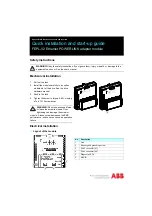
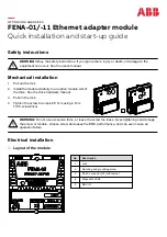
Page 1: ...User s Manual For PCL6113 6123 6143 Pulse Control LSI Nippon Pulse Motor Co Ltd...
Page 11: ...5 3 Terminal Assignment Diagram 3 1 PCL6113 3 2 PCL6123...
Page 20: ...14 5 Block Diagram...
Page 115: ...109 11 Stop timing by error...
Page 116: ...110 13 External Dimensions 13 1 PCL6113...
Page 117: ...111 13 2 PCL6123...
Page 118: ...112 13 3 PCL6143...


