MAX32600 User’s Guide
Analog Front End
8.4 DAC
DAC Power-Up and Enable Sequence
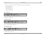
Once the DAC module clock has been enabled, the DAC instance itself may be powered on and enabled for use by the application firmware. In order to do this, the
following register settings must be made in the
register.
Note
These writes do not have to be made one at a time; all the fields listed below can be written in a single write to
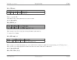
• Write
to 1. This will cause the DAC timing generator and other internal logic to be reset (but will not reset the contents of the DAC
registers). This bit is self-clearing and will automatically clear back to 0 after the DAC is reset.
• Write
to 1. This will turn on the clock for the DAC logic.
• Write
to 1. This powers up the DAC analog circuitry.
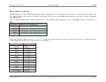
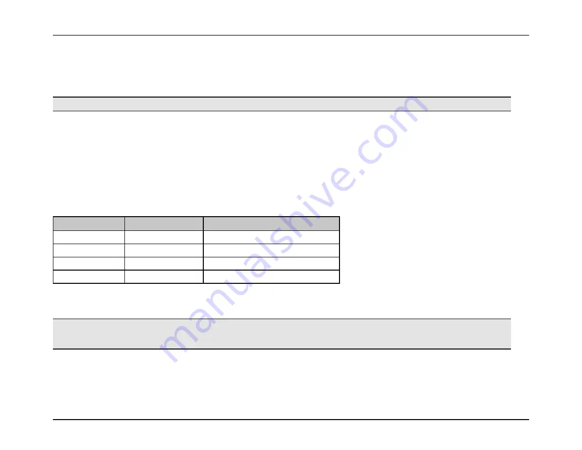
• When powering up one of the 12-bit DAC instances (DAC0 or DAC1), the DAC power mode must be selected; this mode is specified by the combination of the
and
fields as shown
. If any power level other than FullPwr is used, then the negative
DAC output should be used and other compensations made as described in the
Reduced Power Level Modes for 12-bit DAC Instances
section.
power_mode_2 (1b)
power_mode_1_0 (2b)
DAC Power Level (DAC0 and DAC1 only)
0
01b
PwrLvl0 (48uA)
0
11b
PwrLvl1 (130uA)
1
01b
PwrLvl2 (210uA)
1
11b
FullPwr Mode (291uA)
Selecting the DAC Sample Rate and Interpolation Mode
Note
The settings described below only apply if the DAC will be used to generate a dynamic output voltage pattern by loading a series of sample code
values into the DAC FIFO. If the DAC will be used to generate a static output voltage by loading a single value into the DAC FIFO, then these settings
do not need to be written.
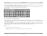
Along with the DAC module clock, there are two additional parameters which determine the rate at which the voltage value changes at the DAC output.
• The
Rate Count parameter
determines the delay (measured in number of DAC clock cycles) between one output voltage from the DAC and the next.
Rev.1.3 April 2015
Maxim Integrated
Page 456

