MAX32600 User’s Guide
System Clock, Timers/Counters, Watchdog Timers and Real Time Clock
10.1 System Clock
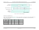
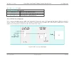
Figure 10.3: Phase Lock Loop Functional Diagram
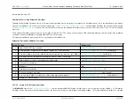
Firmware Control of the Phase Lock Loop
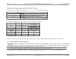
The PLL is disabled by default. However, the PLL is needed to generate the required 48MHz clock for USB operation. The PLL can multiply an 8MHz, 12MHz, or
24MHz clock up to the required 48MHz. The
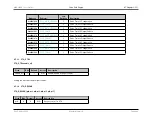
register settings for the most common applications are detailed in the table below.
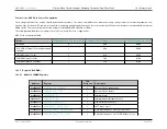
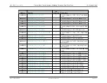
PLL Firmware Configuration Table
Mode
Disabled
0
0
0
00b
Relax Oscillator Input
1
1
1
00b
8Mhz Crystal Input
1
1
0
1xb
12Mhz Crystal Input
1
1
0
01b
24Mhz Crystal Input
1
1
0
00b
Rev.1.3 April 2015
Maxim Integrated
Page 506


