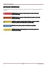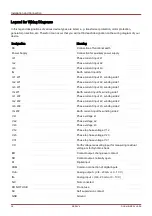
IMPORTANT DEFINITIONS
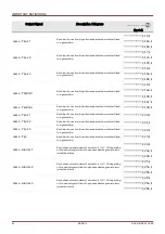
Output Signal
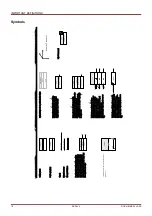
Description / Diagram
────────────────
➁
(Symbol)
name . Alarm
Each phase selective alarm of a module (I, IG, V, VX depending
on the device type) will lead to a phase selective general alarm
(collective alarm).
─────────
❨27❩
─────────
❨27a❩
─────────
❨27b❩
─────────
❨27c❩
─────────
❨27d❩
name . Alarm L1
Each phase selective alarm of a module (I, IG, V, VX depending
on the device type) will lead to a phase selective general alarm
(collective alarm).
─────────
❨28❩
name . Alarm L2
Each phase selective alarm of a module (I, IG, V, VX depending
on the device type) will lead to a phase selective general alarm
(collective alarm).
─────────
❨29❩
name . Alarm L3
Each phase selective alarm of a module (I, IG, V, VX depending
on the device type) will lead to a phase selective general alarm
(collective alarm).
─────────
❨30❩
name . Alarm
Each phase selective alarm of a module (I, IG, V, VX depending
on the device type) will lead to a phase selective general alarm
(collective alarm).
─────────
❨31❩
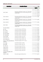
Prot . Blo TripCmd
─────────
❨32❩
CB . Pos
Please Refer To Diagram: CB.CB Manager
─────────
❨33❩
CB . Pos ON
Please Refer To Diagram: CB.CB Manager
─────────
❨34❩
CB . Pos OFF
Please Refer To Diagram: CB.CB Manager
─────────
❨35❩
CB . Pos Indeterm
Please Refer To Diagram: CB.CB Manager
─────────
❨36❩
CB . Pos Disturb
Please Refer To Diagram: CB.CB Manager
─────────
❨37❩
LOP . LOP Blo
Please Refer To Diagram: LOP.LOP Blo
─────────
❨38a❩
LOP . Ex FF VT-I
Please Refer To Diagram: LOP.Ex FF VT
─────────
❨38b❩
LOP . Ex FF EVT-I
Please Refer To Diagram: LOP.Ex FF EVT
─────────
❨38c❩
Q->&V< . Decoupling Distributed
Generator
Please Refer To Diagram: Q->&V<: “QU_Y02”
─────────
❨39❩
CTS . Alarm
Please Refer To Diagram: CTS.Alarm
─────────
❨40❩
SG.Prot ON
Please Refer To Diagram: SG.Prot ON
─────────
❨41❩
SG . ON Cmd
Please Refer To Diagram: SG.ON Cmd
─────────
❨42❩
AnIn[1] . Value
Please Refer To Diagram: Analog values
─────────
❨43❩
AnIn[2] . Value
Please Refer To Diagram: Analog values
─────────
❨44❩
AnIn[n] . Value
Please Refer To Diagram: Analog values
─────────
❨45❩
Trip Incomplete (Motor) Start
Sequence
─────────
❨46❩
Q->&V< . active
Please refer to diagram: Blocking (Q->&V<)
─────────
❨47❩
24
MCDLV4
DOK-HB-MCDLV4-2E
Содержание HighPROtec MCDLV4
Страница 1: ...Manual Line Differential Protection MCDLV4 Software Version 3 4 a DOK HB MCDLV4 2E Revision A English...
Страница 3: ...Order Code Order Code 3 MCDLV4 DOK HB MCDLV4 2E...
Страница 47: ...Installation and Connection 47 MCDLV4 DOK HB MCDLV4 2E...
Страница 164: ...Input Output and LED Settings 164 MCDLV4 DOK HB MCDLV4 2E...
Страница 433: ...Parameters 433 MCDLV4 DOK HB MCDLV4 2E...
Страница 457: ...Device Parameters 457 MCDLV4 DOK HB MCDLV4 2E...
Страница 473: ...Blockings 473 MCDLV4 DOK HB MCDLV4 2E...
Страница 822: ...Protective Elements Name Description Profibus Scada Cmd 16 Scada Command 822 MCDLV4 DOK HB MCDLV4 2E...
Страница 988: ...Protective Elements 988 MCDLV4 DOK HB MCDLV4 2E P P Q P Q P Q Q Q P S S...
Страница 989: ...Protective Elements 989 MCDLV4 DOK HB MCDLV4 2E Pr Q P Q P Qr...
Страница 1023: ...Protective Elements 1023 MCDLV4 DOK HB MCDLV4 2E...
Страница 1070: ...Supervision 1070 MCDLV4 DOK HB MCDLV4 2E...

