background image

General Lists

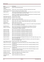
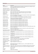
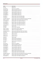
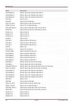
Name

Description

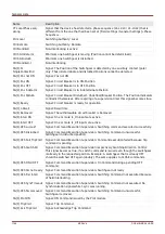
SG[1].WearLevel Alarm

Signal: Threshold for the Alarm

SG[1].WearLevel 

Lockout

Signal: Threshold for the Lockout Level

SG[1].Res CB OPEN 
capacity

Signal: Reset of the wear maintenance curve (i. e. of the counter for the Circuit 
Breaker OPEN capacity.

SG[1].Isum Intr ph Alm

Signal: Alarm, the per hour Sum (Limit) of interrupting currents has been exceeded.

SG[1].Res Isum Intr ph 

Alm

Signal: Reset of the Alarm, "the per hour Sum (Limit) of interrupting currents has 

been exceeded".

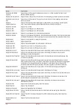
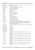
SG[2].SI 
SingleContactInd

Signal: The Position of the Switchgear is detected by one auxiliary contact (pole) 
only. Thus indeterminate and disturbed Positions cannot be detected.

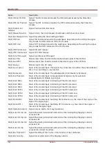
SG[2].Pos not ON

Signal: Pos not ON

SG[2].Pos ON

Signal: Circuit Breaker is in ON-Position

SG[2].Pos OFF

Signal: Circuit Breaker is in OFF-Position

SG[2].Pos Indeterm

Signal: Circuit Breaker is in Indeterminate Position

SG[2].Pos Disturb

Signal: Circuit Breaker Disturbed - Undefined Breaker Position. The Position Indicators 

contradict themselves. After expiring of a supervision timer this signal becomes true.

SG[2].Ready

Signal: Circuit breaker is ready for operation.

SG[2].t-Dwell

Signal: Dwell time

SG[2].Removed

Signal: The withdrawable circuit breaker is Removed

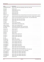
SG[2].Interl ON

Signal: One or more IL_On inputs are active.

SG[2].Interl OFF

Signal: One or more IL_Off inputs are active.

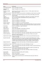
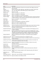
SG[2].CES succesf

Signal: Command Execution Supervision: Switching command executed successfully.

SG[2].CES Disturbed

Signal: Command Execution Supervision: Switching Command unsuccessful. 
Switchgear in disturbed position.

SG[2].CES Fail TripCmd

Signal: Command Execution Supervision: Command execution failed because trip 

command is pending.

SG[2].CES SwitchDir

Signal: Command Execution Supervision respectively Switching Direction Control: 
This signal becomes true, if a switch command is issued even though the switchgear 

is already in the requested position. Example: A switchgear that is already OFF 
should be switched OFF again (doubly). The same applies to CLOSE commands.

SG[2].CES ON d OFF

Signal: Command Execution Supervision: On Command during a pending OFF 

Command.

SG[2].CES SG not ready Signal: Command Execution Supervision: Switchgear not ready
SG[2].CES Fiel Interl

Signal: Command Execution Supervision: Switching Command not executed because 
of field interlocking.

SG[2].CES SyncTimeout Signal: Command Execution Supervision: Switching Command not executed. No 

Synchronization signal while t-sync was running.

SG[2].CES SG removed

Signal: Command Execution Supervision: Switching Command unsuccessful, 
Switchgear removed.

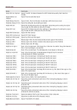
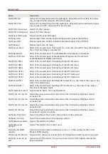
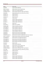
SG[2].Prot ON

Signal: ON Command issued by the Prot module

SG[2].TripCmd

Signal: Trip Command

SG[2].Ack TripCmd

Signal: Acknowledge Trip Command

SG[2].ON incl Prot ON

Signal: The ON Command includes the ON Command issued by the Protection 

module.

1160

MCDLV4

DOK-HB-MCDLV4-2E

Содержание HighPROtec MCDLV4

Страница 1: ...Manual Line Differential Protection MCDLV4 Software Version 3 4 a DOK HB MCDLV4 2E Revision A English...

Страница 2: ...urrent and Volt unbalance THD and THD Fund and RMS Max Min Avg phasors and angles Power Fund and RMS P Q S PF Metering Statistics and Demand Inrush 79 CTS 47 Standard 55 LOP 32 25 1 0 59N 59A 27A Prog...

Страница 3: ...Order Code Order Code 3 MCDLV4 DOK HB MCDLV4 2E...

Страница 4: ...0 RTU RS485 terminals B Modbus TCP DNP3 0 TCP UDP Ethernet 100 MB RJ45 C Profibus DP optic fiber ST connector D Profibus DP RS485 D SUB E Modbus RTU IEC60870 5 103 DNP3 0 RTU optic fiber ST connector...

Страница 5: ...gic up to 80 equations The type of cards are as follows for the three main variants Variant Slot X1 Slot X2 Slot X3 Slot X4 Slot X5 Slot X6 MCDLV4 2 A DI8 X1 RO 6 X2 TI 4 TIS 4 cur transf TU volt tran...

Страница 6: ...Slot X1 Power Supply Card with Digital Inputs 38 Slot X2 Relay Output Card 42 Slot X3 Current Transformer Measuring Inputs 45 Slot X4 Voltage Transformer Measuring Inputs 56 Slot X5 Multi Input Outpu...

Страница 7: ...of the Demand Management 245 Signals of the Demand Management States of the Outputs 245 Global Protection Parameter of the Demand Management 246 States of the Inputs of the Demand Management 250 Ackno...

Страница 8: ...Prot 479 Blocking all Protective Elements enduringly 479 Blocking all Protective Elements temporarily 479 Blocking all Trip Commands enduringly 480 Blocking all Trip Commands temporarily 480 General...

Страница 9: ...Shedding 942 LVRT Low Voltage Ride Through 27 t 961 Intertripping Remote 977 PQS Power 32 37 985 PF Power Factor 55 1005 ExP External Protection 1014 Ext Temp Superv Protection Module External Tempera...

Страница 10: ...with LC Connector for Long distance Protection Communication 1146 Boot phase 1148 Servicing and Maintenance 1149 Standards 1150 Approvals 1150 Design Standards 1150 High Voltage Tests 1151 EMC Immunit...

Страница 11: ...Table of Contents md5_1 md5_2 RMS Handoff 0 File generated DOK HB MCDLV4 2E_A pdf This manual applies to devices version Version 3 4 a Build 35594 11 MCDLV4 DOK HB MCDLV4 2E...

Страница 12: ...descriptions this manual includes Text graphic and formulae do not always apply to the actual delivery scope The drawings and graphics are not true to scale We do not accept any liability for damage a...

Страница 13: ...th or serious injury WARNING indicates a hazardous situation which if not avoided could result in death or serious injury CAUTION used with the safety alert symbol indicates a hazardous situation whic...

Страница 14: ...hat is to be protected You must ensure that the device will properly recognize and manage e g switch off the circuit breaker on the basis of your programming and parameterization all operational condi...

Страница 15: ...ion of our website www woodward com If your publication is not there please contact your customer service representative to get the latest copy Important Information In line with the customer s requir...

Страница 16: ...e work area as much as possible 4 Do not remove any printed circuit board PCB from the control cabinet unless absolutely necessary If you must remove the PCB from the control cabinet follow these prec...

Страница 17: ...entation as well as the parameter setting and evaluation software Please check the consignment for completeness on arrival delivery note Please ascertain whether the type plate connection diagram type...

Страница 18: ...pecially reserved for this purpose In general appropriate local guidelines and regulations must be followed when disposing of electrical devices and batteries Purpose of the Battery The purpose of the...

Страница 19: ...a pre defined value can be selected 1 n Assignment List name 1 n VeEnable no assignment 1 n no assignm ent 1 name 1 n Assignment List Parameter of a Module Input with special values An 1 n output from...

Страница 20: ...ll be reset by 0 at the input Thus the output will be set to 0 at the same time Time stage minimum pulse width The pulse width name t will be started if a 1 is feed to the input By starting name t the...

Страница 21: ...talic SIGNALS are indicated by right and left double arrow heads and small caps Paths are indicated by brackets Software and Device names are written in italic Module and Instance Element names are di...

Страница 22: ...e protective device Please Refer To Diagram Blockings only for line differential protection 4R IH2 Blo L1 Please Refer To Diagram IH2 5 IH2 Blo L2 Please Refer To Diagram IH2 6 IH2 Blo L3 Please Refer...

Страница 23: ...ion module will lead to a general trip 20 name Trip L2 Each trip of an active trip authorized protection module will lead to a general trip 21 name Trip L3 Each trip of an active trip authorized prote...

Страница 24: ...to a phase selective general alarm collective alarm 31 Prot Blo TripCmd 32 CB Pos Please Refer To Diagram CB CB Manager 33 CB Pos ON Please Refer To Diagram CB CB Manager 34 CB Pos OFF Please Refer To...

Страница 25: ...n only be read within this level This level enables execution of Resets and Acknowledgements This level enables modification of protection settings This level provides full access not limited to all s...

Страница 26: ...TIONS Load Reference Arrow System Within the HighPROTEC the Load Reference Arrow System is used in principal Generator protection relays are working based on the Generator Reference System 26 MCDLV4 D...

Страница 27: ...taken into account that by deactivating for instance protective functions you also change the functionality of the device If you cancel the directional feature of the overcurrent protections then the...

Страница 28: ...output relays MCDLV4 Hardware Variant 2 Optional Hardware Extension 0 Phase Current 5A 1A Ground Current 5A 1A 1 Phase Current 5A 1A Sensitive Ground Current 5A 1A Phase Current 5A 1A Ground Current 5...

Страница 29: ...870 5 103 DNP RTU H Ethernet IEC61850 Modbus TCP DNP UDP TCP I RS 485 Ethernet Modbus TCP RTU IEC 60870 5 103 DNP UDP TCP RTU K Ethernet Fiber Optics IEC61850 Modbus TCP DNP UDP TCP L Ethernet Fiber O...

Страница 30: ...DA system used the needed space depth differs If for instance a D Sub Plug is used it has to be added to the depth dimension The three side view shown in this section is exclusively valid for 19 devic...

Страница 31: ...vice Moreover the power supply card needs a separate ground connection functional earth min 2 5 mm2 AWG 13 tightening torque 0 56 0 79 Nm 5 7 lb in See the Terminal Marking diagram in Section DI 4 X P...

Страница 32: ...xcept dimensions in brackets inch The housing must be carefully grounded Connect a ground cable protective earth 4 to 6 mm2 AWG 11 9 tightening torque 1 7 Nm 15 lb in to the housing using the screw th...

Страница 33: ...15 lb in to the housing using the screw that is marked with the ground symbol at the rear side of the device Moreover the power supply card needs a separate ground connection functional earth min 2 5...

Страница 34: ...ly group may be integrated In the following the terminal assignment of the individual assembly groups are shown The exact installation place of the individual modules can be learned from the connectio...

Страница 35: ...upply card needs a separate ground connection functional earth min 2 5 mm2 AWG 13 tightening torque 0 56 0 79 Nm 5 7 lb in See the Terminal Marking diagram in Section DI 4 X Power Supply and Digital I...

Страница 36: ...nt input L3 winding side 1 I G W1 Earth current input IG winding side 1 I L1 W2 Phase current input L1 winding side 2 I L2 W2 Phase current input L2 winding side 2 I L3 W2 Phase current input L3 windi...

Страница 37: ...xternal galvanic decoupled CTs See chapter Current Transformers of the manual Only for use with external galvanic decoupled CTs See chapter Current Transformers of the manual Caution Sensitive Current...

Страница 38: ...device type The different variants have a different scope of functions Available assembly groups in this slot DI8 X1 This assembly group comprises a wide range power supply unit and two non grouped d...

Страница 39: ...Installation and Connection DI8 X Power Supply and Digital Inputs Ensure the correct tightening torques 39 MCDLV4 DOK HB MCDLV4 2E 0 56 0 79 Nm 5 7 lb in 0 3 Nm 2 65 lb in...

Страница 40: ...power supply unit are non polarized The device could be provided with AC or DC voltage Digital inputs For each digital input group the related voltage input range has to be parameterized Wrong switchi...

Страница 41: ...8 9 10 11 12 COM1 13 14 15 16 17 18 L Power Supply DI1 COM2 DI2 COM3 DI3 DI4 DI5 DI6 DI7 DI8 COM do not use do not use L X n c Functional Earth L L COM1 DI1 COM2 DI2 DI3 DI4 DI5 DI6 DI7 DI8 COM3 dono...

Страница 42: ...ordered device type The different variants have a different scope of functions Available assembly groups in this slot RO 6 X2 Assembly Group with 6 Relay Outputs The available combinations can be gath...

Страница 43: ...ts In chapter Assignment binary outputs the assignment of the binary output relays is specified The changeable signals are listed in the assignment list which can be found in the appendix Ensure the c...

Страница 44: ...V4 DOK HB MCDLV4 2E 1 2 3 4 5 6 7 8 9 10 11 12 13 14 15 16 17 18 BO3 BO1 BO2 BO4 BO5 BO6 X BO1 C BO1 n o BO1 n c BO2 C BO2 n o BO2 n c BO3 C BO3 n o BO3 n c BO4 C BO4 n o BO4 n c BO5 C BO5 n o BO5 n c...

Страница 45: ...ive ground current measuring card Available assembly groups in this slot TI 4 X3 Standard ground current measuring card TIS 4 X3 Sensitive Ground current measuring card The Technical data of the sensi...

Страница 46: ...t circuited before the current circuit to the device is opened The current measuring inputs may exclusively be connected to current measuring transformers with galvanic separation Do not interchange t...

Страница 47: ...Installation and Connection 47 MCDLV4 DOK HB MCDLV4 2E...

Страница 48: ...Electro mechanical assignment 48 MCDLV4 DOK HB MCDLV4 2E 1 2 3 4 5 6 7 8 9 10 11 12 IL1 1A 5A N IL2 1A 5A N IL3 1A 5A N IG 1A 5A N X IL1 1A IL1 N IL1 5A IL2 1A IL2 N IL3 1A IL3 N IL3 5A IG 1A IG N IG...

Страница 49: ...ry insulation functionality All current measuring inputs can be provided with 1 A or 5 A nominal Make sure that the wiring is correct Sensitive Ground Current Measurement The proper use of sensitive c...

Страница 50: ...ansformer Connection Examples 50 MCDLV4 DOK HB MCDLV4 2E L1 L2 L3 IL1 IL2 IL3 1 X 2 3 4 5 6 7 8 9 10 11 12 Three phase current measurement In secondary 5 A IL1 1A 5A N IL2 1A 5A N IL3 1A 5A N IG 1A 5A...

Страница 51: ...1A 5A N IL2 1A 5A N IL3 1A 5A N IG 1A 5A N Warning The shielding at the dismantled end of the line has to be put through the cable type current transformer and has to be grounded at the cable side Rin...

Страница 52: ...LV4 2E L1 L2 L3 IL2 IL1 IL3 IL2 IL3 IL1 1 X 2 3 4 5 6 7 8 9 10 11 12 IG Three phase current measurement In secondary 5 A Earth current measuring via Holmgreen connection IGnom secondary 5 A IL1 1A 5A...

Страница 53: ...LV4 2E L1 L2 L3 IL1 IL2 IL3 1 X 2 3 4 5 6 7 8 9 10 11 12 IG Three phase current measurement In secondary 1 A Earth current measuring via Holmgreen connection IGnom secondary 1 A IL1 1A 5A N IL2 1A 5A...

Страница 54: ...IG IL1 1A 5A N IL2 1A 5A N IL3 1A 5A N IG 1A 5A N Warning The shielding at the dismantled end of the line has to be put through the cable type current transformer and has to be grounded at the cable...

Страница 55: ...LV4 2E L1 L3 L2 IL1 IL3 IL2 1 X 2 3 4 5 6 7 8 9 10 11 12 IG Three phase current measurement In secondary 1 A Earth current measuring via Holmgreen connection IGnom secondary 1 A IL1 1A 5A N IL3 1A 5A...

Страница 56: ...available 5 output relays in addition to the voltage transformer measuring inputs Available assembly groups in this slot TU Card with 4 voltage transformer measuring inputs TU K5 Card with 4 voltage...

Страница 57: ...ters the correct connection of the voltage measuring inputs has to be set phase to neutral star phase to phase Open Delta respectively V Connection Ensure the correct tightening torques The rotating f...

Страница 58: ...the assignment of the Output Relays is specified The changeable signals are listed in the Assignment List section Ensure the correct tightening torques Please carefully consider the current carrying...

Страница 59: ...Assignment 59 MCDLV4 DOK HB MCDLV4 2E BO2 BO3 BO4 BO5 1 3 2 4 5 6 7 8 9 10 11 12 13 14 15 16 17 18 BO1 VL1 1 VL1 2 VL2 1 VL2 2 VL3 1 VL3 2 VX1 1 VX1 2 1 X 2 3 4 5 6 7 8 9 10 11 12 13 14 15 16 17 18 B...

Страница 60: ...rs star connection open delta connection duly into account Now adjust voltage values in the nominal voltage range with the corresponding nominal frequency which are not likely to cause overvoltage or...

Страница 61: ...Voltage Transformers 61 MCDLV4 DOK HB MCDLV4 2E L1 L2 L3 VL12 VL23 VL31 VL1 VL2 VL3 VL1 L1 L3 L2 N VL2 VL3 VL12 VL23 VL31 1 X 2 3 4 5 6 7 8 Three phase voltage measurement wiring of the measurement in...

Страница 62: ...L1 L2 L3 VL12 VL23 VL31 VL1 VL2 VL3 L1 L3 L2 N VL2 VL3 VL12 VL23 VL31 VL1 n VX Three phase voltage measurement wiring of the measurement inputs star connection Measurement of the residual voltage VG...

Страница 63: ...E L1 L2 L3 VL12 VL23 VL31 VL1 VL2 VL3 L1 L3 L2 VL12 VL23 VL31 1 X 2 3 4 5 6 7 8 Three phase voltage measurement wiring of the measurement inputs delta connection Notice Calculation of the residual vol...

Страница 64: ...VL2 VL3 VL1 L1 L3 L2 N VL2 VL3 VL12 VL23 VL31 1 X 2 3 4 5 6 7 8 Three phase voltage measurement wiring of the measurement inputs star connection Fourth measuring input for measuring a synchronisation...

Страница 65: ...6 7 8 L1 L2 L3 VL12 VL23 VL31 VL1 VL2 VL3 L1 L3 L2 VL12 VL23 VL31 n VX e Three phase voltage measurement wiring of the measurement inputs delta connection Measurement of the residual voltage VG via a...

Страница 66: ...n and Connection 66 MCDLV4 DOK HB MCDLV4 2E L1 L2 L3 VL12 VL23 VL31 L1 L3 L2 VL12 VL23 VL31 1 X 2 3 4 5 6 7 8 Two phase voltage measurement wiring of the measuring inputs Open Delta VL3 VL31 VL2 VL23...

Страница 67: ...scope of functions Available assembly groups in this slot RO 6 X5 Assembly Group with 6 Relay Outputs This card in Slot X5 is identical to the one in Slot X2 DI8 OR4 X5 Assembly Group with 8 Digital...

Страница 68: ...sholds can result in malfunctions wrong signal transfer times Via the assignment list the states of the digital inputs are assigned to the module inputs e g I 1 The digital inputs are provided with di...

Страница 69: ...ion the assignment of the Output Relays is specified The changeable signals are listed in the Assignment List section Ensure the correct tightening torques Please carefully consider the current carryi...

Страница 70: ...n Assignment 70 MCDLV4 DOK HB MCDLV4 2E 1 X 2 3 4 5 6 7 8 9 10 11 12 13 14 15 16 17 18 BO1 BO2 BO3 BO4 COM1 DI1 DI2 DI3 DI4 DI5 DI6 DI7 DI8 COM1 COM1 DI1 DI2 DI3 DI4 DI5 DI6 DI7 DI8 COM1 BO1 BO2 BO3 B...

Страница 71: ...iants have a different scope of functions Available assembly groups in this slot DI8 OR4 X6 Assembly Group with 8 Digital Inputs and 4 Output Relays This card in Slot X6 is identical to the one in Slo...

Страница 72: ...lds can result in malfunctions wrong signal transfer times Via the assignment list the states of the digital inputs are assigned to the module inputs e g I 1 The digital inputs are provided with diffe...

Страница 73: ...t 73 MCDLV4 DOK HB MCDLV4 2E 1 X 2 3 4 5 6 7 8 9 10 11 12 13 14 15 16 17 18 n c n c n c n c n c n c n c n c n c COM1 DI1 DI2 DI3 DI4 DI5 DI6 DI7 DI8 DI2 DI3 DI1 DI5 DI6 DI4 DI8 COM1 DI7 DI 8 X 1 3 2 4...

Страница 74: ...of the device Slots An Ethernet interface may be available depending on the device type ordered The available combinations can be gathered from the ordering code 74 MCDLV4 DOK HB MCDLV4 2E X1 X2 X3 X1...

Страница 75: ...Installation and Connection Ethernet RJ45 Terminals 75 MCDLV4 DOK HB MCDLV4 2E 1 8 TxD TxD RxD n c n c RxD n c n c...

Страница 76: ...Slots The Protection Communication interface is available in slot X102 Available assembly groups in this slot Fiber optics interface for the ProtCom Protection Communication module 76 MCDLV4 DOK HB MC...

Страница 77: ...ong Distance Protection Communication After plugging in the LC connector for the Long Distance Protection Communication fasten the metal protecting cap The tightening torque for the screw is 0 3 Nm 2...

Страница 78: ...interface Available assembly groups in this slot RS485 Terminals for Modbus DNP and IEC Fiber Optics Interface for Modbus DNP and IEC Fiber Optics Interface for Profibus D SUB Interface for Modbus DN...

Страница 79: ...odbus IEC 60870 5 103 connection cable must be shielded The shielding has to be fixed at the screw beneath the interface at the rear side of the device The communication is halfduplex 79 MCDLV4 DOK HB...

Страница 80: ...example Device at the end of the bus setting wire jumpers to activate the integrated Terminal Resistor 80 MCDLV4 DOK HB MCDLV4 2E 6 4 5 3 2 1 5V GND R1 560 R2 120 Protective Relay P P N N R1 R2 R1 HF...

Страница 81: ...5 6 TR P 1 3 2 4 5 6 TR P P N P N P N P N TR N TR N TR N TR N Common Common Common Common HF Shield HF Shield HF Shield HF Shield 2 2nF internal 2 2nF internal 1 3 2 4 5 6 TR P 1 3 2 4 5 6 TR P 1 3 2...

Страница 82: ...Installation and Connection Profibus DP Modbus RTU IEC 60870 5 103 via fibre optic Fibre Optic 82 MCDLV4 DOK HB MCDLV4 2E...

Страница 83: ...anical assignment The connection cable must be shielded 83 MCDLV4 DOK HB MCDLV4 2E D SUB assignment bushing 1Earthing shielding 3RxD TxD P High Level 4RTS signal 5DGND Ground neg Potential of aux volt...

Страница 84: ...lding has to be fixed at the screw which is marked with the ground symbol at the back side of the device 84 MCDLV4 DOK HB MCDLV4 2E D SUB assignment bushing 1Earthing shielding 3RxD TxD P High Level 4...

Страница 85: ...Installation and Connection Profibus DP Modbus RTU IEC 60870 5 103 via fibre optic Fibre Optic 85 MCDLV4 DOK HB MCDLV4 2E...

Страница 86: ...nd Connection Ethernet TCP IP via Fiber Optics Fiber Optics FO After plugging in the LC connector fasten the metal protecting cap The tightening torque for the screw is 0 3 Nm 2 65 lb in 86 MCDLV4 DOK...

Страница 87: ...IG B00X and Supervision Contact Rear side of the device Slots This comprises the IRIG B00X and the System contact Supervision Contact 87 MCDLV4 DOK HB MCDLV4 2E X1 X2 X3 X100 X102 X5 X6 X104 X4 X103 s...

Страница 88: ...n the device is free from internal faults While the device is booting up the Self Supervision Contact SC relay Life Contact remains dropped off unenergized As soon as the system is properly started an...

Страница 89: ...Installation and Connection PC Interface X120 USB Mini B 89 MCDLV4 DOK HB MCDLV4 2E B1 B2 und B3 Housing USB Interface for Parameter Setting and Evaluation Software X120...

Страница 90: ...Navigation Operation Navigation Operation The following illustration applies to protective devices with a small display 90 MCDLV4 DOK HB MCDLV4 2E 1 2 3 5 7 6 8 10 9 4...

Страница 91: ...Navigation Operation The following illustration applies to protective devices with a large display 91 MCDLV4 DOK HB MCDLV4 2E 1 2 3 5 6 8 7 10 9 4...

Страница 92: ...he Service Dept immediately 3 Display Via the display you can read out operational data and edit parameters 4 LEDs group B right Messages inform you about operational conditions system data or other d...

Страница 93: ...menu Here only the first assignments of the LEDs will be shown Every three seconds the SOFTKEYs will be shown flashing Displaying the multiple Assignments If the INFO Button is pressed only the first...

Страница 94: ...edge messages In order to reset please press the Softkey wrench and enter the password The reset menu can be left by pressing the Softkey Arrow left 8 USB Interface Smart view Connection Connection to...

Страница 95: ...the top of a list Via SOFTKEY Bottom of list you will jump directly to the end of a list Via SOFTKEY the related digit will be incremented Continuous pressure fast Via SOFTKEY the related digit will b...

Страница 96: ...fter the debouncing time has expired Inverting where necessary The debouncing time will be started each time the state of the input signal alternates In addition to the debouncing time that can be set...

Страница 97: ...uld be edited at the HMI Call up the assignments of the Digital Input Arrow right on the DI and select the assignment that should be removed deleted Please note this has to marked with the cursor The...

Страница 98: ...arameter Digital Inputs Navigate to the Digital Input that should be checked At the HMI A multiple assignment that means if a Digital Input is used more than once if it is assigned to multiple targets...

Страница 99: ...effective Thus transient signals will not be misinterpreted no debouncing time 20 ms 50 ms 100 ms no debouncing time Device Para Digital Inputs DI Slot X1 Group 1 Nom voltage Nominal voltage of the d...

Страница 100: ...ve active inactive Device Para Digital Inputs DI Slot X1 Group 3 Debouncing time 4 A change of the state of a digital input will only be recognized after the debouncing time has expired become effecti...

Страница 101: ...A change of the state of a digital input will only be recognized after the debouncing time has expired become effective Thus transient signals will not be misinterpreted no debouncing time 20 ms 50 ms...

Страница 102: ...DI 8P X Signal Description DI 1 Signal Digital Input DI 2 Signal Digital Input DI 3 Signal Digital Input DI 4 Signal Digital Input DI 5 Signal Digital Input DI 6 Signal Digital Input DI 7 Signal Digit...

Страница 103: ...me Device Para Digital Inputs DI Slot X5 Group 1 Inverting 2 Inverting the input signals inactive active inactive Device Para Digital Inputs DI Slot X5 Group 1 Debouncing time 2 A change of the state...

Страница 104: ...100 ms no debouncing time Device Para Digital Inputs DI Slot X5 Group 1 Inverting 6 Inverting the input signals inactive active inactive Device Para Digital Inputs DI Slot X5 Group 1 Debouncing time...

Страница 105: ...A change of the state of a digital input will only be recognized after the debouncing time has expired become effective Thus transient signals will not be misinterpreted 8 no debouncing time 20 ms 50...

Страница 106: ...DI 8 X Signal Description DI 1 Signal Digital Input DI 2 Signal Digital Input DI 3 Signal Digital Input DI 4 Signal Digital Input DI 5 Signal Digital Input DI 6 Signal Digital Input DI 7 Signal Digit...

Страница 107: ...rcuit current principle By the Operating Mode it can be determined whether the relay output works in working current or closed circuit principle Latched active or inactive Latched inactive If the latc...

Страница 108: ...cknowledgment options Binary output relays can be acknowledged Via the push button C at the operating panel Each binary output relay can be acknowledged by a signal of the assignment list If Latched i...

Страница 109: ...ting 4 1 Assignment 5 Inverting 5 1 inactive active Lat ched 1 Assignment 6 Inverting 6 1 Assignment 7 Inverting 7 1 Inverting 1 1 hold time t hold 1 1 S1 1 R 1 State of the binary output relay Acknow...

Страница 110: ...tact The System OK relay SC cannot be parameterized The system contact is an operating current contact that picks up when the device is free from internal faults While the device is booting up the Sys...

Страница 111: ...e de energized state Forcing all outputs relays of an entire assembly group is superior to forcing a single output relay Normal De Energized Energized Normal Service Test Prot inhibit Force OR BO Slot...

Страница 112: ...can be overwritten forced The relay can be set from normal operation relay works according to the assigned signals to force energized or force de energized state Normal De Energized Energized Normal S...

Страница 113: ...ry Outputs BO Slot X2 BO 1 Assignment 1 Assignment 1 n Assignment List BO Slot X2 SG 1 TripCm d BO Slot X5 Device Para Binary Outputs BO Slot X2 BO 1 Inverting 1 Inverting of the state of the assigned...

Страница 114: ...ing 6 Inverting of the state of the assigned signal inactive active inactive Device Para Binary Outputs BO Slot X2 BO 1 Assignment 7 Assignment 1 n Assignment List Device Para Binary Outputs BO Slot X...

Страница 115: ...ra Binary Outputs BO Slot X2 BO 2 Inverting Inverting of the collective signal OR gate disjunction In combination with inverted input signals an AND gate can be programmed Conjunction inactive active...

Страница 116: ...t 1 n Assignment List Device Para Binary Outputs BO Slot X2 BO 2 Inverting 5 Inverting of the state of the assigned signal inactive active inactive Device Para Binary Outputs BO Slot X2 BO 2 Assignmen...

Страница 117: ...edgement Signal An acknowledgement signal that acknowledges the corresponding binary output relay can be assigned to each output relay The acknowledgement signal is only effective if the parameter Lat...

Страница 118: ...t 1 n Assignment List Device Para Binary Outputs BO Slot X2 BO 3 Inverting 4 Inverting of the state of the assigned signal inactive active inactive Device Para Binary Outputs BO Slot X2 BO 3 Assignmen...

Страница 119: ...0s Device Para Binary Outputs BO Slot X2 BO 4 Latched Defines whether the Relay Output will be latched when it picks up inactive active inactive Device Para Binary Outputs BO Slot X2 BO 4 Acknowledgem...

Страница 120: ...t 1 n Assignment List Device Para Binary Outputs BO Slot X2 BO 4 Inverting 3 Inverting of the state of the assigned signal inactive active inactive Device Para Binary Outputs BO Slot X2 BO 4 Assignmen...

Страница 121: ...y Outputs BO Slot X2 BO 5 t hold To clearly identify the state transition of a binary output relay the new state is being hold at least for the duration of the hold time 0 00 300 00s 0 00s Device Para...

Страница 122: ...Outputs BO Slot X2 BO 5 Assignment 2 Assignment 1 n Assignment List Device Para Binary Outputs BO Slot X2 BO 5 Inverting 2 Inverting of the state of the assigned signal inactive active inactive Device...

Страница 123: ...ot X2 BO 5 Assignment 7 Assignment 1 n Assignment List Device Para Binary Outputs BO Slot X2 BO 5 Inverting 7 Inverting of the state of the assigned signal inactive active inactive Device Para Binary...

Страница 124: ...nction In combination with inverted input signals an AND gate can be programmed Conjunction inactive active inactive Device Para Binary Outputs BO Slot X2 BO 6 Assignment 1 Assignment 1 n Assignment L...

Страница 125: ...6 Assignment 1 n Assignment List Device Para Binary Outputs BO Slot X2 BO 6 Inverting 6 Inverting of the state of the assigned signal inactive active inactive Device Para Binary Outputs BO Slot X2 BO...

Страница 126: ...03s Service Test Prot inhibit DISARMED BO Slot X2 Force Mode By means of this function the normal Output Relay States can be overwritten forced in case that the Relay is not in a disarmed state The re...

Страница 127: ...Module input state Assignment Device Para Binary Outputs BO Slot X2 BO 1 BO1 6 Module input state Assignment Device Para Binary Outputs BO Slot X2 BO 1 BO1 7 Module input state Assignment Device Para...

Страница 128: ...ment Device Para Binary Outputs BO Slot X2 BO 2 BO2 7 Module input state Assignment Device Para Binary Outputs BO Slot X2 BO 2 Ack signal BO 2 Module input state Acknowledgement signal for the binary...

Страница 129: ...ment Device Para Binary Outputs BO Slot X2 BO 3 Ack signal BO 3 Module input state Acknowledgement signal for the binary output relay If latching is set to active the binary output relay can only be a...

Страница 130: ...ate Acknowledgement signal for the binary output relay If latching is set to active the binary output relay can only be acknowledged if those signals that initiated the setting are fallen back and the...

Страница 131: ...tive the binary output relay can only be acknowledged if those signals that initiated the setting are fallen back and the hold time is expired Device Para Binary Outputs BO Slot X2 BO 5 BO6 1 Module i...

Страница 132: ...ment Device Para Binary Outputs BO Slot X2 BO 6 Ack signal BO 6 Module input state Acknowledgement signal for the binary output relay If latching is set to active the binary output relay can only be a...

Страница 133: ...DISARMED Signal CAUTION RELAYS DISARMED in order to safely perform maintenance while eliminating the risk of taking an entire process off line Note The Self Supervision Contact cannot be disarmed YOU...

Страница 134: ...energized state Forcing all outputs relays of an entire assembly group is superior to forcing a single output relay Normal De Energized Energized Normal Service Test Prot inhibit Force OR BO Slot X4 F...

Страница 135: ...ting range Default Menu path Operating Mode Operating Mode Working current principle Closed circuit principle Working current principle Device Para Binary Outputs BO Slot X4 BO 1 t hold To clearly ide...

Страница 136: ...Outputs BO Slot X4 BO 1 Assignment 2 Assignment 1 n Assignment List Device Para Binary Outputs BO Slot X4 BO 1 Inverting 2 Inverting of the state of the assigned signal inactive active inactive Device...

Страница 137: ...ot X4 BO 1 Assignment 7 Assignment 1 n Assignment List Device Para Binary Outputs BO Slot X4 BO 1 Inverting 7 Inverting of the state of the assigned signal inactive active inactive Device Para Binary...

Страница 138: ...nction In combination with inverted input signals an AND gate can be programmed Conjunction inactive active inactive Device Para Binary Outputs BO Slot X4 BO 2 Assignment 1 Assignment 1 n Assignment L...

Страница 139: ...inactive Device Para Binary Outputs BO Slot X4 BO 2 Assignment 6 Assignment 1 n Assignment List Device Para Binary Outputs BO Slot X4 BO 2 Inverting 6 Inverting of the state of the assigned signal in...

Страница 140: ...output relay The acknowledgement signal is only effective if the parameter Latched is set to active Only available if Latched active 1 n Assignment List Device Para Binary Outputs BO Slot X4 BO 3 Inv...

Страница 141: ...assigned signal inactive active inactive Device Para Binary Outputs BO Slot X4 BO 3 Assignment 5 Assignment 1 n Assignment List Device Para Binary Outputs BO Slot X4 BO 3 Inverting 5 Inverting of the...

Страница 142: ...ll be latched when it picks up inactive active inactive Device Para Binary Outputs BO Slot X4 BO 4 Acknowledgem ent Acknowledgement Signal An acknowledgement signal that acknowledges the corresponding...

Страница 143: ...assigned signal inactive active inactive Device Para Binary Outputs BO Slot X4 BO 4 Assignment 4 Assignment 1 n Assignment List Device Para Binary Outputs BO Slot X4 BO 4 Inverting 4 Inverting of the...

Страница 144: ...of the hold time 0 00 300 00s 0 00s Device Para Binary Outputs BO Slot X4 BO 5 t Off Delay Switch Off Delay 0 00 300 00s 0 00s Device Para Binary Outputs BO Slot X4 BO 5 Latched Defines whether the Re...

Страница 145: ...assigned signal inactive active inactive Device Para Binary Outputs BO Slot X4 BO 5 Assignment 3 Assignment 1 n Assignment List Device Para Binary Outputs BO Slot X4 BO 5 Inverting 3 Inverting of the...

Страница 146: ...Slot X4 BO 5 DISARMED Ctrl Enables and disables the disarming of the relay outputs This is the first step of a two step process to inhibit the operation or the relay outputs Please refer to DISARMED f...

Страница 147: ...e Output Relay does not show the state of the signals that are assigned on it Only available if Mode Timeout DISARM 0 00 300 00s 0 03s Service Test Prot inhibit Force OR BO Slot X4 Input States of the...

Страница 148: ...ary Outputs BO Slot X4 BO 1 BO2 1 Module input state Assignment Device Para Binary Outputs BO Slot X4 BO 2 BO2 2 Module input state Assignment Device Para Binary Outputs BO Slot X4 BO 2 BO2 3 Module i...

Страница 149: ...O3 3 Module input state Assignment Device Para Binary Outputs BO Slot X4 BO 3 BO3 4 Module input state Assignment Device Para Binary Outputs BO Slot X4 BO 3 BO3 5 Module input state Assignment Device...

Страница 150: ...ment Device Para Binary Outputs BO Slot X4 BO 4 BO4 6 Module input state Assignment Device Para Binary Outputs BO Slot X4 BO 4 BO4 7 Module input state Assignment Device Para Binary Outputs BO Slot X4...

Страница 151: ...O Slot X4 BO 5 BO5 7 Module input state Assignment Device Para Binary Outputs BO Slot X4 BO 5 Ack signal BO 5 Module input state Acknowledgement signal for the binary output relay If latching is set t...

Страница 152: ...entire process off line Note The Self Supervision Contact cannot be disarmed YOU MUST ENSURE that the relays are ARMED AGAIN after maintenance Outs forced Signal The State of at least one Relay Outpu...

Страница 153: ...ut Relay State can be overwritten forced The relay can be set from normal operation relay works according to the assigned signals to force energized or force de energized state Forcing all outputs rel...

Страница 154: ...ting range Default Menu path Operating Mode Operating Mode Working current principle Closed circuit principle Working current principle Device Para Binary Outputs BO Slot X5 BO 1 t hold To clearly ide...

Страница 155: ...Outputs BO Slot X5 BO 1 Assignment 2 Assignment 1 n Assignment List Device Para Binary Outputs BO Slot X5 BO 1 Inverting 2 Inverting of the state of the assigned signal inactive active inactive Device...

Страница 156: ...ot X5 BO 1 Assignment 7 Assignment 1 n Assignment List Device Para Binary Outputs BO Slot X5 BO 1 Inverting 7 Inverting of the state of the assigned signal inactive active inactive Device Para Binary...

Страница 157: ...nction In combination with inverted input signals an AND gate can be programmed Conjunction inactive active inactive Device Para Binary Outputs BO Slot X5 BO 2 Assignment 1 Assignment 1 n Assignment L...

Страница 158: ...inactive Device Para Binary Outputs BO Slot X5 BO 2 Assignment 6 Assignment 1 n Assignment List Device Para Binary Outputs BO Slot X5 BO 2 Inverting 6 Inverting of the state of the assigned signal in...

Страница 159: ...output relay The acknowledgement signal is only effective if the parameter Latched is set to active Only available if Latched active 1 n Assignment List Device Para Binary Outputs BO Slot X5 BO 3 Inv...

Страница 160: ...assigned signal inactive active inactive Device Para Binary Outputs BO Slot X5 BO 3 Assignment 5 Assignment 1 n Assignment List Device Para Binary Outputs BO Slot X5 BO 3 Inverting 5 Inverting of the...

Страница 161: ...ll be latched when it picks up inactive active inactive Device Para Binary Outputs BO Slot X5 BO 4 Acknowledgem ent Acknowledgement Signal An acknowledgement signal that acknowledges the corresponding...

Страница 162: ...assigned signal inactive active inactive Device Para Binary Outputs BO Slot X5 BO 4 Assignment 4 Assignment 1 n Assignment List Device Para Binary Outputs BO Slot X5 BO 4 Inverting 4 Inverting of the...

Страница 163: ...Supervision Contact cannot be disarmed YOU MUST ENSURE that the relays are ARMED AGAIN after maintenance permanent timeout permanent Service Test Prot inhibit DISARMED BO Slot X5 t Timeout DISARM The...

Страница 164: ...Input Output and LED Settings 164 MCDLV4 DOK HB MCDLV4 2E...

Страница 165: ...Module input state Assignment Device Para Binary Outputs BO Slot X5 BO 1 BO1 6 Module input state Assignment Device Para Binary Outputs BO Slot X5 BO 1 BO1 7 Module input state Assignment Device Para...

Страница 166: ...ment Device Para Binary Outputs BO Slot X5 BO 2 BO2 7 Module input state Assignment Device Para Binary Outputs BO Slot X5 BO 2 Ack signal BO 2 Module input state Acknowledgement signal for the binary...

Страница 167: ...ment Device Para Binary Outputs BO Slot X5 BO 3 Ack signal BO 3 Module input state Acknowledgement signal for the binary output relay If latching is set to active the binary output relay can only be a...

Страница 168: ...ment Device Para Binary Outputs BO Slot X5 BO 4 BO4 7 Module input state Assignment Device Para Binary Outputs BO Slot X5 BO 4 Ack signal BO 4 Module input state Acknowledgement signal for the binary...

Страница 169: ...DISARMED in order to safely perform maintenance while eliminating the risk of taking an entire process off line Note The Self Supervision Contact cannot be disarmed YOU MUST ENSURE that the relays are...

Страница 170: ...if the state of the OR assignment of the signals is true green red red flash green flash green Device Para LEDs LEDs group A LED 1 LED inactive color The LED lights up in this color if the state of t...

Страница 171: ...of the state of the assigned signal inactive active inactive Device Para LEDs LEDs group A LED 1 Latched Defines whether the LED will be latched when it picks up inactive active active ack by alarm L...

Страница 172: ...nactive Device Para LEDs LEDs group A LED 2 Assignment 2 Assignment 1 n Assignment List Device Para LEDs LEDs group A LED 2 Inverting 2 Inverting of the state of the assigned signal inactive active in...

Страница 173: ...ble if Latched active 1 n Assignment List Device Para LEDs LEDs group A LED 3 LED active color The LED lights up in this color if the state of the OR assignment of the signals is true green red red fl...

Страница 174: ...f the assigned signal inactive active inactive Device Para LEDs LEDs group A LED 3 Assignment 5 Assignment 1 n Assignment List Device Para LEDs LEDs group A LED 3 Inverting 5 Inverting of the state of...

Страница 175: ...gnment List Device Para LEDs LEDs group A LED 4 Inverting 1 Inverting of the state of the assigned signal inactive active inactive Device Para LEDs LEDs group A LED 4 Assignment 2 Assignment 1 n Assig...

Страница 176: ...latching is set to active the LED can only be acknowledged if those signals that initiated the setting are no longer present Only available if Latched active 1 n Assignment List Device Para LEDs LEDs...

Страница 177: ...ve active inactive Device Para LEDs LEDs group A LED 5 Assignment 4 Assignment 1 n Assignment List Device Para LEDs LEDs group A LED 5 Inverting 4 Inverting of the state of the assigned signal inactiv...

Страница 178: ...this color if the state of the OR assignment of the signals is untrue green red red flash green flash Device Para LEDs LEDs group A LED 6 Assignment 1 Assignment 1 n Assignment List Device Para LEDs...

Страница 179: ...alarm inactive Device Para LEDs LEDs group A LED 7 Ack signal Acknowledgement signal for the LED If latching is set to active the LED can only be acknowledged if those signals that initiated the setti...

Страница 180: ...3 Assignment 1 n Assignment List Device Para LEDs LEDs group A LED 7 Inverting 3 Inverting of the state of the assigned signal inactive active inactive Device Para LEDs LEDs group A LED 7 Assignment 4...

Страница 181: ...LED1 4 Module input state LED Device Para LEDs LEDs group A LED 1 LED1 5 Module input state LED Device Para LEDs LEDs group A LED 1 Acknow Sig 1 Module input state Acknowledgement Signal only for auto...

Страница 182: ...EDs group A LED 2 LED3 1 Module input state LED Device Para LEDs LEDs group A LED 3 LED3 2 Module input state LED Device Para LEDs LEDs group A LED 3 LED3 3 Module input state LED Device Para LEDs LED...

Страница 183: ...e input state LED Device Para LEDs LEDs group A LED 4 LED4 5 Module input state LED Device Para LEDs LEDs group A LED 4 Acknow Sig 4 Module input state Acknowledgement Signal only for automatic acknow...

Страница 184: ...EDs group A LED 5 LED6 1 Module input state LED Device Para LEDs LEDs group A LED 6 LED6 2 Module input state LED Device Para LEDs LEDs group A LED 6 LED6 3 Module input state LED Device Para LEDs LED...

Страница 185: ...s LEDs group A LED 7 LED7 3 Module input state LED Device Para LEDs LEDs group A LED 7 LED7 4 Module input state LED Device Para LEDs LEDs group A LED 7 LED7 5 Module input state LED Device Para LEDs...

Страница 186: ...chapter is valid analog The only difference is group A and group B within the menu paths Via push button INFO it is always possible to display the current alarms alarm texts that are assigned to an LE...

Страница 187: ...vice Para LEDs LEDs group A LED 1 n Latched active ack by pickup See also Chapter Acknowledgments for more information The Product CD that is delivered with the device contains a PDF Template in order...

Страница 188: ...he LED for System OK lights up in green thus signalizing that the protection function is activated Please refer to chapter Self Supervision and to the external document Troubleshooting Guide to find o...

Страница 189: ...y recommended to define passwords different from the default ones The default password 1234 does not provide any security against unauthorized access It is recommended to define as part of the overall...

Страница 190: ...has to be entered firstly The new password up to 8 digits is then to be confirmed twice Please proceed as follows In order to change the password please enter your old password by means of the Softke...

Страница 191: ...cess authorizations are protected by secure passwords These passwords have to be kept as a secret and to be known only by the authorized persons The default password 1234 does not provide any security...

Страница 192: ...ess to the reset and acknowledge options In addition to that it permits changing of protection settings and the configuration of the trip manager Control Lv1 This password grants permission for switch...

Страница 193: ...00 seconds it changes into Read Only Lv0 mode automatically This parameter t max Edit can be modified within menu Device Para HMI 193 MCDLV4 DOK HB MCDLV4 2E Supervisor Lv3 Device Configuration Read O...

Страница 194: ...rd once again However the access permission is valid only for the panel any access via Smart view has to be unlocked separately When no key is pressed for a time that can be specified via the Device p...

Страница 195: ...e this can be done with the setting parameter Device Para HMI Security Smart view via USB For Line Differential devices there is the additional option to deactivate the access to the remote device via...

Страница 196: ...disabled Reset to Factory Defaults All records will be deleted and the measured values and counters will be reset Exception The operation hours counter is preserved From the Reset dialog select Reset...

Страница 197: ...default and Reset all passwords shall be available Only Fact defaults Only the Reset to factory default option shall be available Dialog deact The Reset dialog shall be disabled If the password should...

Страница 198: ...OK HB SMARTVE Menu controlled parameter setting incl validity checks Offline configuration of all relay types Reading and evaluating of statistical data and measuring values Setting into operation ass...

Страница 199: ...disturbance record channel layout and views including channel overlapping and zooming Analyze sample by sample data points and line up the displayed analog waveform channels along with the recorded in...

Страница 200: ...e display of measured values Scaling of Measured values By means of the parameter Scaling the user can determine how measured values are to be displayed within the HMI and Smart view Primary quantitie...

Страница 201: ...the settings for the current and voltage transformers kWh kVArh or kVAh 999 999 99 MWh MVArh or MVAh 999 999 99 GWh GVArh or GVAh 999 999 99 Temperature Unit applies only for devices with temperature...

Страница 202: ...Phase L2 Operation Measured Values Id Is L3 Measured value calculated Restraint Current Phase L3 Operation Measured Values Id Id L1 Measured value calculated Differential Current Phase L1 Operation M...

Страница 203: ...red Values IdG Value Description Menu path IsG Measured value calculated Ground Stabilizing Current Operation Measured Values IdG IdG Measured value calculated Ground Differential Current IdG Operatio...

Страница 204: ...d settings General Settings Phase Sequence Current Transformer Values Value Description Menu path IL1 Measured value Phase current fundamental Operation Measured Values CT Local Current IL2 Measured v...

Страница 205: ...ent IL3 H2 Measured value 2nd harmonic 1st harmonic of IL3 Operation Measured Values CT Local Current IG H2 meas Measured value 2nd harmonic 1st harmonic of IG measured Operation Measured Values CT Lo...

Страница 206: ...d Angle Zero Sequence System Reference phasor is required to calculate the angle Operation Measured Values CT Local Current phi I1 Measured value calculated Angle of Positive Sequence System Reference...

Страница 207: ...ues CT Local Current RMS IL3 THD Measured value calculated IL3 Total Harmonic Distortion Operation Measured Values CT Local Current RMS IL1 THD Measured value calculated IL1 Total Harmonic Current Ope...

Страница 208: ...t fundamental Operation Measured Values CT Remote Current I1 Measured value calculated Positive phase sequence current fundamental Operation Measured Values CT Remote Current I2 Measured value calcula...

Страница 209: ...em Phasor at remote location Reference phasor required Operation Measured Values CT Remote Current phi I1 Measured value calculated Angle of Positive Sequence System Phasor at remote location Referenc...

Страница 210: ...at is different from the one that had been set at Field settings General Settings Phase Sequence Voltage Transformer Values Value Description Menu path f Measured value Frequency Operation Measured Va...

Страница 211: ...on Measured Values Voltage V2 Measured value calculated Symmetrical components negative phase sequence voltage fundamental Operation Measured Values Voltage VL12 RMS Measured value Phase to phase volt...

Страница 212: ...o calculate the angle Operation Measured Values Voltage phi VL1 Measured value calculated Angle of Phasor VL1 This phase is used as reference to calculate the angles of other phases Only if VT con Pha...

Страница 213: ...ccount automatically Operation Measured Values Voltage VL12 THD Measured value calculated V12 Total Harmonic Distortion Ground wave Operation Measured Values Voltage RMS VL23 THD Measured value calcul...

Страница 214: ...Total Harmonic Distortion Operation Measured Values Voltage RMS VL1 THD Measured value calculated VL1 Total Harmonic Distortion Operation Measured Values Voltage RMS VL2 THD Measured value calculated...

Страница 215: ...lue calculated Power factor Sign Convention sign PF sign P Operation Measured Values Power Wp Positive Active Power is consumed active energy Operation Measured Values Energy Wp Negative Active Power...

Страница 216: ...mpted Active Power RMS Operation Measured Values Power RMS cos phi RMS Measured value calculated Power factor Sign Convention sign PF sign P Operation Measured Values Power RMS P 1 Measured value calc...

Страница 217: ...g kW kVAr kVA MW MVAr MVA GW GVAr GVA Power Auto Scaling Device Para Measurem Display General Settings Energy Units Energy Units Energy Auto Scaling kWh kVArh kVA h MWh MVArh MV Ah GWh GVArh GV Ah MWh...

Страница 218: ...Res Cr Signal Wq Net Reset Counter Wq Res Cr Signal Wq Reset Counter Wq Res Cr Signal Wq Reset Counter Res all Energy Cr Signal Reset of all Energy Counters Cr OflwW Ws Net Signal Counter Ws Net will...

Страница 219: ...mum and Maximum Values Peak Values Pointers Time interval for the calculation of the minimum and maximum values Reset Configuration Options Where to configure Within menu Device Para Statistics Min Ma...

Страница 220: ...Start FC only Trip command option to limit the average current demand Yes Please refert to chapter System Alarms View average values and peak values Where Within menu Operation Statistics Demand Confi...

Страница 221: ...g period fixed fixed Average calculation is reset by the end of the period that means with the next starting period duration fixed or sliding period Start Fct The average values are calculated based o...

Страница 222: ...mand avg peak avg inactive active inactive Operation Reset ResFc Min Resetting of all Minimum values inactive active inactive Operation Reset ResFc Max Resetting of all Maximum values inactive active...

Страница 223: ...liding average calculation 1 n Assignment List Device Para Statistics Vavg Duration Vavg Recording time 2 s 5 s 10 s 15 s 30 s 1 min 5 min 10 min 15 min 30 min 1 h 2 h 6 h 12 h 1 d 2 d 5 d 7 d 10 d 30...

Страница 224: ...ment List Device Para Statistics Demand Current Demand Duration I Demand Recording time Only available if Start I Demand via Duration 2 s 5 s 10 s 15 s 30 s 1 min 5 min 10 min 15 min 30 min 1 h 2 h 6...

Страница 225: ...Resetting of Statistics Power Demand avg peak avg 1 n Assignment List Device Para Statistics Demand Power Demand Duration P Demand Recording time Only available if Start P Demand via Duration 2 s 5 s...

Страница 226: ...stics Demand Power Demand ResFc Vavg I State of the module input Resetting of the sliding average calculation Device Para Statistics Vavg ResFc I Demand I State of the module input Resetting of Statis...

Страница 227: ...th Res Cr Vavg Number of resets since last booting The timestamp shows date and time of the last reset Operation Statistics Vavg Res Cr I Demand Number of resets since last booting The timestamp shows...

Страница 228: ...Statistics Max Id Is L3 max Measured value calculated Restraint Current Phase L3 Maximum Value Operation Statistics Max Id Id L1 max Measured value calculated Differential Current Phase L1 Maximum Val...

Страница 229: ...escription Menu path IsG max Measured value calculated Ground Stabilizing Current Maximum Value Operation Statistics Max IdG IdG max Measured value calculated Ground Differential Current IdG Maximum V...

Страница 230: ...lue unbalanced load current fundamental Operation Statistics Min CT Local IL1 H2 max Maximum ratio of 2nd harmonic over fundamental of IL1 Operation Statistics Max CT Local IL1 H2 min Minimum ratio of...

Страница 231: ...IG measured Operation Statistics Min CT Local IG H2 calc max Measured value calculated Maximum ratio of 2nd harmonic over fundamental of IG calculated Operation Statistics Max CT Local IG H2 calc min...

Страница 232: ...Statistics Demand CT Local IL3 min RMS IL3 minimum value RMS Operation Statistics Min CT Local IG meas max RMS Measured value IG maximum value RMS Operation Statistics Max CT Local IG meas min RMS Me...

Страница 233: ...easured value calculated I2 I1 minimum value phase sequence will be taken into account automatically Operation Statistics Min CT Local IL1 Peak demand IL1 Peak value RMS value Operation Statistics Dem...

Страница 234: ...positive phase sequence voltage fundamental Operation Statistics Min Voltage V2 max Maximum value Symmetrical components negative phase sequence voltage fundamental Operation Statistics Max Voltage V2...

Страница 235: ...value RMS Operation Statistics Max Voltage VL31 avg RMS VL31 average value RMS Operation Statistics Vavg VL31 min RMS VL31 minimum value RMS Operation Statistics Min Voltage VL1 max RMS VL1 maximum v...

Страница 236: ...Min Voltage VX meas max RMS Measured value VX maximum value RMS Operation Statistics Max Voltage VX meas min RMS Measured value VX minimum value RMS Operation Statistics Min Voltage VG calc max RMS M...

Страница 237: ...will be taken into account automatically Operation Statistics Min Voltage V f max Maximum value Ratio Volts Hertz in relation to nominal values Operation Statistics Max Voltage V f min Minimum value...

Страница 238: ...rent power Operation Statistics Max Power S avg Average of the apparent power Operation Statistics Demand Power Demand S min Minimum value of the apparent power Operation Statistics Min Power P max Ma...

Страница 239: ...Convention sign PF sign P Operation Statistics Max Power cos phi min RMS Minimum value of the power factor Sign Convention sign PF sign P Operation Statistics Min Power VA Peak demand VA Peak value RM...

Страница 240: ...he User to keep energy demand below target values bound by contract with the energy supplier If the contractual target values are exceeded extra charges are to be paid to the energy supplier Therefore...

Страница 241: ...time window can be set to fixed or sliding Example for a fixed window If the range is set for 15 minutes the protective device calculates the average current or power over the past 15 minutes and upd...

Страница 242: ...3 4 Window configuration sliding Window configuration fixed sliding sliding t Delay 0 Duration Average Calculation Alarm t Delay 0 Average Calculation Alarm t Delay 0 Average Calculation Alarm t Dela...

Страница 243: ...Watt Reactive Power VAr Apparent Powr VA The specific settings are to be set within menu SysA Power Determine if the peak value supervision should generate an alarm or if it should run in the silent m...

Страница 244: ...d Apparent Power exceeded Alarm Watt Demand Signal Alarm averaged Active Power exceeded Alarm VAr Demand Signal Alarm averaged Reactive Power exceeded Alarm VA Demand Signal Alarm averaged Apparent Po...

Страница 245: ...stages are blocked that are parameterized ExBlo Fc active 1 n Assignment List SysA General Settings Alarm Alarm inactive active inactive SysA Power Watt Threshold Threshold to be entered as primary va...

Страница 246: ...ysA Demand Power Demand Watt Demand t Delay Tripping Delay 0 60min 0min SysA Demand Power Demand Watt Demand Alarm Alarm inactive active inactive SysA Demand Power Demand VAr Demand Threshold Threshol...

Страница 247: ...mand Threshold Threshold to be entered as primary value 10 500000A 500A SysA Demand Current Demand t Delay Tripping Delay 0 60min 0min SysA Demand Current Demand Alarm Alarm inactive active inactive S...

Страница 248: ...System Alarms Parameter Description Setting range Default Menu path t Delay Tripping Delay 0 3600s 0s SysA THD V THD 248 MCDLV4 DOK HB MCDLV4 2E...

Страница 249: ...System Alarms States of the Inputs of the Demand Management Name Description Assignment via ExBlo I Module input state External blocking SysA General Settings 249 MCDLV4 DOK HB MCDLV4 2E...

Страница 250: ...l Input all can be acknowledged All LEDs at once Where Within the menu Device Para Acknowledge All Binary Output Relays at once Where Within the menu Device Para Acknowledge All SCADA signals at once...

Страница 251: ...of this single LED Binary Output Relay Where Within the configuration menu of this single Binary Output Relay Pending Trip Command Where Within the module TripControl As long as you are within the pa...

Страница 252: ...1 i e you explicitly select the items to be acknowledged Ack LEDs Pressing the C key for approx 1 second acknowledges all LEDs immediately only the password will be asked for see below Ack LEDs relay...

Страница 253: ...ignment list that acknowledges all acknowledgeable LEDs at once acknowledges all acknowledgeable binary outputs at once acknowledges all acknowledgeable SCADA signals at once 253 MCDLV4 DOK HB MCDLV4...

Страница 254: ...ation Reset you can reset counters delete records e g disturbance records and reset special things like statistics thermal replica The description of the reset commands can be found within the corresp...

Страница 255: ...f all signals can be viewed This means the User is able to see if the individual signals are active or inactive at that moment The User can see all signals sorted by protective elements modules State...

Страница 256: ...ns shall be available with this dialog Fact def PW rst Only Fact defaults Reset deact Fact def PW rst Device Para Security Miscellaneous Smart view via USB Activate allow or inactivate disallow the Sm...

Страница 257: ...alling back into Read only level Lv0 20 3600s 180s Device Para Security Miscellaneous Display Off The display back light will be turned off when this timer has expired 20 3600s 180s Device Para HMI Me...

Страница 258: ...parameters Pre trigger time and Post trigger time in percent of the Max file size value To trigger the disturbance recorder up to 8 signals can be selected from the assignment list The trigger events...

Страница 259: ...Recorders stop making any further recordings Auto overwriting inactive until the memory has been cleared manually 259 MCDLV4 DOK HB MCDLV4 2E...

Страница 260: ...Recorders 260 MCDLV4 DOK HB MCDLV4 2E Start 1 Trigger 1 Start 2 Trigger Start 3 Trigger Start 4 Trigger Start 5 Trigger Start 6 Trigger Start 7 Trigger Start 8 Trigger Man Trigger Recording 1...

Страница 261: ...0 1 0 1 300 ms 200 ms Pre trigger time t 0 1 500 ms Post trigger time t 0 1 1000 ms t rec t rec Max file size t 0 1 2000 ms Max file size Start1 Prot Trip Start2 Start3 Start4 Start5 Start6 Start7 Sta...

Страница 262: ...0 1 300 ms 1200 ms Pre trigger time t 0 1 500 ms Post trigger time t 0 1 2000 ms t rec t 0 1 2000 ms Max file size Start 1 Prot Alarm Start 2 Start 3 Start 4 Start 5 Start 6 Start 7 Start 8 Post trigg...

Страница 263: ...hin the menu Operation Disturb rec you can Delete disturbance records Choose via SOFTKEY up and SOFTKEY down the disturbance record that is to be deleted Call up the detailed view of the disturbance r...

Страница 264: ...e 1 n Assignment List Device Para Recorders Disturb rec Start 3 Start recording if the assigned signal is true 1 n Assignment List Device Para Recorders Disturb rec Start 4 Start recording if the assi...

Страница 265: ...ara Recorders Disturb rec Max file size The maximum storage capacity per record including pre trigger and post trigger time The amount of records depends on the size of each record on the max file siz...

Страница 266: ...on recording Signal Recording memory full Signal Memory full Clear fail Signal Clear failure in memory Res all records Signal All records deleted Res rec Signal Delete record Man Trigger Signal Manual...

Страница 267: ...already at the HMI After a fault a popup window will be sent onto the display in order to draw the users attention to the fault The Fault Recorder will provide information on the causes of the fault A...

Страница 268: ...ge of the General Pickup Signal Please note that General Pickup is an or connection disjunction of all Pickup signals General Trip is an OR connection of all Trips 268 MCDLV4 DOK HB MCDLV4 2E Prot Ala...

Страница 269: ...overlay popup appears on the display of the HMI A popup will appear on the HMI display when the General Pickup Prot Pickup disappears No time to trip will be shown if the pickup signal that triggers...

Страница 270: ...ey OK How to find out fast if a fault has lead to a trip or not Faults that lead to a trip will be indicated by a flash icon right side within the overview menu of the fault recorder Which fault recor...

Страница 271: ...displayed depends on which protection module has tripped That means e g that the thresholds are shown In case that the trip was initiated by the MotorStart applies to motor protection relays protectio...

Страница 272: ...tem within this fault record How to read Out the Fault Recorder In order to read out a fault record there are two options available Option 1 A Fault has popped up on the HMI because an trip or pickup...

Страница 273: ...lt Recorder Parameter Description Setting range Default Menu path Record Mode Recorder Mode Set the behaviour of the recorder Alarms and Trips Trips only Trips only Device Para Recorders Fault rec t m...

Страница 274: ...General Alarm Prot Alarm A grid fault No can have several Fault No This counter will be incremented by each General Alarm Exception AR this applies only to devices that offer auto reclosing Time stamp...

Страница 275: ...vent rec Select an event Direct Commands of the Event Recorder Parameter Description Setting range Default Menu path Res all rec Reset all records inactive active inactive Operation Reset Event Record...

Страница 276: ...Recorder The Trend Recorder is to be configured within Device Para Recorders Trend Recorder menu The User has to set the time interval This defines the distance between two measuring points The User c...

Страница 277: ...Recorders 277 MCDLV4 DOK HB MCDLV4 2E Trend rec 10 min Resolution 60 min 15 min 5 min 30 min Trend1 1 n Assignment List Trend2 1 n Assignment List Trend10 1 n Assignment List Trend rec...

Страница 278: ...3 Observed Value3 1 n TrendRecList CT Local IL3 RMS Device Para Recorders Trend rec Trend4 Observed Value4 1 n TrendRecList CT Local IG meas RMS Device Para Recorders Trend rec Trend5 Observed Value5...

Страница 279: ...d RevData Trend rec Global Values of the Trend Recorder The TrendRecList below summarizes all signals that the User can assign Name Description No assignment VT VL1 Measured value Phase to neutral vol...

Страница 280: ...Measured value Frequency VT VL1 THD Measured value calculated VL1 Total Harmonic Distortion VT VL2 THD Measured value calculated VL2 Total Harmonic Distortion VT VL3 THD Measured value calculated VL3...

Страница 281: ...fundamental PQSCr P Measured value calculated Active power P Fed Active Power P Consumpted Active Power fundamental PQSCr Q Measured value calculated Reactive power Q Fed Reactive Power Q Consumpted R...

Страница 282: ...ed At least one SCADA System is connected to the device SCADA not connected No SCADA System is connected to the device TCP IP Parameter TcpIp Global TCP IP Parameters Parameter Description Setting ran...

Страница 283: ...n Setting range Default Menu path Keep Alive Retry Keep alive retry is the number of retransmissions to be carried out before declaring that the remote end is not available 3 3 3 Device Para TCP IP Ad...

Страница 284: ...n from the device such as Type of unit version Measuring values Statistical measured values Switch operating position State of device Time and date State of the device s digital inputs Protection Stat...

Страница 285: ...y identified after expiry of a supervision time t timeout Response time defining the period within which an enquiry from the master has to be answered Part 2 Hardware Connection For hardware connectio...

Страница 286: ...TU network If a different port than the default port 502 should be used please proceed as follows Choose Private within the TCP Port Configuration Set the port number Set the maximum accepted time of...

Страница 287: ...ult Device Para Modbus Communication TCP Port IP Port Number And Only available if TCP Port Config Private In general it is recommended to keep the default value if this is not possible then select a...

Страница 288: ...e after expiry of this time the device concludes a communication failure within the Scada system 1 3600s 10s Device Para Modbus Communication General Settings Scada CmdBlo Activating allowing Deactiva...

Страница 289: ...sponds to a virtual binary output of the protective device 1 n Assignment List Device Para Modbus Configb Registers States Latched Config Bin Inp2 Latched Configurable Binary Input inactive active ina...

Страница 290: ...responds to a virtual binary output of the protective device 1 n Assignment List Device Para Modbus Configb Registers States Latched Config Bin Inp6 Latched Configurable Binary Input inactive active i...

Страница 291: ...esponds to a virtual binary output of the protective device 1 n Assignment List Device Para Modbus Configb Registers States Latched Config Bin Inp10 Latched Configurable Binary Input inactive active i...

Страница 292: ...responds to a virtual binary output of the protective device 1 n Assignment List Device Para Modbus Configb Registers States Latched Config Bin Inp14 Latched Configurable Binary Input inactive active...

Страница 293: ...responds to a virtual binary output of the protective device 1 n Assignment List Device Para Modbus Configb Registers States Latched Config Bin Inp18 Latched Configurable Binary Input inactive active...

Страница 294: ...responds to a virtual binary output of the protective device 1 n Assignment List Device Para Modbus Configb Registers States Latched Config Bin Inp22 Latched Configurable Binary Input inactive active...

Страница 295: ...responds to a virtual binary output of the protective device 1 n Assignment List Device Para Modbus Configb Registers States Latched Config Bin Inp26 Latched Configurable Binary Input inactive active...

Страница 296: ...responds to a virtual binary output of the protective device 1 n Assignment List Device Para Modbus Configb Registers States Latched Config Bin Inp30 Latched Configurable Binary Input inactive active...

Страница 297: ...Measured Values Mapped Meas 3 Mapped Measured Values They can be used to provide measured values to the Modbus Master 1 n TrendRecList Device Para Modbus Configb Registers Measured Values Mapped Meas...

Страница 298: ...us Configb Registers Measured Values Mapped Meas 10 Mapped Measured Values They can be used to provide measured values to the Modbus Master 1 n TrendRecList Device Para Modbus Configb Registers Measur...

Страница 299: ...s They can be used to provide measured values to the Modbus Master 1 n TrendRecList Device Para Modbus Configb Registers Measured Values States of the Module Inputs of the MODBUS Protocol Name Descrip...

Страница 300: ...t Config Bin Inp Device Para Modbus Configb Registers States Config Bin Inp9 I State of the module input Config Bin Inp Device Para Modbus Configb Registers States Config Bin Inp10 I State of the modu...

Страница 301: ...ut Config Bin Inp Device Para Modbus Configb Registers States Config Bin Inp18 I State of the module input Config Bin Inp Device Para Modbus Configb Registers States Config Bin Inp19 I State of the mo...

Страница 302: ...ut Config Bin Inp Device Para Modbus Configb Registers States Config Bin Inp27 I State of the module input Config Bin Inp Device Para Modbus Configb Registers States Config Bin Inp28 I State of the mo...

Страница 303: ...They can be used to provide measured values to the Modbus Master Operation Count and RevData Modbus General Settings Mapped Meas 4 Mapped Measured Values They can be used to provide measured values t...

Страница 304: ...d RevData Modbus General Settings Mapped Meas 12 Mapped Measured Values They can be used to provide measured values to the Modbus Master Operation Count and RevData Modbus General Settings Mapped Meas...

Страница 305: ...gnals Output States Some signals that are for a short time active only have to be acknowledged separately e g Trip signals by the Communication System Signal Description Transmission RTU Signal SCADA...

Страница 306: ...9999999999 Operation Count and RevData Modbus RTU NoOfOverrunErro s Total Number of Overrun Failures Physically corrupted Frame 0 0 9999999999 Operation Count and RevData Modbus RTU NoOfParityErrors...

Страница 307: ...TCP NoOfRequestsFor Me Total Number of requests for this slave 0 0 9999999999 Operation Count and RevData Modbus TCP NoOfResponse Total number of requests having been responded 0 0 9999999999 Operatio...

Страница 308: ...ere is optional an D SUB interface at the rear side of the device Connect bus and device wiring Up to 123 slaves can be connected Terminate the Bus by means of an Terminate Resistor Error Handling Inf...

Страница 309: ...ut of the protective device 1 n Assignment List Device Para Profibus Config Bin Inp 1 16 Latched 2 Defines whether the Input is latched Only available if Latched active inactive active inactive Device...

Страница 310: ...Input This corresponds to a virtual binary output of the protective device 1 n Assignment List Device Para Profibus Config Bin Inp 1 16 Latched 7 Defines whether the Input is latched Only available i...

Страница 311: ...Input This corresponds to a virtual binary output of the protective device 1 n Assignment List Device Para Profibus Config Bin Inp 1 16 Latched 12 Defines whether the Input is latched Only available...

Страница 312: ...put This corresponds to a virtual binary output of the protective device 1 n Assignment List Device Para Profibus Config Bin Inp 17 32 Latched 17 Defines whether the Input is latched Only available if...

Страница 313: ...Input This corresponds to a virtual binary output of the protective device 1 n Assignment List Device Para Profibus Config Bin Inp 17 32 Latched 22 Defines whether the Input is latched Only available...

Страница 314: ...Input This corresponds to a virtual binary output of the protective device 1 n Assignment List Device Para Profibus Config Bin Inp 17 32 Latched 27 Defines whether the Input is latched Only available...

Страница 315: ...evice Para Profibus Config Bin Inp 17 32 Config Bin Inp 32 Virtual Digital Input This corresponds to a virtual binary output of the protective device 1 n Assignment List Device Para Profibus Config Bi...

Страница 316: ...state Scada Assignment Device Para Profibus Config Bin Inp 1 16 Assignment 10 I Module input state Scada Assignment Device Para Profibus Config Bin Inp 1 16 Assignment 11 I Module input state Scada A...

Страница 317: ...t state Scada Assignment Device Para Profibus Config Bin Inp 17 32 Assignment 23 I Module input state Scada Assignment Device Para Profibus Config Bin Inp 17 32 Assignment 24 I Module input state Scad...

Страница 318: ...Communication Failure Connection active Connection active Scada Cmd 1 Scada Command Scada Cmd 2 Scada Command Scada Cmd 3 Scada Command Scada Cmd 4 Scada Command Scada Cmd 5 Scada Command Scada Cmd 6...

Страница 319: ...subsystem has recognized in received trigger frames from host 1 1 99999999 Operation Count and RevData Profibus ssResets Number of subsystem resets restarts from ss manager 1 1 99999999 Operation Cou...

Страница 320: ...e Operation Status Display Profibus State Baud rate The baud rate that has been detected lastly will still be shown after a connection issue 12 Mb s 6 Mb s 3 Mb s 1 5 Mb s 0 5 Mb s 187500 baud 93750 b...

Страница 321: ...supported The following IEC60870 5 103 functions will be supported Initialization Reset Time Synchronization Reading out of time stamped instantaneous signals General Queries Cyclic Signals General C...

Страница 322: ...r to the data point list Commands The data point list comprises a list of the supported commands Any command will be responded by the device with a positive or negative confirmation If the command is...

Страница 323: ...ch is used for recognition of communication errors The parity bit ensures that with even parity EVEN always an even number of bits with valence 1 or with odd parity ODD an odd number of 1 valence bits...

Страница 324: ...roblems related to the Command Response Queue this setting switches the device over to a different behavior inactive active inactive Device Para IEC 103 Optical rest position Optical rest position Lig...

Страница 325: ...tivate Block MD I Module input state Activation of the blocking of IEC103 transmission in monitor direction Service Test Prot inhibit Scada IEC 103 IEC60870 5 103 Signals Output States Signal Descript...

Страница 326: ...gs Number of bad Messages 0 0 9999999999 Operation Count and RevData IEC 103 NBadParities Number of Parity Errors 0 0 9999999999 Operation Count and RevData IEC 103 NBreakSignals Number of Communicati...

Страница 327: ...ICD By means of a Substation Configuration Tool to describe the structure of the substation assignment of the devices to the primary technique etc a virtual wiring of the IEDs among each other and wi...

Страница 328: ...vices as well as switch gear usually is done with a Substation Configuration Tool Therefore the ICD files of all connected IEDs in the IEC61850 environment have to be available The result of the stati...

Страница 329: ...IEC61850 of the Smart view Manual IEC 61850 Virtual Outputs Additionally to the standardized logical node status information up to 32 free configurable status information can be assigned to 32 Virtual...

Страница 330: ...the SCD file to other devices within the IEC61850 substation 1 n Assignment List Device Para IEC61850 VirtualOutput2 Virtual Output This signal can be assigned or visualized via the SCD file to other...

Страница 331: ...ed or visualized via the SCD file to other devices within the IEC61850 substation 1 n Assignment List Device Para IEC61850 VirtualOutput11 Virtual Output This signal can be assigned or visualized via...

Страница 332: ...gned or visualized via the SCD file to other devices within the IEC61850 substation 1 n Assignment List Device Para IEC61850 VirtualOutput21 Virtual Output This signal can be assigned or visualized vi...

Страница 333: ...ssignment List Device Para IEC61850 VirtualOutput29 Virtual Output This signal can be assigned or visualized via the SCD file to other devices within the IEC61850 substation 1 n Assignment List Device...

Страница 334: ...tual Output GGIO Device Para IEC61850 VirtOut9 I Module input state Binary state of the Virtual Output GGIO Device Para IEC61850 VirtOut10 I Module input state Binary state of the Virtual Output GGIO...

Страница 335: ...Device Para IEC61850 VirtOut25 I Module input state Binary state of the Virtual Output GGIO Device Para IEC61850 VirtOut26 I Module input state Binary state of the Virtual Output GGIO Device Para IEC...

Страница 336: ...gnal Virtual Input IEC61850 GGIO Ind VirtInp16 Signal Virtual Input IEC61850 GGIO Ind VirtInp17 Signal Virtual Input IEC61850 GGIO Ind VirtInp18 Signal Virtual Input IEC61850 GGIO Ind VirtInp19 Signal...

Страница 337: ...Self Supervision of the GGIO Input Quality of GGIO In24 Self Supervision of the GGIO Input Quality of GGIO In25 Self Supervision of the GGIO Input Quality of GGIO In26 Self Supervision of the GGIO Inp...

Страница 338: ...like e g SCADA Single Point Controllable Status Output SPCSO19 Status bit that can be set by clients like e g SCADA Single Point Controllable Status Output SPCSO20 Status bit that can be set by clien...

Страница 339: ...iption SPCSO31 Status bit that can be set by clients like e g SCADA Single Point Controllable Status Output SPCSO32 Status bit that can be set by clients like e g SCADA Single Point Controllable Statu...

Страница 340: ...RevData IEC61850 NoOfGooseTxAll Total Number of GOOSE messages that have been published by this device 0 0 9999999999 Operation Count and RevData IEC61850 NoOfGooseTxNe w Total Number of new GOOSE mes...

Страница 341: ...99999 Operation Count and RevData IEC61850 NoOfDataChange Notification Number of detected changes within the datasets that are published with GOOSE messages 0 0 9999999999 Operation Count and RevData...

Страница 342: ...E Publisher on or off Off Off On Error Operation Status Display IEC61850 State GooseSubscriber State State of the GOOSE Subscriber on or off Off Off On Error Operation Status Display IEC61850 State Mm...

Страница 343: ...ial Port DNP3 TCP via Ethernet DNP3 UDP via Ethernet DNP Protocol General Settings Please note that unsolicited reporting is not available for serial communication if more than one slave is connected...

Страница 344: ...is to be done as a next step Binary Inputs States to be send to the master Double Bit Inputs Breaker states to be send to the master Counters Counters to be send to the master Analog Inputs e g measu...

Страница 345: ...to avoid gaps that will slow down the performance of the DNP communication That means do not leave unused inputs outputs in between used inputs outputs e g Do not use Binary Output 1 and 3 when 2 is...

Страница 346: ...igned onto the Relay Inputs Please note You can use a Set Reset element Flip Flop from Logics Direct Commands of the DNP Parameter Description Setting range Default Menu path Res all Diag Cr Reset all...

Страница 347: ...P Port Number IP Port Number In general it is recommended to keep the default value if this is not possible then select a number out of the private range 49152 52151 or 52162 65535 that is not yet in...

Страница 348: ...3 Communication Direction Bit Enables Direction Bit functionality The Direction Bit is 0 for SlaveStation and 1 for MasterStation inactive active inactive Device Para DNP3 Communication Max Frame Size...

Страница 349: ...t does not receive confirmation back from the master 0 255 2 Device Para DNP3 Communication TestSeqNo Test if sequence number of request is incremented If it is not correctly incremented the request w...

Страница 350: ...aryInput 3 Virtual Digital Input DNP This corresponds to a virtual binary output of the protective device 1 n Assignment List Device Para DNP3 Point map Binary Inputs BinaryInput 4 Virtual Digital Inp...

Страница 351: ...vice Para DNP3 Point map Binary Inputs BinaryInput 12 Virtual Digital Input DNP This corresponds to a virtual binary output of the protective device 1 n Assignment List Device Para DNP3 Point map Bina...

Страница 352: ...evice Para DNP3 Point map Binary Inputs BinaryInput 21 Virtual Digital Input DNP This corresponds to a virtual binary output of the protective device 1 n Assignment List Device Para DNP3 Point map Bin...

Страница 353: ...evice Para DNP3 Point map Binary Inputs BinaryInput 30 Virtual Digital Input DNP This corresponds to a virtual binary output of the protective device 1 n Assignment List Device Para DNP3 Point map Bin...

Страница 354: ...evice Para DNP3 Point map Binary Inputs BinaryInput 39 Virtual Digital Input DNP This corresponds to a virtual binary output of the protective device 1 n Assignment List Device Para DNP3 Point map Bin...

Страница 355: ...evice Para DNP3 Point map Binary Inputs BinaryInput 48 Virtual Digital Input DNP This corresponds to a virtual binary output of the protective device 1 n Assignment List Device Para DNP3 Point map Bin...

Страница 356: ...evice Para DNP3 Point map Binary Inputs BinaryInput 57 Virtual Digital Input DNP This corresponds to a virtual binary output of the protective device 1 n Assignment List Device Para DNP3 Point map Bin...

Страница 357: ...uble bit binary output of the protective device 1 n Assignment List Device Para DNP3 Point map Double Bit Inputs DoubleBitInput 2 Double Bit Digital Input DNP This corresponds to a double bit binary o...

Страница 358: ...n Assignment List Device Para DNP3 Point map BinaryCounter BinaryCounter 4 Counter can be used to report counter values to the DNP master 1 n Assignment List Device Para DNP3 Point map BinaryCounter B...

Страница 359: ...value 1 Analog value can be used to report values to the master DNP 1 n TrendRecList Device Para DNP3 Point map Analog Input Scale Factor 1 The scale factor is used to convert the measured value in an...

Страница 360: ...value 3 Analog value can be used to report values to the master DNP 1 n TrendRecList Device Para DNP3 Point map Analog Input Scale Factor 3 The scale factor is used to convert the measured value in an...

Страница 361: ...value 5 Analog value can be used to report values to the master DNP 1 n TrendRecList Device Para DNP3 Point map Analog Input Scale Factor 5 The scale factor is used to convert the measured value in an...

Страница 362: ...value 7 Analog value can be used to report values to the master DNP 1 n TrendRecList Device Para DNP3 Point map Analog Input Scale Factor 7 The scale factor is used to convert the measured value in an...

Страница 363: ...value 9 Analog value can be used to report values to the master DNP 1 n TrendRecList Device Para DNP3 Point map Analog Input Scale Factor 9 The scale factor is used to convert the measured value in an...

Страница 364: ...alue 11 Analog value can be used to report values to the master DNP 1 n TrendRecList Device Para DNP3 Point map Analog Input Scale Factor 11 The scale factor is used to convert the measured value in a...

Страница 365: ...alue 13 Analog value can be used to report values to the master DNP 1 n TrendRecList Device Para DNP3 Point map Analog Input Scale Factor 13 The scale factor is used to convert the measured value in a...

Страница 366: ...alue 15 Analog value can be used to report values to the master DNP 1 n TrendRecList Device Para DNP3 Point map Analog Input Scale Factor 15 The scale factor is used to convert the measured value in a...

Страница 367: ...alue 17 Analog value can be used to report values to the master DNP 1 n TrendRecList Device Para DNP3 Point map Analog Input Scale Factor 17 The scale factor is used to convert the measured value in a...

Страница 368: ...alue 19 Analog value can be used to report values to the master DNP 1 n TrendRecList Device Para DNP3 Point map Analog Input Scale Factor 19 The scale factor is used to convert the measured value in a...

Страница 369: ...alue 21 Analog value can be used to report values to the master DNP 1 n TrendRecList Device Para DNP3 Point map Analog Input Scale Factor 21 The scale factor is used to convert the measured value in a...

Страница 370: ...alue 23 Analog value can be used to report values to the master DNP 1 n TrendRecList Device Para DNP3 Point map Analog Input Scale Factor 23 The scale factor is used to convert the measured value in a...

Страница 371: ...alue 25 Analog value can be used to report values to the master DNP 1 n TrendRecList Device Para DNP3 Point map Analog Input Scale Factor 25 The scale factor is used to convert the measured value in a...

Страница 372: ...alue 27 Analog value can be used to report values to the master DNP 1 n TrendRecList Device Para DNP3 Point map Analog Input Scale Factor 27 The scale factor is used to convert the measured value in a...

Страница 373: ...alue 29 Analog value can be used to report values to the master DNP 1 n TrendRecList Device Para DNP3 Point map Analog Input Scale Factor 29 The scale factor is used to convert the measured value in a...

Страница 374: ...100 00 1 Device Para DNP3 Point map Analog Input Analog value 31 Analog value can be used to report values to the master DNP 1 n TrendRecList Device Para DNP3 Point map Analog Input Scale Factor 31 T...

Страница 375: ...vice Para DNP3 Point map Binary Inputs BinaryInput4 I Virtual Digital Input DNP This corresponds to a virtual binary output of the protective device Device Para DNP3 Point map Binary Inputs BinaryInpu...

Страница 376: ...ice Para DNP3 Point map Binary Inputs BinaryInput13 I Virtual Digital Input DNP This corresponds to a virtual binary output of the protective device Device Para DNP3 Point map Binary Inputs BinaryInpu...

Страница 377: ...ice Para DNP3 Point map Binary Inputs BinaryInput22 I Virtual Digital Input DNP This corresponds to a virtual binary output of the protective device Device Para DNP3 Point map Binary Inputs BinaryInpu...

Страница 378: ...ice Para DNP3 Point map Binary Inputs BinaryInput31 I Virtual Digital Input DNP This corresponds to a virtual binary output of the protective device Device Para DNP3 Point map Binary Inputs BinaryInpu...

Страница 379: ...ice Para DNP3 Point map Binary Inputs BinaryInput40 I Virtual Digital Input DNP This corresponds to a virtual binary output of the protective device Device Para DNP3 Point map Binary Inputs BinaryInpu...

Страница 380: ...ice Para DNP3 Point map Binary Inputs BinaryInput49 I Virtual Digital Input DNP This corresponds to a virtual binary output of the protective device Device Para DNP3 Point map Binary Inputs BinaryInpu...

Страница 381: ...ice Para DNP3 Point map Binary Inputs BinaryInput58 I Virtual Digital Input DNP This corresponds to a virtual binary output of the protective device Device Para DNP3 Point map Binary Inputs BinaryInpu...

Страница 382: ...ital Input DNP This corresponds to a double bit binary output of the protective device Device Para DNP3 Point map Double Bit Inputs DoubleBitInput4 I Double Bit Digital Input DNP This corresponds to a...

Страница 383: ...mb of Vdips to Trip Counter Total number of voltage dips that caused a Trip AR AR Shot No Counter Auto Reclosure Attempts AR Total number Cr Total number of all executed Automatic Reclosures Attempts...

Страница 384: ...Protocols Name Description SG 5 Pos Signal Circuit Breaker Position 0 Indeterminate 1 OFF 2 ON 3 Disturbed SG 6 Pos Signal Circuit Breaker Position 0 Indeterminate 1 OFF 2 ON 3 Disturbed 384 MCDLV4 DO...

Страница 385: ...tal Output DNP This corresponds to a virtual binary input of the protective device BinaryOutput6 Virtual Digital Output DNP This corresponds to a virtual binary input of the protective device BinaryOu...

Страница 386: ...s to a virtual binary input of the protective device BinaryOutput24 Virtual Digital Output DNP This corresponds to a virtual binary input of the protective device BinaryOutput25 Virtual Digital Output...

Страница 387: ...cates a disturbed serial connection 0 0 9999999999 Operation Count and RevData DNP3 NBadParities Diagnostic counter Number of parity errrors A large number indicates a disturbed serial connection 0 0...

Страница 388: ...n A the bays for Device 1 2 and Device 2 1 are located quite close together and the two fiber optic cables are connected with the same patch panel If the connections have been swapped inadvertently as...

Страница 389: ...ignal Transfer will not work after this trigger permanently or limited by timeout A device restart will clear force status normal blocked Ignore Rx Currents normal Service Test Prot inhibit Force Prot...

Страница 390: ...vice inactive active active Protection Para Global Prot Para Prot Transfer ProtCom 24h Err WarnLev Set a warning level for maximum errors per 24h An Error Rate above this level will generate a warning...

Страница 391: ...g systems is synchron with remote device FrameSync Frames are synchronized TimeSync Internal time bases are synchronized Loopback Device is in Loopback mode Values of the Protection Communication Valu...

Страница 392: ...isplay Prot Transfer ProtCom Advanced States NoOfEthRxOk Service counter Total Number of valid ethernet Rx frames 0 0 9999999999 Operation Status Display Prot Transfer ProtCom Advanced States NoOfEthR...

Страница 393: ...mode of Protection communication for the local device Disconnected Disconnected Client Server Loopback Operation Status Display Prot Transfer ProtCom Advanced States Communication Communication status...

Страница 394: ...pecifications Used Protocol Hardware Interface Recommended Application Without time synchronization Not recommended IRIG B IRIG B Terminal Recommended if interface available SNTP RJ45 Ethernet Recomme...

Страница 395: ...the connected time generator used synchronization protocol when using Modbus TCP SNTP or DNP3 TCP UDP Network load and data package transmission times Please consider the accuracy of the used time gen...

Страница 396: ...e menu 2 There also configure the switching of daylight saving time 3 Select the used time synchronization protocol in the TimeSync menu e g IRIG B 4 Set the parameters of the synchronization protocol...

Страница 397: ...vice Para Time Timezone Summertime m Month of clock change summertime Only available if DST manual inactive January February March April May June July August September October November December March...

Страница 398: ...mber December October Device Para Time Timezone Wintertime d Day of clock change wintertime Only available if DST manual inactive Sunday Monday Tuesday Wednesday Thursday Friday Saturday General day S...

Страница 399: ...11 Port Vila UTC 10 5 Lord Howe Island UTC 10 Sydney UTC 9 5 Adelaide UTC 9 Tokyo UTC 8 Hong Kong UTC 7 Bangkok UTC 6 5 Rangoon UTC 6 Colombo UTC 5 75 Kathmandu UTC 5 5 New Delhi UTC 5 Islamabad UTC...

Страница 400: ...fault Menu path TimeSync Time synchronisation IRIG B SNTP Modbus IEC60870 5 103 DNP3 ProtCom Device Para Time TimeSync TimeSync Signals Output States of the Time Synchronization Signal Description syn...

Страница 401: ...thin the network The device can be configured for one or two SNTP servers The protection relay s system time will be synchronised with the connected SNTP server 1 4 times per minute In turn the SNTP s...

Страница 402: ...nu Operation Status Display TimeSync The server quality gives information about the accuracy of the used server The quality should be GOOD or SUFFICIENT A server with BAD quality should not be used be...

Страница 403: ...roceed as follows Check if the wiring is correct Ethernet cable connected Check if a valid IP address is set in the device Device Para TCP IP Check if the IP address of the SNTP server is set in the d...

Страница 404: ...ctive inactive Operation Reset Global Protection Parameters of the SNTP Parameter Description Setting range Default Menu path Server1 Server 1 inactive active inactive Device Para Time TimeSync SNTP I...

Страница 405: ...TimeSync SNTP IP Byte4 IP1 IP2 IP3 IP4 0 255 0 Device Para Time TimeSync SNTP Signals of the SNTP Signal Description SNTP active Signal If there is no valid SNTP signal for 120 sec SNTP is regarded a...

Страница 406: ...ounter Total Number of filtered Time Corrections 0 0 9999999999 Operation Count and RevData TimeSync SNTP NoOfSlowTrans Service counter Total Number of slow Transfers 0 0 9999999999 Operation Count an...

Страница 407: ...0ms 0 1000 00000 ms Operation Status Display TimeSync SNTP PrecServer2 Precision of Server 2 0ms 0 1000 00000 ms Operation Status Display TimeSync SNTP ServerQlty Quality of Server used for Synchroni...

Страница 408: ...evice supports IRIG B according to the IRIG STANDARD 200 04 This means that all time synchronization formats IRIG B00X IRIG B000 B001 B002 B003 B004 B005 B006 B007 are supported It is recommended to u...

Страница 409: ...configured IRIG B Control Commands In addition to the date and time information the IRIG B code offers the option to transmit up to 18 control commands that can be processed by the protective device...

Страница 410: ...of the Type IRIG B00X IRIG B types differ in types of included Coded Expressions year control functions straight binary seconds IRIGB 000 IRIGB 001 IRIGB 002 IRIGB 003 IRIGB 004 IRIGB 005 IRIGB 006 IR...

Страница 411: ...c funtions Control Signal10 Signal IRIG B Control Signal The external IRIG B generator can set these signals They can be used for further control procedures inside the device e g logic funtions Contro...

Страница 412: ...vData TimeSync IRIG B NoOfFrameErrors Total Number of Frame Errors Physically corrupted Frame 0 0 65535 Operation Count and RevData TimeSync IRIG B Edges Edges Total number of rising and falling edges...

Страница 413: ...d frequency transformer ratios Protection Parameters Protection Parameters are part of the Parameter Tree This tree comprises Global Protection Parameters are part of the Protection Parameters All set...

Страница 414: ...ter file They will be executed directly e g Resetting of a Counter State of the Module Inputs Module Inputs are part of the Parameter Tree The State of the Module Input is context dependent By means o...

Страница 415: ...n 1 n 0 s 0 05 n 1 n 0 s active inactive active inactive 0 In 1 n 0 s 0 05 n 1 n 0 s active inactive active inactive 0 In 1 n 0 s 0 05 n 1 n 0 s active inactive active inactive 0 In 1 n 0 s 0 05 n 1 n...

Страница 416: ...the IED relay can be enhanced adapted by means of Adaptive Parameters in order to meet the requirements of modified states of the grid or the power supply system respectively to manage unpredictable e...

Страница 417: ...itch OnTo Fault condition it is usually requested to make the embedded protective function tripping the faulted line faster instantaneously or sometimes non directionally Such a Switch OnTo Fault appl...

Страница 418: ...ection element 1 Standard Set Default settings 2 Adaptive Set 1 SOTF application Switch Onto Fault 3 Adaptive Set 2 CLPU application Cold Load Pickup 4 Adaptive Set 3 Voltage Controlled time overcurre...

Страница 419: ...an be realized After a reclosure attempt the tripping thresholds or tripping curves of the overcurrent protection can be adapted Depending on undervoltage the overcurrent protection can be modified Vo...

Страница 420: ...ng Alarm Signal Alarm LVRT 1 Alarm Signal Alarm voltage stage LVRT 1 t LVRT is running Signal t LVRT is running LVRT 2 Alarm Signal Alarm voltage stage LVRT 2 t LVRT is running Signal t LVRT is runnin...

Страница 421: ...d Signal from remote device Sig Trans Rx Signal8 Rx Receive Status of received Signal from remote device Sig Trans Rx Signal9 Rx Receive Status of received Signal from remote device Sig Trans Rx Signa...

Страница 422: ...Modbus Scada Cmd 4 Scada Command Modbus Scada Cmd 5 Scada Command Modbus Scada Cmd 6 Scada Command Modbus Scada Cmd 7 Scada Command Modbus Scada Cmd 8 Scada Command Modbus Scada Cmd 9 Scada Command Mo...

Страница 423: ...61850 GGIO Ind IEC61850 VirtInp28 Signal Virtual Input IEC61850 GGIO Ind IEC61850 VirtInp29 Signal Virtual Input IEC61850 GGIO Ind IEC61850 VirtInp30 Signal Virtual Input IEC61850 GGIO Ind IEC61850 Vi...

Страница 424: ...IEC 103 Scada Cmd 1 Scada Command IEC 103 Scada Cmd 2 Scada Command IEC 103 Scada Cmd 3 Scada Command IEC 103 Scada Cmd 4 Scada Command IEC 103 Scada Cmd 5 Scada Command IEC 103 Scada Cmd 6 Scada Comm...

Страница 425: ...ogics LE5 Out Signal Latched Output Q Logics LE5 Out inverted Signal Negated Latched Output Q NOT Logics LE6 Gate Out Signal Output of the logic gate Logics LE6 Timer Out Signal Timer Output Logics LE...

Страница 426: ...ogics LE15 Out Signal Latched Output Q Logics LE15 Out inverted Signal Negated Latched Output Q NOT Logics LE16 Gate Out Signal Output of the logic gate Logics LE16 Timer Out Signal Timer Output Logic...

Страница 427: ...ogics LE25 Out Signal Latched Output Q Logics LE25 Out inverted Signal Negated Latched Output Q NOT Logics LE26 Gate Out Signal Output of the logic gate Logics LE26 Timer Out Signal Timer Output Logic...

Страница 428: ...ogics LE35 Out Signal Latched Output Q Logics LE35 Out inverted Signal Negated Latched Output Q NOT Logics LE36 Gate Out Signal Output of the logic gate Logics LE36 Timer Out Signal Timer Output Logic...

Страница 429: ...ogics LE45 Out Signal Latched Output Q Logics LE45 Out inverted Signal Negated Latched Output Q NOT Logics LE46 Gate Out Signal Output of the logic gate Logics LE46 Timer Out Signal Timer Output Logic...

Страница 430: ...ogics LE55 Out Signal Latched Output Q Logics LE55 Out inverted Signal Negated Latched Output Q NOT Logics LE56 Gate Out Signal Output of the logic gate Logics LE56 Timer Out Signal Timer Output Logic...

Страница 431: ...ogics LE65 Out Signal Latched Output Q Logics LE65 Out inverted Signal Negated Latched Output Q NOT Logics LE66 Gate Out Signal Output of the logic gate Logics LE66 Timer Out Signal Timer Output Logic...

Страница 432: ...ogics LE75 Out Signal Latched Output Q Logics LE75 Out inverted Signal Negated Latched Output Q NOT Logics LE76 Gate Out Signal Output of the logic gate Logics LE76 Timer Out Signal Timer Output Logic...

Страница 433: ...Parameters 433 MCDLV4 DOK HB MCDLV4 2E...

Страница 434: ...rameter Change the parameter Now you can save the change you made and have them adopted by the system or change additional parameters and save finally all the altered parameters and have them adopted...

Страница 435: ...mark in front of the respective parameter In order to make things easier to follow up especially where complex parameter changes are involved on every superior higher ranking menu level above the temp...

Страница 436: ...pressing the Yes Softkey or dismiss by pressing No To change additional parameters and save afterwards move to other parameters and change them A star symbol in front of the changed parameters indicat...

Страница 437: ...stion mark plausibility trace This makes it possible to control or follow from the main menu level at any time where implausibilities are intended to be saved In addition to the question mark trace to...

Страница 438: ...n DI4 has to be active 1 If DI4 becomes again inactive 0 parameter set 2 will remain active 1 as long as there is no clear request e g DI3 becomes active 1 all the other assignments are inactive 0 Via...

Страница 439: ...nal from remote device Sig Trans Rx Signal13 Rx Receive Status of received Signal from remote device Sig Trans Rx Signal14 Rx Receive Status of received Signal from remote device Sig Trans Rx Signal15...

Страница 440: ...Q NOT Logics LE4 Gate Out Signal Output of the logic gate Logics LE4 Timer Out Signal Timer Output Logics LE4 Out Signal Latched Output Q Logics LE4 Out inverted Signal Negated Latched Output Q NOT Lo...

Страница 441: ...inverted Signal Negated Latched Output Q NOT Logics LE14 Gate Out Signal Output of the logic gate Logics LE14 Timer Out Signal Timer Output Logics LE14 Out Signal Latched Output Q Logics LE14 Out inv...

Страница 442: ...t inverted Signal Negated Latched Output Q NOT Logics LE24 Gate Out Signal Output of the logic gate Logics LE24 Timer Out Signal Timer Output Logics LE24 Out Signal Latched Output Q Logics LE24 Out in...

Страница 443: ...t inverted Signal Negated Latched Output Q NOT Logics LE34 Gate Out Signal Output of the logic gate Logics LE34 Timer Out Signal Timer Output Logics LE34 Out Signal Latched Output Q Logics LE34 Out in...

Страница 444: ...t inverted Signal Negated Latched Output Q NOT Logics LE44 Gate Out Signal Output of the logic gate Logics LE44 Timer Out Signal Timer Output Logics LE44 Out Signal Latched Output Q Logics LE44 Out in...

Страница 445: ...t inverted Signal Negated Latched Output Q NOT Logics LE54 Gate Out Signal Output of the logic gate Logics LE54 Timer Out Signal Timer Output Logics LE54 Out Signal Latched Output Q Logics LE54 Out in...

Страница 446: ...t inverted Signal Negated Latched Output Q NOT Logics LE64 Gate Out Signal Output of the logic gate Logics LE64 Timer Out Signal Timer Output Logics LE64 Out Signal Latched Output Q Logics LE64 Out in...

Страница 447: ...t inverted Signal Negated Latched Output Q NOT Logics LE74 Gate Out Signal Output of the logic gate Logics LE74 Timer Out Signal Timer Output Logics LE74 Out Signal Latched Output Q Logics LE74 Out in...

Страница 448: ...hed Output Q Logics LE79 Out inverted Signal Negated Latched Output Q NOT Logics LE80 Gate Out Signal Output of the logic gate Logics LE80 Timer Out Signal Timer Output Logics LE80 Out Signal Latched...

Страница 449: ...be overwritten temporarily in case that the status of the signal that activates the setting lock cannot be modified or should not be modified spare key The Setting Lock can be bypassed by means of the...

Страница 450: ...ou can set date and time Version Within this menu Device parameters Version you can obtain information on the soft and hardware version Display of ANSI Codes The display of ANSI codes can be activated...

Страница 451: ...el HMI only Establishing a connection via TCP IP to the device is only possible if your device is equipped with an Ethernet Interface RJ45 Contact your IT administrator in order to establish the netwo...

Страница 452: ...nactive active inactive Operation Acknowledge Ack Scada SCADA will be acknowledged inactive active inactive Operation Acknowledge Reboot Rebooting the device no yes no Service General Setting Lock Byp...

Страница 453: ...Setting Group that was activated lastly Only available if PSet Switch PSS via Inp fct 1 n PSS Protection Para PSet Switch PS3 activated by This Setting Group will be the active one if The Parameter Se...

Страница 454: ...Device Para Acknowledge Ack BO All acknowledgeable binary output relays will be acknowledged if the state of the assigned signal becomes true Only available if Remote Reset active 1 n Assignment List...

Страница 455: ...meter Setting Group Protection Para PSet Switch PS2 I State of the module input respectively of the signal that should activate this Parameter Setting Group Protection Para PSet Switch PS3 I State of...

Страница 456: ...t function min 1 param changed Signal At least one parameter has been changed Setting Lock Bypass Signal Short period unlock of the Setting Lock Param to be saved Number of parameters to be saved 0 me...

Страница 457: ...Device Parameters 457 MCDLV4 DOK HB MCDLV4 2E...

Страница 458: ...System Module Value Description Menu path Build Build Device Para Version DM Version Version Device Para Version Operating hours Cr Operating hours counter of the protective device Operation Count and...

Страница 459: ...side and the mains operational method like frequency primary and secondary values General Field Parameters Parameter Description Setting range Default Menu path Phase Sequence Phase Sequence directio...

Страница 460: ...General Settings Id Cutoff Level The Differential Current shown in the Display or within the PC Software will be displayed as zero if the Differential Current falls below this Cutoff Level This parame...

Страница 461: ...Differential Current falls below this Cutoff Level This parameter has no impact on recorders 0 0 0 100In 0 005In Device Para Measurem Display Diff ISG Cutoff Level The GroundRestraint Current shown in...

Страница 462: ...of the connected earth current transformer If the earth current is measured via the Holmgreen connection the primary value of the phase current transformer must be entered here 1 50000A 1000A Field Pa...

Страница 463: ...in the Display or within the PC Software will be displayed as zero if the calculated Earth Current falls below this Cutoff Level This parameter has no impact on recorders 0 0 0 100In 0 005In Device P...

Страница 464: ...T sec Nominal current of the secondary side of the current transformers This setting accords to the local CT setting of the Remote Device NOTE This setting should be identical with Local CT setting of...

Страница 465: ...voltage transformers which is only taken into account in the direct measurement of the residual voltage GVT con measured broken delta 60 500000V 10000V Field Para VT EVT sec Secondary nominal voltage...

Страница 466: ...is set to Measured only if the residual voltage is fed to the fourth measuring input of the voltage measuring card measured calculated measured Field Para Direction Ground MTA Ground Maximum Torque A...

Страница 467: ...f the measured Residual Voltage falls below this Cutoff Level This parameter has no impact on recorders 0 0 0 100Vn 0 005Vn Device Para Measurem Display Voltage VG calc Cutoff Level The calculated Res...

Страница 468: ...ed Voltage Phase Phase Winding Side 2 60 500000V 10000V Field Para Transformer W1 Connection Gro unding Note The zero current will be removed in order to prevent faulty tripping of the differential pr...

Страница 469: ...r refers to the primary side W1 15 15 0 Field Para Transformer Measuring Side Defines which winding of transformer is connected to this device Devices uses Transformer nameplate data in the right way...

Страница 470: ...of a protection stage permanently In each of the protection stages the tripping command to the CB can be permanently blocked For this purpose the parameter TripCmd Blo has to be set to active Temporar...

Страница 471: ...r example the state of a digital input but you can also choose any other signal from the assignment list In order to establish a temporary blockage of a protection stage the parameter ExBlo TripCmd Fc...

Страница 472: ...ble 1 Prot ExBlo TripCmd I name ExBlo TripCmd name ExBlo TripCmd I 32 Prot ExBlo TripCmd 3 name Blo TripCmd Prot Blo TripCmd active name ExBlo TripCmd active name ExBlo TripCmd Fc inactive no assignme...

Страница 473: ...Blockings 473 MCDLV4 DOK HB MCDLV4 2E...

Страница 474: ...RMS values will remain active See chapter Wide frequency range This applies to devices that offer wide frequency range measurement only 474 MCDLV4 DOK HB MCDLV4 2E GeneralProt_Y03 Blockings name ExBl...

Страница 475: ...me ExBlo1 I name ExBlo2 I 4L Please Refer To Diagram Prot Prot active The General Protection module is not deactivated or blocked name active name Id IdH name Ex rev Interl no assignment 1 n Assignmen...

Страница 476: ...pplies to devices that offer wide frequency range measurement only 476 MCDLV4 DOK HB MCDLV4 2E QU_Y01 Blockings Q V active Q V ExBlo1 no assignment 1 n Assignment List 38b Frequency is within the nomi...

Страница 477: ...to devices that offer wide frequency range measurement only 477 MCDLV4 DOK HB MCDLV4 2E Pdoc_Y01 Blockings active name ExBlo1 no assignment 1 n Assignment List 38a Frequency is within the nominal fre...

Страница 478: ...ces that offer wide frequency range measurement only 478 MCDLV4 DOK HB MCDLV4 2E Edoc_Y01 Blockings calculated name ExBlo1 no assignment 1 n Assignment List 38a Frequency is within the nominal frequen...

Страница 479: ...ve Protection active If the master module Protection was activated and a blockade for this module was not activated respectively the assigned blocking signal is inactive at that moment then the Protec...

Страница 480: ...t the parameter Blo TripCmd inactive Blocking all Trip Commands temporarily In order to allow the principle use of blocking the entire protection call up the menu Protection Para Global Prot Para Prot...

Страница 481: ...Prot active active name ExBlo Fc inactive 1 n Assignment List Prot ExBlo2 no assignment Prot ExBlo1 no assignment 1 n Assignment List Prot available 1 At the moment no parameter is being changed excep...

Страница 482: ...g Phase L1 PROT TRIP L1 is a collective signal OR connected for all trips issued by any of the protective elements concerning Phase L1 PROT ALARM is the collective alarm signal OR ed from all protecti...

Страница 483: ...dule Protection Prot 483 MCDLV4 DOK HB MCDLV4 2E 1 Prot Trip name Trip name Each trip of an active trip authorized protection module will lead to a general trip name Trip Prot Trip name n Trip 15 15 1...

Страница 484: ...ot 484 MCDLV4 DOK HB MCDLV4 2E Prot Alarm Prot Alarm 1 name Alarm name Alarm name Alarm name Each alarm of a module except from supervision modules but including CBF will lead to a general alarm colle...

Страница 485: ...n Trip L2 V 1 Trip L2 V n Trip L2 Prot Trip L3 I 1 Trip L3 I n Trip L3 V 1 Trip L3 V n Trip L3 IG 1 Trip VG n TripCmd Prot Trip G IG n Trip 1 1 1 1 Prot Trip Each phase selective trip of a trip author...

Страница 486: ...larm L2 V 1 Alarm L2 V n Alarm L2 Prot Alarm L3 I 1 Alarm L3 I n Alarm L3 V 1 Alarm L3 V n Alarm L3 IG 1 Alarm VG n Alarm Prot Alarm G IG n Alarm 1 1 1 1 Prot Alarm Each phase selective alarm of a mod...

Страница 487: ...rectional values are permanently available under the menu path Operation Measured Values Direction detection Direction I Determined direction of the phase currents See also below Directional_Feature_P...

Страница 488: ...rot Para Prot ExBlo1 If external blocking of this module is activated allowed the global protection functionality of the device will be blocked if the state of the assigned signal becomes true 1 n Ass...

Страница 489: ...ing of the Trip Command Protection Para Global Prot Para Prot Protection Module Signals Output States Signal Description available Signal Protection is available active Signal active ExBlo Signal Exte...

Страница 490: ...use several faults with trip and autoreclosing each fault being identified by an increased fault number In this case the grid fault number remains the same Trip Initial reason of trip It is transferre...

Страница 491: ...4 DOK HB MCDLV4 2E Prot I dir n poss Prot I dir rev Prot I dir fwd VL1 IL1 IL2 IL3 VL3 VL2 Prot I Phase MTA VL12 VL1 VL23 VL2 VL31 VL3 VL23 I1 Phase MTA reverse forward Voltage memory forward reverse...

Страница 492: ...phase sequence voltage V2 will be used as polarizing quantity if V2 and I2 are available otherwise 3V0 will be used The operating quantity is either I2 if V2 and I2 are available else IG meas The fol...

Страница 493: ...ured 3V0 Source Field Para calculated VG calc VX meas IG meas 3V0 I2 V2 IG meas dir ctrl Dual 3V0 3V0 If V2 and I2 are available I2 is the operating quantity else IG meas is the operating quantity V2...

Страница 494: ...r 3V0 Source in the Field Para Direction menu IG calc Ipol IG meas The measured neutral current usually IG meas will be used as polarizing quantity Dual For this method the measured neutral current Ip...

Страница 495: ...al current and neutral ground current IG calc IG meas 0 fixed IG calc Ipol IG meas not used Residual current and neutral ground current preferred residual current and neutral voltage alternatively IG...

Страница 496: ...wd forward reverse not possible 10a 10a 10a If IPol is available MTA 0 else MTA Ground MTA 90 Phase MTA Priority if available reverse forward polarizing 50N 51N direction detection MTA measured 3V0 So...

Страница 497: ...parts of a system Beside protection functions protective relays more and more will take care about controlling switchgear like circuit breakers load break switches disconnectors and ground connectors...

Страница 498: ...m includes the graphically description of the switchgear and its designation name as well as its features short circuit proof or not For displaying in the devices software the switchgears designations...

Страница 499: ...ker supervised Switch Disconnector controlled Switch Disconnector supervised Ground Connector controlled Ground Connector supervised Disconnector controlled Disconnector supervised Assignment of posit...

Страница 500: ...urrent position of the Three Position Disconnector The separation into two switchgears prevent unintentional direct switching from the ON position via the OFF position into the EARTH position From sec...

Страница 501: ...it is in the closed position The circuit breaker can be switched in the withdrawn and in the non withdrawn position The signals of the control circuit low voltage plug have to be wired and configurat...

Страница 502: ...osition change of a switchgear results in a change of the corresponding switchgear symbol For the detection of a switchgear s position always two separate Aux contacts are recommended If only one Aux...

Страница 503: ...true If the command is executed and properly fed back before the timer has run down POS OFF will become true Otherwise if the timer has expired POS DISTURB will become true The following table shows...

Страница 504: ...nal Pos Indeterm disappears If the moving time elapsed before the switchgear has reached the end position the switching operation was not successful and the Position Indication will change to POS Dist...

Страница 505: ...ker Positions Aux ON I Aux OFF I POS ON POS OFF POS Indeterm POS Disturb POS State Not wired 0 0 0 1 while t Move OFF is running 0 while t Move OFF is running 0 Intermediate Not wired 1 0 1 0 0 1 OFF...

Страница 506: ...reclosure issues the following commands Automatic Switch Command Release by synchronizing unit 50P Trips of Protective Elements Interlockings Trip Manager t Min Hold Time Latched TripCmd Prot ON ON C...

Страница 507: ...that only tripping commands which are assigned in the Trip Manager lead to an operation of the switchgear In addition to that the User can set the minimum hold time of the tripping command within thi...

Страница 508: ...p CB 15a R SG x Number of Operations name TripCmd name Module name of the assigned trip command 1 15a name TripCmd 15a name TripCmd 15a name TripCmd active SG x Latched inactive S 1 R 1 1 Acknowledge...

Страница 509: ...defines which signal indicates synchronism If the synchronism condition shall be evaluated by the internal Synch Check module the signal Sync Ready to Close release by synch check module has to be ass...

Страница 510: ...igital inputs or internal signals and LOCAL REMOTE Control via push buttons SCADA digital inputs or internal signals 510 MCDLV4 DOK HB MCDLV4 2E Aux ON I Aux OFF I Ready I Sys in Sync I SG OFF Cmd ON...

Страница 511: ...rwritten manually to keep the ability to switch the affected switchgear A manipulated switchgear position will be indicated on the display by an exclamation mark beside the switchgear symbol WARNING M...

Страница 512: ...y Remote NonInterl Non Interlocking is active SG Indeterm Minimum one Switchgear is moving Position cannot be determined SG Disturb Minimum one Switchgear is disturbed Counters of the Command Executio...

Страница 513: ...urve that the user provides The relay will monitor the frequency of ON OFF cycles The User can set thresholds for the maximum allowed sum of interrupt currents and the maximum allowed sum of interrupt...

Страница 514: ...at the user can replicate the switchgear wear curve within menu Control SG SG x SGW Each point has two settings the interrupt current in kilo amperes and the allowed operation counts No matter how man...

Страница 515: ...ake currents If the circuit breaker maintenance curve is exceeded an alarm will be issued The breaker maintenance curve is to be taken from the technical data sheet of the breaker manufactor By means...

Страница 516: ...ble if SGwear Curve Fc active 1 32000 150 Control SG SG 1 SG Wear Current4 Interrupted Current Level 4 Only available if SGwear Curve Fc active 0 00 2000 00kA 20 00kA Control SG SG 1 SG Wear Count4 Op...

Страница 517: ...if SGwear Curve Fc active 0 00 2000 00kA 20 00kA Control SG SG 1 SG Wear Count8 Open Counts Allowed 8 Only available if SGwear Curve Fc active 1 32000 1 Control SG SG 1 SG Wear Current9 Interrupted Cu...

Страница 518: ...hold for the Alarm WearLevel Lockout Signal Threshold for the Lockout Level Res CB OPEN capacity Signal Reset of the wear maintenance curve i e of the counter for the Circuit Breaker OPEN capacity Isu...

Страница 519: ...RevData Control SG 1 Direct Commands of the Breaker Wear Module Parameter Description Setting range Default Menu path Res TripCmd Cr Resetting of the Counter total number of trip commands inactive act...

Страница 520: ...itched to the menu General Settings In this menu switching authority and interlockings can be set By means of the softkey SG it can be switched to the menu SG In this menu specific settings for the sw...

Страница 521: ...ngs In this menu the switching authority can be changed Select between Local or Local and Remote Now it is possible to execute switching commands at the HMI Push the right arrow softkey to get to the...

Страница 522: ...ore it can be closed only After pushing the softkey ON a confirmation window appears When you are sure to proceed with the switching operation press the softkey YES The switching command will be given...

Страница 523: ...witchgear Breaker Manager Notice For the case the switchgear does not reach the new end position within the set supervision time the following Warning appears on the display 523 MCDLV4 DOK HB MCDLV4 2...

Страница 524: ...Name Description Assignment via NonInterl I Non Interlocking Control General Settings Synchronization inputs Name Description No assignment Sync Ready to Close Signal Ready to Close DI Slot X1 DI 1 S...

Страница 525: ...gics LE3 Gate Out Signal Output of the logic gate Logics LE3 Timer Out Signal Timer Output Logics LE3 Out Signal Latched Output Q Logics LE3 Out inverted Signal Negated Latched Output Q NOT Logics LE4...

Страница 526: ...12 Out inverted Signal Negated Latched Output Q NOT Logics LE13 Gate Out Signal Output of the logic gate Logics LE13 Timer Out Signal Timer Output Logics LE13 Out Signal Latched Output Q Logics LE13 O...

Страница 527: ...LE22 Out inverted Signal Negated Latched Output Q NOT Logics LE23 Gate Out Signal Output of the logic gate Logics LE23 Timer Out Signal Timer Output Logics LE23 Out Signal Latched Output Q Logics LE2...

Страница 528: ...LE32 Out inverted Signal Negated Latched Output Q NOT Logics LE33 Gate Out Signal Output of the logic gate Logics LE33 Timer Out Signal Timer Output Logics LE33 Out Signal Latched Output Q Logics LE3...

Страница 529: ...LE42 Out inverted Signal Negated Latched Output Q NOT Logics LE43 Gate Out Signal Output of the logic gate Logics LE43 Timer Out Signal Timer Output Logics LE43 Out Signal Latched Output Q Logics LE4...

Страница 530: ...LE52 Out inverted Signal Negated Latched Output Q NOT Logics LE53 Gate Out Signal Output of the logic gate Logics LE53 Timer Out Signal Timer Output Logics LE53 Out Signal Latched Output Q Logics LE5...

Страница 531: ...LE62 Out inverted Signal Negated Latched Output Q NOT Logics LE63 Gate Out Signal Output of the logic gate Logics LE63 Timer Out Signal Timer Output Logics LE63 Out Signal Latched Output Q Logics LE6...

Страница 532: ...LE72 Out inverted Signal Negated Latched Output Q NOT Logics LE73 Gate Out Signal Output of the logic gate Logics LE73 Timer Out Signal Timer Output Logics LE73 Out Signal Latched Output Q Logics LE7...

Страница 533: ...ription No assignment Id TripCmd Signal Trip Command IdH TripCmd Signal Trip Command IdG TripCmd Signal Trip Command IdGH TripCmd Signal Trip Command I 1 TripCmd Signal Trip Command I 2 TripCmd Signal...

Страница 534: ...ipCmd Signal Trip Command f 4 TripCmd Signal Trip Command f 5 TripCmd Signal Trip Command f 6 TripCmd Signal Trip Command PQS 1 TripCmd Signal Trip Command PQS 2 TripCmd Signal Trip Command PQS 3 Trip...

Страница 535: ...Switchgear Breaker Manager Name Description Ext Temp Superv 3 TripCmd Signal Trip Command Trip Trans TripCmd Signal Trip Command 535 MCDLV4 DOK HB MCDLV4 2E...

Страница 536: ...s of a Controlled Circuit Breaker Parameter Description Setting range Default Menu path Aux ON The CB is in ON position if the state of the assigned signal is true 52a 1 n DI LogicList DI Slot X1 DI 1...

Страница 537: ...ignment List Control SG SG 1 Interlockings Interl OFF1 Interlocking of the OFF command 1 n Assignment List Control SG SG 1 Interlockings Interl OFF2 Interlocking of the OFF command 1 n Assignment List...

Страница 538: ...Cmd2 Off Command to the Circuit Breaker if the state of the assigned signal becomes true 1 n Trip Cmds IdH TripCmd Control SG SG 1 Trip Manager Off Cmd3 Off Command to the Circuit Breaker if the stat...

Страница 539: ...nal becomes true 1 n Trip Cmds Control SG SG 1 Trip Manager Off Cmd11 Off Command to the Circuit Breaker if the state of the assigned signal becomes true 1 n Trip Cmds Trip Trans TripCm d Control SG S...

Страница 540: ...l becomes true 1 n Trip Cmds Control SG SG 1 Trip Manager Off Cmd20 Off Command to the Circuit Breaker if the state of the assigned signal becomes true 1 n Trip Cmds Control SG SG 1 Trip Manager Off C...

Страница 541: ...l becomes true 1 n Trip Cmds Control SG SG 1 Trip Manager Off Cmd29 Off Command to the Circuit Breaker if the state of the assigned signal becomes true 1 n Trip Cmds Control SG SG 1 Trip Manager Off C...

Страница 542: ...l becomes true 1 n Trip Cmds Control SG SG 1 Trip Manager Off Cmd38 Off Command to the Circuit Breaker if the state of the assigned signal becomes true 1 n Trip Cmds Control SG SG 1 Trip Manager Off C...

Страница 543: ...l becomes true 1 n Trip Cmds Control SG SG 1 Trip Manager Off Cmd47 Off Command to the Circuit Breaker if the state of the assigned signal becomes true 1 n Trip Cmds Control SG SG 1 Trip Manager Off C...

Страница 544: ...l becomes true 1 n Trip Cmds Control SG SG 1 Trip Manager Off Cmd56 Off Command to the Circuit Breaker if the state of the assigned signal becomes true 1 n Trip Cmds Control SG SG 1 Trip Manager Off C...

Страница 545: ...l becomes true 1 n Trip Cmds Control SG SG 1 Trip Manager Off Cmd65 Off Command to the Circuit Breaker if the state of the assigned signal becomes true 1 n Trip Cmds Control SG SG 1 Trip Manager Off C...

Страница 546: ...al becomes true 1 n Trip Cmds Control SG SG 1 Trip Manager Off Cmd74 Off Command to the Circuit Breaker if the state of the assigned signal becomes true 1 n Trip Cmds Control SG SG 1 Trip Manager Off...

Страница 547: ...ll time 0 100 00s 0s Control SG SG 1 General Settings Controlled Circuit Breaker Input States Name Description Assignment via Aux ON I Module Input State Position indicator check back signal of the CB...

Страница 548: ...le input Interlocking of the ON command Control SG SG 1 Interlockings Interl ON3 I State of the module input Interlocking of the ON command Control SG SG 1 Interlockings Interl OFF1 I State of the mod...

Страница 549: ...OFF Signal One or more IL_Off inputs are active CES succesf Signal Command Execution Supervision Switching command executed successfully CES Disturbed Signal Command Execution Supervision Switching Co...

Страница 550: ...aked SGwear Slow SG Signal Alarm the circuit breaker load break switch becomes slower Res SGwear Sl SG Signal Resetting the slow Switchgear Alarm ON Cmd Signal ON Command issued to the switchgear Depe...

Страница 551: ...ction Parameters of a Monitored Circuit Breaker Parameter Description Setting range Default Menu path Aux ON The CB is in ON position if the state of the assigned signal is true 52a 1 n DI LogicList C...

Страница 552: ...ignment List Control SG SG 3 Interlockings Interl OFF1 Interlocking of the OFF command 1 n Assignment List Control SG SG 3 Interlockings Interl OFF2 Interlocking of the OFF command 1 n Assignment List...

Страница 553: ...SG SG 3 Trip Manager Off Cmd2 Off Command to the Circuit Breaker if the state of the assigned signal becomes true 1 n Trip Cmds Control SG SG 3 Trip Manager Off Cmd3 Off Command to the Circuit Breaker...

Страница 554: ...becomes true 1 n Trip Cmds Control SG SG 3 Trip Manager Off Cmd11 Off Command to the Circuit Breaker if the state of the assigned signal becomes true 1 n Trip Cmds Control SG SG 3 Trip Manager Off Cm...

Страница 555: ...l becomes true 1 n Trip Cmds Control SG SG 3 Trip Manager Off Cmd20 Off Command to the Circuit Breaker if the state of the assigned signal becomes true 1 n Trip Cmds Control SG SG 3 Trip Manager Off C...

Страница 556: ...l becomes true 1 n Trip Cmds Control SG SG 3 Trip Manager Off Cmd29 Off Command to the Circuit Breaker if the state of the assigned signal becomes true 1 n Trip Cmds Control SG SG 3 Trip Manager Off C...

Страница 557: ...l becomes true 1 n Trip Cmds Control SG SG 3 Trip Manager Off Cmd38 Off Command to the Circuit Breaker if the state of the assigned signal becomes true 1 n Trip Cmds Control SG SG 3 Trip Manager Off C...

Страница 558: ...l becomes true 1 n Trip Cmds Control SG SG 3 Trip Manager Off Cmd47 Off Command to the Circuit Breaker if the state of the assigned signal becomes true 1 n Trip Cmds Control SG SG 3 Trip Manager Off C...

Страница 559: ...l becomes true 1 n Trip Cmds Control SG SG 3 Trip Manager Off Cmd56 Off Command to the Circuit Breaker if the state of the assigned signal becomes true 1 n Trip Cmds Control SG SG 3 Trip Manager Off C...

Страница 560: ...l becomes true 1 n Trip Cmds Control SG SG 3 Trip Manager Off Cmd65 Off Command to the Circuit Breaker if the state of the assigned signal becomes true 1 n Trip Cmds Control SG SG 3 Trip Manager Off C...

Страница 561: ...al becomes true 1 n Trip Cmds Control SG SG 3 Trip Manager Off Cmd74 Off Command to the Circuit Breaker if the state of the assigned signal becomes true 1 n Trip Cmds Control SG SG 3 Trip Manager Off...

Страница 562: ...ll time 0 100 00s 0s Control SG SG 3 General Settings Monitored Circuit Breaker Input States Name Description Assignment via Aux ON I Module Input State Position indicator check back signal of the CB...

Страница 563: ...le input Interlocking of the ON command Control SG SG 3 Interlockings Interl ON3 I State of the module input Interlocking of the ON command Control SG SG 3 Interlockings Interl OFF1 I State of the mod...

Страница 564: ...FF Signal One or more IL_Off inputs are active CES succesf Signal Command Execution Supervision Switching command executed successfully CES Disturbed Signal Command Execution Supervision Switching Com...

Страница 565: ...aked SGwear Slow SG Signal Alarm the circuit breaker load break switch becomes slower Res SGwear Sl SG Signal Resetting the slow Switchgear Alarm ON Cmd Signal ON Command issued to the switchgear Depe...

Страница 566: ...tion Parameters of a Controlled Disconnector Parameter Description Setting range Default Menu path Aux ON The CB is in ON position if the state of the assigned signal is true 52a 1 n DI LogicList Cont...

Страница 567: ...ignment List Control SG SG 4 Interlockings Interl OFF1 Interlocking of the OFF command 1 n Assignment List Control SG SG 4 Interlockings Interl OFF2 Interlocking of the OFF command 1 n Assignment List...

Страница 568: ...SG SG 4 Trip Manager Off Cmd2 Off Command to the Circuit Breaker if the state of the assigned signal becomes true 1 n Trip Cmds Control SG SG 4 Trip Manager Off Cmd3 Off Command to the Circuit Breaker...

Страница 569: ...becomes true 1 n Trip Cmds Control SG SG 4 Trip Manager Off Cmd11 Off Command to the Circuit Breaker if the state of the assigned signal becomes true 1 n Trip Cmds Control SG SG 4 Trip Manager Off Cm...

Страница 570: ...l becomes true 1 n Trip Cmds Control SG SG 4 Trip Manager Off Cmd20 Off Command to the Circuit Breaker if the state of the assigned signal becomes true 1 n Trip Cmds Control SG SG 4 Trip Manager Off C...

Страница 571: ...l becomes true 1 n Trip Cmds Control SG SG 4 Trip Manager Off Cmd29 Off Command to the Circuit Breaker if the state of the assigned signal becomes true 1 n Trip Cmds Control SG SG 4 Trip Manager Off C...

Страница 572: ...l becomes true 1 n Trip Cmds Control SG SG 4 Trip Manager Off Cmd38 Off Command to the Circuit Breaker if the state of the assigned signal becomes true 1 n Trip Cmds Control SG SG 4 Trip Manager Off C...

Страница 573: ...l becomes true 1 n Trip Cmds Control SG SG 4 Trip Manager Off Cmd47 Off Command to the Circuit Breaker if the state of the assigned signal becomes true 1 n Trip Cmds Control SG SG 4 Trip Manager Off C...

Страница 574: ...l becomes true 1 n Trip Cmds Control SG SG 4 Trip Manager Off Cmd56 Off Command to the Circuit Breaker if the state of the assigned signal becomes true 1 n Trip Cmds Control SG SG 4 Trip Manager Off C...

Страница 575: ...l becomes true 1 n Trip Cmds Control SG SG 4 Trip Manager Off Cmd65 Off Command to the Circuit Breaker if the state of the assigned signal becomes true 1 n Trip Cmds Control SG SG 4 Trip Manager Off C...

Страница 576: ...al becomes true 1 n Trip Cmds Control SG SG 4 Trip Manager Off Cmd74 Off Command to the Circuit Breaker if the state of the assigned signal becomes true 1 n Trip Cmds Control SG SG 4 Trip Manager Off...

Страница 577: ...ell time 0 100 00s 0s Control SG SG 4 General Settings Controlled Disconnector Input States Name Description Assignment via Aux ON I Module Input State Position indicator check back signal of the CB 5...

Страница 578: ...le input Interlocking of the ON command Control SG SG 4 Interlockings Interl ON3 I State of the module input Interlocking of the ON command Control SG SG 4 Interlockings Interl OFF1 I State of the mod...

Страница 579: ...F Signal One or more IL_Off inputs are active CES succesf Signal Command Execution Supervision Switching command executed successfully CES Disturbed Signal Command Execution Supervision Switching Comm...

Страница 580: ...aked SGwear Slow SG Signal Alarm the circuit breaker load break switch becomes slower Res SGwear Sl SG Signal Resetting the slow Switchgear Alarm ON Cmd Signal ON Command issued to the switchgear Depe...

Страница 581: ...rotection Parameters of a Monitored Disconnector Parameter Description Setting range Default Menu path Aux ON The CB is in ON position if the state of the assigned signal is true 52a 1 n DI LogicList...

Страница 582: ...ignment List Control SG SG 2 Interlockings Interl OFF1 Interlocking of the OFF command 1 n Assignment List Control SG SG 2 Interlockings Interl OFF2 Interlocking of the OFF command 1 n Assignment List...

Страница 583: ...SG SG 2 Trip Manager Off Cmd2 Off Command to the Circuit Breaker if the state of the assigned signal becomes true 1 n Trip Cmds Control SG SG 2 Trip Manager Off Cmd3 Off Command to the Circuit Breaker...

Страница 584: ...becomes true 1 n Trip Cmds Control SG SG 2 Trip Manager Off Cmd11 Off Command to the Circuit Breaker if the state of the assigned signal becomes true 1 n Trip Cmds Control SG SG 2 Trip Manager Off Cm...

Страница 585: ...l becomes true 1 n Trip Cmds Control SG SG 2 Trip Manager Off Cmd20 Off Command to the Circuit Breaker if the state of the assigned signal becomes true 1 n Trip Cmds Control SG SG 2 Trip Manager Off C...

Страница 586: ...l becomes true 1 n Trip Cmds Control SG SG 2 Trip Manager Off Cmd29 Off Command to the Circuit Breaker if the state of the assigned signal becomes true 1 n Trip Cmds Control SG SG 2 Trip Manager Off C...

Страница 587: ...l becomes true 1 n Trip Cmds Control SG SG 2 Trip Manager Off Cmd38 Off Command to the Circuit Breaker if the state of the assigned signal becomes true 1 n Trip Cmds Control SG SG 2 Trip Manager Off C...

Страница 588: ...l becomes true 1 n Trip Cmds Control SG SG 2 Trip Manager Off Cmd47 Off Command to the Circuit Breaker if the state of the assigned signal becomes true 1 n Trip Cmds Control SG SG 2 Trip Manager Off C...

Страница 589: ...l becomes true 1 n Trip Cmds Control SG SG 2 Trip Manager Off Cmd56 Off Command to the Circuit Breaker if the state of the assigned signal becomes true 1 n Trip Cmds Control SG SG 2 Trip Manager Off C...

Страница 590: ...l becomes true 1 n Trip Cmds Control SG SG 2 Trip Manager Off Cmd65 Off Command to the Circuit Breaker if the state of the assigned signal becomes true 1 n Trip Cmds Control SG SG 2 Trip Manager Off C...

Страница 591: ...al becomes true 1 n Trip Cmds Control SG SG 2 Trip Manager Off Cmd74 Off Command to the Circuit Breaker if the state of the assigned signal becomes true 1 n Trip Cmds Control SG SG 2 Trip Manager Off...

Страница 592: ...well time 0 100 00s 0s Control SG SG 2 General Settings Monitored Disconnector Input States Name Description Assignment via Aux ON I Module Input State Position indicator check back signal of the CB 5...

Страница 593: ...le input Interlocking of the ON command Control SG SG 2 Interlockings Interl ON3 I State of the module input Interlocking of the ON command Control SG SG 2 Interlockings Interl OFF1 I State of the mod...

Страница 594: ...F Signal One or more IL_Off inputs are active CES succesf Signal Command Execution Supervision Switching command executed successfully CES Disturbed Signal Command Execution Supervision Switching Comm...

Страница 595: ...aked SGwear Slow SG Signal Alarm the circuit breaker load break switch becomes slower Res SGwear Sl SG Signal Resetting the slow Switchgear Alarm ON Cmd Signal ON Command issued to the switchgear Depe...

Страница 596: ...ns decoupling elements ROCOF df dt please refer to chapter freqeuncy protection This element is consistent with a Frequency Protection element that is set to df dt within the Device Planning Vector sh...

Страница 597: ...as either side is blocked via e g an external blocking The protective device provides restrained phase differential protection function with user configurable multiple slope percentage restrained cha...

Страница 598: ...er Mode not used Application Type 2 cable line with transformer In zone transformer differential protection for a transformer that is installed within the protection zone 87 T The following device pla...

Страница 599: ...nsformer CTB 1000 1 is higher than the primary rated current of the CT at substation A with current transformer CTA 800 1 the reference current Ib shall be defined from CTB as 1000 A The following set...

Страница 600: ...ide to which this protection type is applied winding W1 or W2 For each of the two devices it must be selected via parameter Field settings Transformer Measuring side to which winding side of the trans...

Страница 601: ...not used Set the Differential Protection Parameters Within Protection Para Set x Diff Prot Note 2 Settings for harmonic and CT saturation detection like Stab H2 H4 H5 can be set to inactive if they a...

Страница 602: ...ra Transformer Set the Differential Protection Parameters In the menu Protection Para Set x Diff Prot Note 2 Settings for harmonic and CT saturation detection like Stab H2 H4 H5 can be set to active i...

Страница 603: ...e strategy No 2 can be accomplished by assigning the output signal Comm Ok see Chapter ProtCom Protection Communication to a blocking input of the required backup protection Whenever the quality of th...

Страница 604: ...former on transformer side W1 CTpri W2 Primary Rated current of Current Transformer on transformer side W2 CTsec W2 Secondary Rated current of Current Transformer on transformer side W2 Ib Base curren...

Страница 605: ...g current see diagram Temporary Dynamic Rise of the Static Tripping Characteristic which is a configurable multiple of the base current Ib I W1 and I W2 are the corresponding compensated secondary cur...

Страница 606: ...the base current is defined as Ib S N 3 V LL Rated PowerGenerator 3 Rated VoltageGenerator For step up transformers with two windings the two base currents for each winding are defined respectively a...

Страница 607: ...m parameters voltage ratings tap position assuming the tap changer is on the winding 1 side winding connections and groundings and the secondary winding phase shift n relative to the primary The compe...

Страница 608: ...is part of the protected differential zone None of the Amplitudes Matching factors must exceed a value of 10 kCT1 CT pri W1 IbW1 10 and kCT2 CT pri W2 IbW2 10 The ratio between the maximum and second...

Страница 609: ...e secondary is lagging the primary side The User must select carefully the right number based on the winding connections The following table lists the typical transformer connection types and their co...

Страница 610: ...ive Elements 610 MCDLV4 DOK HB MCDLV4 2E Yd1 Dy1 Yz1 V e cto r G ro u p P h a seS h ift Tra n sfo rm e r C o n n e ctio n Typ e Winding 1 Connection Winding 2 Connection 1 30 A B C A B C A a b c a b c...

Страница 611: ...e Elements 611 MCDLV4 DOK HB MCDLV4 2E Yy2 Dd2 Dz2 V e cto r G ro u p P h a seS h ift Tra n sfo rm e r C o n n e ctio n Typ e Winding 1 Connection Winding 2 Connection 2 60 A B C C A B C A B a b c a b...

Страница 612: ...e Elements 612 MCDLV4 DOK HB MCDLV4 2E Yd3 Dy3 Yz3 V e cto r G ro u p P h a seS h ift Tra n sfo rm e r C o n n e ctio n Typ e Winding 1 Connection Winding 2 Connection 3 90 A C B C B A a b c a b c A C...

Страница 613: ...e Elements 613 MCDLV4 DOK HB MCDLV4 2E Yy4 Dd4 Dz4 V e cto r G ro u p P h a seS h ift Tra n sfo rm e r C o n n e ctio n Typ e Winding 1 Connection Winding 2 Connection 4 120 A B C A B C A B C a b c a...

Страница 614: ...e Elements 614 MCDLV4 DOK HB MCDLV4 2E Yd5 Dy5 Yz5 V e cto r G ro u p P h a seS h ift Tra n sfo rm e r C o n n e ctio n Typ e Winding 1 Connection Winding 2 Connection 5 150 A B C A B C A B C a b c a...

Страница 615: ...e Elements 615 MCDLV4 DOK HB MCDLV4 2E Yy6 Dd6 Dz6 V e cto r G ro u p P h a seS h ift Tra n sfo rm e r C o n n e ctio n Typ e Winding 1 Connection Winding 2 Connection 6 180 A B C A B C A B C a b c a...

Страница 616: ...e Elements 616 MCDLV4 DOK HB MCDLV4 2E Yd7 Dy7 Yz7 V e cto r G ro u p P h a seS h ift Tra n sfo rm e r C o n n e ctio n Typ e Winding 1 Connection Winding 2 Connection 7 210 A B C A B C a b c a b c A...

Страница 617: ...e Elements 617 MCDLV4 DOK HB MCDLV4 2E Yy8 Dd8 Dz8 V e cto r G ro u p P h a seS h ift Tra n sfo rm e r C o n n e ctio n Typ e Winding 1 Connection Winding 2 Connection 8 240 A B C A B C A B C a b c a...

Страница 618: ...e Elements 618 MCDLV4 DOK HB MCDLV4 2E Yd9 Dy9 Yz9 V e cto r G ro u p P h a seS h ift Tra n sfo rm e r C o n n e ctio n Typ e Winding 1 Connection Winding 2 Connection 9 270 A B C a b c A B C A B C a...

Страница 619: ...Elements 619 MCDLV4 DOK HB MCDLV4 2E Yy10 Dd10 Dz10 V e cto r G ro u p P h a seS h ift Tra n sfo rm e r C o n n e ctio n Typ e Winding 1 Connection Winding 2 Connection 10 300 A B C A B C A B C a c b...

Страница 620: ...Elements 620 MCDLV4 DOK HB MCDLV4 2E Yd11 Dy11 Yz11 V e cto r G ro u p P h a seS h ift Tra n sfo rm e r C o n n e ctio n Typ e Winding 1 Connection Winding 2 Connection 11 330 A B C a b c A B C A B C...

Страница 621: ...ansformer is part of the protected differential zone The phase shift n for the ACB phase sequence should be 12 s complement to the corresponding transformer connection type For instance Dy5 for the AB...

Страница 622: ...ormer winding side whose neutral is grounded but not on the ungrounded winding side The differential current due to different groundings on two winding sides results in maloperation of phase different...

Страница 623: ...n in this relay attention must be paid to the phase shift and CT ratios Under normal or external fault conditions the CT secondary currents from two windings should be equal in magnitude i e CTSec W1...

Страница 624: ...AC Dy11 12 0 Dy5 DAB Dy1 6 Dy7 DAC Dy11 18 12 6 Dy11 DAB Dy1 12 0 Yd1 DAC Dy11 12 0 Yd5 DAB Dy1 6 Yd7 DAC Dy11 18 12 6 Yd11 DAB Dy1 12 0 Once a correct phase shift n is selected the phase compensation...

Страница 625: ...he fundamental restraining can make the differential protection more sensitive to internal faults and more secure when harmonics or other transients occur The temporary restraining whenever effective...

Страница 626: ...ould be set properly to identify effectively CT saturation but not to generate a nuisance trigger When the CT saturation monitor is active it will trigger the temporary restraining if m exceeds an int...

Страница 627: ...deviation from full load amperage at each winding of the transformer Transformer ratio with respect to amplitude and transformer vector group and Ratio change by tap changer displacement All this is...

Страница 628: ...eutral of the transformer the following definitions are taken The three phase symmetrical system I1 is rotated counter clockwise when transferring from winding 1 to winding 2 applies for ABC phase seq...

Страница 629: ...ansformer differential protection Rotating the measured values of winding 2 to the reference winding 1 count clockwise with an angle of rotation number 0 1 11 30 degrees Adjustment of measured values...

Страница 630: ...s and transformation matrices IW2 T Phase Shift I W2 T Phase Shift T0 1 2 11 Even Connection Groups Odd Connection Groups T0 1 0 0 0 1 0 0 0 1 T 2 0 1 0 0 0 1 1 0 0 T4 0 0 1 1 0 0 0 1 0 T6 1 0 0 0 1 0...

Страница 631: ...ompromise between making a differential relay extremely fast and extremely reliable in its trip decisions Beginning with the static characteristic curve typical slopes of 25 and 50 for both sections a...

Страница 632: ...is transient period is always started if the differential as well the restraining current is below 5 of the base current I b The following values are recommended for typical cases H2 Sta Default examp...

Страница 633: ...knowledge of the grid and modes of operation do not prove another choice Block mode Default example active The Transient Monitor analyzes continuously the differential current signal If it detects sat...

Страница 634: ...Protective Elements active The recommended value of the CT saturation monitor is 120 CT Satur Sensitvn Default example 100 634 MCDLV4 DOK HB MCDLV4 2E...

Страница 635: ...on Para Global Prot Para Diff Prot Id ExBlo TripCmd External blocking of the Trip Command of the module the stage if blocking is activated allowed within a parameter set and if the state of the assign...

Страница 636: ...Protection Para 1 4 Diff Prot Id Id min Constant minimum pickup current differential current Pickup value of the differential current based on the rated current Ib of the protection object 0 05 1 00I...

Страница 637: ...Stab H2 Restraining of differential protection function against stationary or transient components of the 2nd harmonic at the phase current e g rush effect inactive active inactive Protection Para 1 4...

Страница 638: ...ve ratio for temporary restraining of the differential protection function against transient 5th harmonic Only available if Stab H5 active 10 60 15 Protection Para 1 4 Diff Prot Id t Trans Time of tem...

Страница 639: ...Alarm L1 Signal Alarm System Phase L1 Alarm L2 Signal Alarm System Phase L2 Alarm L3 Signal Alarm System L3 Alarm Signal Alarm Trip L1 Signal Trip System Phase L1 Trip L2 Signal Trip System Phase L2 T...

Страница 640: ...3 Signal Phase L3 Blocking of the Phase Differential Protection because of fourth Harmonic IH5 Blo L1 Signal Phase L1 Blocking of the Phase Differential Protection because of fifth Harmonic IH5 Blo L2...

Страница 641: ...d L2 H5 Measured value calculated Differential Current Phase L2 Harmonic 5 Operation Measured Values Id Id L3 H5 Measured value calculated Differential Current Phase L3 Harmonic 5 Operation Measured V...

Страница 642: ...Statistics Max Id Id L3H4max Maximum Value Id L3H4 Operation Statistics Max Id Id L1H5max Maximum Value Id L1H5 Operation Statistics Max Id Id L2H5max Maximum Value Id L2H5 Operation Statistics Max I...

Страница 643: ...his protection step is referred to as high set differential step IdH and only trips on faults within the protection zone Unrestrained High set Differential Protection Step IdH 643 MCDLV4 DOK HB MCDLV4...

Страница 644: ...Prot IdH ExBlo2 External blocking of the module if blocking is activated allowed within a parameter set and if the state of the assigned signal is true 1 n Assignment List Protection Para Global Prot...

Страница 645: ...ned to the corresponding global protection parameter If the signal becomes true those modules stages are blocked that are parameterized ExBlo TripCmd Fc active inactive active inactive Protection Para...

Страница 646: ...Signal Trip Command blocked ExBlo TripCmd Signal External Blocking of the Trip Command Alarm L1 Signal Alarm System Phase L1 Alarm L2 Signal Alarm System Phase L2 Alarm L3 Signal Alarm System L3 Alarm...

Страница 647: ...milarly to the phase restrained differential protection the ground restraining current is the vector difference of the measured earth current and the calculated zero sequence current from three measur...

Страница 648: ...mers Phase current transformers to be connected to X3 IL1 X3 IL2 X3 IL3 Ground current transformer to be connected to X3 IG Calulated Reference Current Ib S N 3 V LL Rated PowerTransformer 3 Rated Vol...

Страница 649: ...xBlo2 External blocking of the module if blocking is activated allowed within a parameter set and if the state of the assigned signal is true 1 n Assignment List Protection Para Global Prot Para Diff...

Страница 650: ...effective if a signal is assigned to the corresponding global protection parameter If the signal becomes true those modules stages are blocked that are parameterized ExBlo TripCmd Fc active inactive...

Страница 651: ...te External blocking1 Protection Para Global Prot Para Diff Prot IdG ExBlo2 I Module input state External blocking2 Protection Para Global Prot Para Diff Prot IdG ExBlo TripCmd I Module input state Ex...

Страница 652: ...erential current Unstabilized High Set Differential Protection Element IdGH 652 MCDLV4 DOK HB MCDLV4 2E Idehi gh_Z01 Highset Ground Differential Current Protection Unstabilized high phase restricted e...

Страница 653: ...IdGH ExBlo2 External blocking of the module if blocking is activated allowed within a parameter set and if the state of the assigned signal is true 1 n Assignment List Protection Para Global Prot Par...

Страница 654: ...ponding global protection parameter If the signal becomes true those modules stages are blocked that are parameterized ExBlo TripCmd Fc active inactive active inactive Protection Para 1 4 Diff Prot Id...

Страница 655: ...s Signal Transfer over Protection Communication allows for configuring 16 signals to be sent from one protective device to the other via the ProtCom connection Principle of the Sig Trans functionality...

Страница 656: ...ve Captured Init 0 The last valid received status is kept If there has not been any valid received value yet the status is initialized to 0 inactive Captured Init 1 The last valid received status is k...

Страница 657: ...ule must be assigned to the position inputs of the second switchgear QB Since the assignments are symmetric in this example it is possible to make the same assignments for device B with the only excep...

Страница 658: ...ans Receive Rx Signal2 Fail safe Fallback mode for received signal if Protection communication is inactive Fixed 0 Fixed 1 Captured Init 0 Captured Init 1 Fixed 0 Protection Para Global Prot Para Prot...

Страница 659: ...e Fixed 0 Fixed 1 Captured Init 0 Captured Init 1 Fixed 0 Protection Para Global Prot Para Prot Transfer Sig Trans Receive Rx Signal8 Fail safe Fallback mode for received signal if Protection communic...

Страница 660: ...e Fixed 0 Fixed 1 Captured Init 0 Captured Init 1 Fixed 0 Protection Para Global Prot Para Prot Transfer Sig Trans Receive Rx Signal14 Fail safe Fallback mode for received signal if Protection communi...

Страница 661: ...ist Protection Para Global Prot Para Prot Transfer Sig Trans General Settings Tx Signal1 Assignment of local signal to remote device 1 n Assignment List Protection Para Global Prot Para Prot Transfer...

Страница 662: ...ent of local signal to remote device 1 n Assignment List Protection Para Global Prot Para Prot Transfer Sig Trans Transmit Tx Signal8 Assignment of local signal to remote device 1 n Assignment List Pr...

Страница 663: ...ent of local signal to remote device 1 n Assignment List Protection Para Global Prot Para Prot Transfer Sig Trans Transmit Tx Signal14 Assignment of local signal to remote device 1 n Assignment List P...

Страница 664: ...t are parameterized ExBlo Fc active inactive active inactive Protection Para 1 4 Prot Transfer Sig Trans Input States of the Signal Transfer Module Name Description Assignment via ExBlo1 I Module inpu...

Страница 665: ...obal Prot Para Prot Transfer Sig Trans Transmit Tx Signal6 Tx Transmit Status of sent Signal to remote device Protection Para Global Prot Para Prot Transfer Sig Trans Transmit Tx Signal7 Tx Transmit S...

Страница 666: ...obal Prot Para Prot Transfer Sig Trans Transmit Tx Signal13 Tx Transmit Status of sent Signal to remote device Protection Para Global Prot Para Prot Transfer Sig Trans Transmit Tx Signal14 Tx Transmit...

Страница 667: ...Signal from remote device Rx Signal8 Rx Receive Status of received Signal from remote device Rx Signal9 Rx Receive Status of received Signal from remote device Rx Signal10 Rx Receive Status of receive...

Страница 668: ...is required for a given application depends on the configuration of the line differential protection The values of differential and restraining current are transmitted over the ProtCom interface anywa...

Страница 669: ...ExBlo TripCmd I name ExBlo TripCmd Fc inactive active name ExBlo TripCmd name ExBlo TripCmd Fc inactive active 1 name Blo TripCmd 1 1 1 Permissive 1 name Rx Trip1 Permissive no assignment 1 n Assignm...

Страница 670: ...anager of the switchgear so that it can finally be assigned to an output relay to trigger the tripping coil 670 MCDLV4 DOK HB MCDLV4 2E TransferTrips_Z01 A B CT A Device A Device B QA QB CT B Trip Tra...

Страница 671: ...lo2 External blocking of the module if blocking is activated allowed within a parameter set and if the state of the assigned signal is true 1 n Assignment List Protection Para Global Prot Para Prot Tr...

Страница 672: ...ve Rx Trip4 Permis sive Optional local signal to release received Trip signal of the remote device 1 n Assignment List Protection Para Global Prot Para Prot Transfer Trip Trans Receive Parameter Descr...

Страница 673: ...te allow or inactivate disallow blocking of the module stage This parameter is only effective if a signal is assigned to the corresponding global protection parameter If the signal becomes true those...

Страница 674: ...rip1 Permissi ve Status of local signal for releasing received Trip signal of the remote device Protection Para Global Prot Para Prot Transfer Trip Trans Receive Rx Trip2 Permissi ve Status of local s...

Страница 675: ...Receive Status of received Signal from remote device Permissive signal is considered Rx Trip2 Rx Receive Status of received Signal from remote device Permissive signal is considered Rx Trip3 Rx Receiv...

Страница 676: ...ignal Description ExBlo Signal External Blocking Blo TripCmd Signal Trip Command blocked ExBlo TripCmd Signal External Blocking of the Trip Command Trip Signal Trip TripCmd Signal Trip Command 676 MCD...

Страница 677: ...nt I2 the line to line voltage U31 and for phase current I3 the line to line voltage U12 In case the fault happens to be near the measuring location and there is no reference voltage for directional r...

Страница 678: ...ce Planning menu Measuring Mode Fundamental TrueRMS negative phase sequence current I2 ANSI 51V Voltage restraint overcurrent protection Parameter Set VRestraint active Measuring Mode Fundamental True...

Страница 679: ...onally as directional elements This means all 6 elements can be planned user defined in forward reverse or non directional For each element the following characteristics are available DEFT UMZ Definit...

Страница 680: ...Protective Elements DEFT Definite Time Overcurrent 680 MCDLV4 DOK HB MCDLV4 2E t s I I 1 10 0 01 0 1 1 10 100 1 10 0 01 0 1 1 10 100 t t 40 40 300 s 300 s 0 0 s 0 0 s 0 01 0 01 I I DEFT...

Страница 681: ...us Remark For I 20 I the curve stops decreasing the t values are kept constant at the value for I 20 I 681 MCDLV4 DOK HB MCDLV4 2E 0 01 0 1 1 10 100 0 01 0 1 1 10 100 t s I I multiples of pickup 0 05...

Страница 682: ...eous Remark For I 20 I the curve stops decreasing the t values are kept constant at the value for I 20 I 682 MCDLV4 DOK HB MCDLV4 2E 0 01 0 1 1 10 100 0 01 0 1 1 10 100 0 05 0 1 0 2 0 5 1 1 5 t s I I...

Страница 683: ...neous Remark For I 20 I the curve stops decreasing the t values are kept constant at the value for I 20 I 683 MCDLV4 DOK HB MCDLV4 2E 0 01 0 1 1 10 100 0 01 0 1 1 10 100 1000 0 05 0 1 0 2 0 5 1 1 5 t...

Страница 684: ...ntaneous Remark For I 20 I the curve stops decreasing the t values are kept constant at the value for I 20 I 684 MCDLV4 DOK HB MCDLV4 2E 0 01 0 1 1 10 100 0 1 1 10 100 1000 0 05 0 1 0 2 0 5 1 1 5 t s...

Страница 685: ...eous Remark For I 20 I the curve stops decreasing the t values are kept constant at the value for I 20 I 685 MCDLV4 DOK HB MCDLV4 2E 1 0 5 2 5 10 15 0 01 0 1 1 10 100 0 1 1 10 100 1000 t s I I multipl...

Страница 686: ...ous Remark For I 20 I the curve stops decreasing the t values are kept constant at the value for I 20 I 686 MCDLV4 DOK HB MCDLV4 2E 0 5 1 2 5 10 15 0 01 0 1 1 10 100 0 1 1 10 100 1000 t s I I multiple...

Страница 687: ...aneous Remark For I 20 I the curve stops decreasing the t values are kept constant at the value for I 20 I 687 MCDLV4 DOK HB MCDLV4 2E 0 5 1 2 5 10 15 0 01 0 1 1 10 100 0 1 1 10 100 1000 t s I I multi...

Страница 688: ...Remark For I 20 I the curve stops decreasing the t values are kept constant at the value for I 20 I 688 MCDLV4 DOK HB MCDLV4 2E 20 If I I 1 0 01 0 1 1 10 100 0 1 1 10 100 0 05 0 1 0 2 0 5 1 1 5 t s I...

Страница 689: ...le Resetting via characteristic delayed and instantaneous 689 MCDLV4 DOK HB MCDLV4 2E 0 05 0 5 1 2 5 10 0 01 0 1 1 10 100 0 1 1 10 100 1000 t s I In multiples of the nominal current tchar Reset Trip P...

Страница 690: ...Resetting via characteristic delayed and instantaneous 690 MCDLV4 DOK HB MCDLV4 2E 0 05 0 5 1 2 5 10 0 01 0 1 1 10 100 0 01 0 1 1 10 100 1000 t s I In multiples of the nominal current tchar Pdoc_Z09 C...

Страница 691: ...e Resetting via characteristic delayed and instantaneous 691 MCDLV4 DOK HB MCDLV4 2E 0 5 1 2 5 10 0 01 0 1 1 10 100 0 01 0 1 1 10 100 1000 t s I In multiples of the nominal current tchar Pdoc_Z1 0 Cha...

Страница 692: ...Resetting via characteristic delayed and instantaneous 692 MCDLV4 DOK HB MCDLV4 2E 0 05 0 5 1 2 5 10 0 01 0 1 1 10 100 0 01 0 1 1 10 100 1000 t s I In multiples of the nominal current tchar Pdoc_Z11 C...

Страница 693: ...otection Prot for more information 693 MCDLV4 DOK HB MCDLV4 2E non dir ectional reverse forward name Mode Prot I dir fwd Prot I dir rev name Fault in projected direction forw ard reverse direction dec...

Страница 694: ...se Refer To Diagram IH2 Please Refer To Diagram IH2 15a 16b 17b 18b 24b 25b 26b 14 INV ILx max name t reset delay name tchar name Char name Reset Mode Basedonaboveparameters trippingtimesandresetmodes...

Страница 695: ...ve Protection Para Global Prot Para I Prot I 1 ExBlo2 External blocking of the module if blocking is activated allowed within a parameter set and if the state of the assigned signal is true 1 n Assign...

Страница 696: ...f the I Module Parameter Description Setting range Default Menu path Function Permanent activation or deactivation of module stage inactive active I 1 active I 2 inactive I 3 inactive I 4 inactive I 5...

Страница 697: ...ule stage This parameter is only effective if a signal is assigned to the corresponding global protection parameter If the signal becomes true those modules stages are blocked that are parameterized E...

Страница 698: ...tting range depends on the selected tripping curve Only available if Characteristic INV Or Characteristic Therm Flat Or Characteristic IT Or Characteristic I2T Or Characteristic I4T 0 02 20 00 1 Prote...

Страница 699: ...e Restraint Protection inactive active inactive Protection Para 1 4 I Prot I 1 Measuring Mode Measuring Mode Only available if VRestraint active Phase to Ground Phase to Phase Phase to Ground Protecti...

Страница 700: ...input state External reverse interlocking Protection Para Global Prot Para I Prot I 1 AdaptSet1 I Module input state Adaptive Parameter1 Protection Para Global Prot Para I Prot I 1 AdaptSet2 I Module...

Страница 701: ...gnal Alarm L2 Alarm L3 Signal Alarm L3 Alarm Signal Alarm Trip L1 Signal General Trip Phase L1 Trip L2 Signal General Trip Phase L2 Trip L3 Signal General Trip Phase L3 Trip Signal Trip TripCmd Signal...

Страница 702: ...he protection stages CB operating time about 50 ms Please take the CB operating times from the technical data specified in the relevant documentation provided by the CB manufacturer Necessary means Cu...

Страница 703: ...chnical data specified in the relevant documentation provided by the CB manufacturer Necessary means Synchronizable current and voltage sources May be ampere meters Timer Procedure Synchronize the 3 p...

Страница 704: ...hase time overcurrent protection may achieve adequate sensitivity and better coordination The device uses a simple linear model to determine the effective pickup by characterizing the relationship bet...

Страница 705: ...dules In case that this parameter is set to Phase to Phase Vn MainVT sec In case that this parameter is set to Phase to Neutral Vn MainVT sec 3 If the parameter VT con within the field parameters is s...

Страница 706: ...ry means Current source Voltage Source Current and Voltage meters and Timer Procedure Testing the threshold values 3 x single phase and 1 x three phase Feed Pickup voltage For each test performed feed...

Страница 707: ...etc The negative sequence overcurrent protection function I2 can be used for line generator transformer and motor protection to protect the system from unbalanced faults Because the I2 protection fun...

Страница 708: ...signals Tripping command deactivated or blocked IH2 IH2 Blo inactive active name IH2 Blo name IG name IH2 Blo 5 4 3 Please Refer To Diagram IH2 15a 14 I2 I 1 n Measuring method I2 name I 1 n DEFT INV...

Страница 709: ...Procedure Testing the threshold values In order to get a negative sequence current please change the phase sequence at the terminals of the current source in case of ABC sequence to ACB in case of a...

Страница 710: ...e proceed as follows Read and understand the section Adaptive Parameters within the chapter Parameter Do the device planning and set all required parameters for the Undervoltage element Do the device...

Страница 711: ...ratio of the 2nd harmonic to the 1st harmonic is taken into account 711 MCDLV4 DOK HB MCDLV4 2E 1 ph Blo Inrush block mode 3 ph Blo Inrush IH2 IH1 IL1 IL2 IL3 Inrush active IH2 Blo L2 IH2 Blo L3 IH2 B...

Страница 712: ...Protective Elements Do not use the Inrush element in combination with undelayed instantaneous overcurrent protection in order to prevent faulty tripping 712 MCDLV4 DOK HB MCDLV4 2E...

Страница 713: ...the assigned signal is true 1 n Assignment List Protection Para Global Prot Para I Prot IH2 Setting Group Parameters of the Inrush Module Parameter Description Setting range Default Menu path Function...

Страница 714: ...escription Assignment via ExBlo1 I Module input state External blocking1 Protection Para Global Prot Para I Prot IH2 ExBlo2 I Module input state External blocking2 Protection Para Global Prot Para I P...

Страница 715: ...hree phase current source with adjustable frequency three phase current source for the first harmonic Procedure dependent on the parameterized blocking mode Feed the current to the secondary side with...

Страница 716: ...hort circuit protection non directional Device Planning menu Setting non directional Measuring Mode Fundamental TrueRMS ANSI 67N G Earth overcurrent Earth short circuit protection directional Device P...

Страница 717: ...LINV IEC AMZ IEC Long Time Inverse EINV IEC AMZ IEC Extremely Inverse MINV ANSI AMZ ANSI Moderately Inverse VINV ANSI AMZ ANSI Very Inverse EINV ANSI AMZ ANSI Extremely Inverse RINV R Inverse RXIDG T...

Страница 718: ...Protective Elements DEFT Definite Time Overcurrent 718 MCDLV4 DOK HB MCDLV4 2E t s 1 10 0 01 0 1 1 10 100 1 10 0 01 0 1 1 10 100 I I t t 40 20 300 s 300 s 0 0 s 0 0 s 0 01 0 01 IG IG IG IG DEFT...

Страница 719: ...rk For IG 20 IG the curve stops decreasing the t values are kept constant at the value for IG 20 IG 719 MCDLV4 DOK HB MCDLV4 2E 0 01 0 1 1 10 100 0 01 0 1 1 10 100 t s IG IG multiples of pickup 0 05 0...

Страница 720: ...mark For IG 20 IG the curve stops decreasing the t values are kept constant at the value for IG 20 IG 720 MCDLV4 DOK HB MCDLV4 2E 0 01 0 1 1 10 100 0 01 0 1 1 10 100 0 05 0 1 0 2 0 5 1 1 5 t s IG IG m...

Страница 721: ...emark For IG 20 IG the curve stops decreasing the t values are kept constant at the value for IG 20 IG 721 MCDLV4 DOK HB MCDLV4 2E 0 01 0 1 1 10 100 0 01 0 1 1 10 100 1000 0 05 0 1 0 2 0 5 1 1 5 t s I...

Страница 722: ...s Remark For IG 20 IG the curve stops decreasing the t values are kept constant at the value for IG 20 IG 722 MCDLV4 DOK HB MCDLV4 2E 0 01 0 1 1 10 100 0 1 1 10 100 1000 0 05 0 1 0 2 0 5 1 1 5 t s IG...

Страница 723: ...mark For IG 20 IG the curve stops decreasing the t values are kept constant at the value for IG 20 IG 723 MCDLV4 DOK HB MCDLV4 2E 1 0 5 2 5 10 15 0 01 0 1 1 10 100 0 1 1 10 100 1000 t s IG IG multiple...

Страница 724: ...ark For IG 20 IG the curve stops decreasing the t values are kept constant at the value for IG 20 IG 724 MCDLV4 DOK HB MCDLV4 2E 0 5 1 2 5 10 15 0 01 0 1 1 10 100 0 1 1 10 100 1000 t s IG IG multiples...

Страница 725: ...emark For IG 20 IG the curve stops decreasing the t values are kept constant at the value for IG 20 IG 725 MCDLV4 DOK HB MCDLV4 2E 0 5 1 2 5 10 15 0 01 0 1 1 10 100 0 1 1 10 100 1000 t s IG IG multipl...

Страница 726: ...For IG 20 IG the curve stops decreasing the t values are kept constant at the value for IG 20 IG 726 MCDLV4 DOK HB MCDLV4 2E 20 If IG IG 1 0 01 0 1 1 10 100 0 1 1 10 100 0 05 0 1 0 2 0 5 1 1 5 t s IG...

Страница 727: ...antaneous Remark The curve stops decreasing at t 0 02 s and is kept constant for higher IG values 727 MCDLV4 DOK HB MCDLV4 2E t s IG IG multiples of pickup tchar Trip Edoc_Z13 1 10 100 0 01 0 1 1 10 0...

Страница 728: ...etting via characteristic delayed and instantaneous 728 MCDLV4 DOK HB MCDLV4 2E 0 05 0 5 1 2 5 10 0 01 0 1 1 10 100 0 1 1 10 100 1000 t s IG IGnom multiples of the nominal current tchar Reset Trip Edo...

Страница 729: ...g via characteristic delayed and instantaneous 729 MCDLV4 DOK HB MCDLV4 2E 0 05 0 5 1 2 5 10 0 01 0 1 1 10 100 0 01 0 1 1 10 100 1000 t s IG IGnom multiples of the nominal current tchar Edoc_Z09 Char...

Страница 730: ...ting via characteristic delayed and instantaneous 730 MCDLV4 DOK HB MCDLV4 2E 0 5 1 2 5 10 0 01 0 1 1 10 100 0 01 0 1 1 10 100 1000 t s IG IGnom multiples of the nominal current tchar Edoc_Z10 Char I2...

Страница 731: ...g via characteristic delayed and instantaneous 731 MCDLV4 DOK HB MCDLV4 2E 0 05 0 5 1 2 5 10 0 01 0 1 1 10 100 0 01 0 1 1 10 100 1000 t s IG IGnom multiples of the nominal current tchar Edoc_Z11 Char...

Страница 732: ...4 2E VX Prot Earth fault direction detection sin 90 VX IG I C reverse forward cos 180 VX IG I W forward reverse reverse VX IG SOLI RESI IG MTA forward Prot IG MTA Prot ECT Angle Cor Prot IG dir n poss...

Страница 733: ...dir fwd Prot IG rev dir name Fault in projected direction direction decision Earth fault Prot IG dir n poss not possible inactive active name Dir n poss Nondir Trip 1 name IG 1 n Device planning 10 me...

Страница 734: ...ge is not deactivated and no active blocking signals Tripping command deactivated or blocked IH2 Blo IG inactive active name IH2 Blo name VG VX name IG 1 name IG 1 n name IGH2 Blo 8 10 3 Please Refer...

Страница 735: ...g is activated allowed within a parameter set and if the state of the assigned signal is true 1 n Assignment List Protection Para Global Prot Para I Prot IG 1 ExBlo TripCmd External blocking of the Tr...

Страница 736: ...tive Protection Para 1 4 I Prot IG 1 ExBlo Fc Activate allow or inactivate disallow blocking of the module stage This parameter is only effective if a signal is assigned to the corresponding global pr...

Страница 737: ...calculated calculated Protection Para 1 4 I Prot IG 1 Measuring method Measuring method fundamental or rms or 3rd harmonic only generator protection relays Fundamental True RMS Fundamental Protection...

Страница 738: ...00s Protection Para 1 4 I Prot IG 1 tchar Time multiplier tripping characteristic factor The setting range depends on the selected tripping curve Only available if Characteristic INV Or Characteristic...

Страница 739: ...possible e g if the required quantities for the direction detection cannot be measured or validated Direction detection is also impossible if the frequency deviates significantly from the nominal freq...

Страница 740: ...nput state External reverse interlocking Protection Para Global Prot Para I Prot IG 1 AdaptSet1 I Module input state Adaptive Parameter1 Protection Para Global Prot Para I Prot IG 1 AdaptSet2 I Module...

Страница 741: ...p Command Alarm Signal Alarm IG Trip Signal Trip TripCmd Signal Trip Command IGH2 Blo Signal blocked by an inrush Active AdaptSet Active Adaptive Parameter DefaultSet Signal Default Parameter Set Adap...

Страница 742: ...t the non directional earth overcurrent analog to the non directional phase overcurrent protection Commissioning Ground Fault Protection directional 50N G 51N G 67N G Please test the directional earth...

Страница 743: ...2 FLA is used as the threshold value This rating value I2 or I2 FLA is the permitted continuous unbalanced load current and it is specified in units of either In for CurrentBase Device Rating or Ib fo...

Страница 744: ...the thermal energy at the end of the last cooling down phase or 0 if the last cooling down phase has ended see below or if there has not been any cooling down phase yet scaling factor As long as the...

Страница 745: ...Blockings IL1 name Alarm Please Refer To Diagram Trip blockings 46 1 n Stage is not deactivated and no active blocking signals Tripping command deactivated or blocked IL3 IL2 name 46 1 n 2 3 15a 14 PP...

Страница 746: ...d if the state of the assigned signal is true 1 n Assignment List Protection Para Global Prot Para I Prot I2 1 ExBlo TripCmd External blocking of the Trip Command of the module the stage if blocking i...

Страница 747: ...e parameterized ExBlo TripCmd Fc active inactive active inactive Protection Para 1 4 I Prot I2 1 I2 The Threshold setting defines a minimum operating current magnitude of I2 for the 46 function to ope...

Страница 748: ...ity constant This value is normally provided by the generator manufacturer Only available if Characteristic INV 1 00 200 00s 10 0s Protection Para 1 4 I Prot I2 1 cool If the unbalanced load current f...

Страница 749: ...Prot Para I Prot I2 1 Current Unbalance Module Signals Output States Signal Description active Signal active ExBlo Signal External Blocking Blo TripCmd Signal Trip Command blocked ExBlo TripCmd Signal...

Страница 750: ...by the relay is reversed Now turn off phase L1 Again check the measuring value of the unbalanced current I2 in the Measuring Values menu The measuring value of the asymmetrical current I2 should now...

Страница 751: ...value Testing I2 I1 Configure minimum threshold value Threshold I2 0 01 x In and set I2 I1 greater or equal to 10 Apply a symmetrical three phase current system nominal currents The measuring value o...

Страница 752: ...protection function is of one step design provided with a warning limit For this the device calculates the thermal load of the equipment by using the existing measured values and the parameter setting...

Страница 753: ...Diagram Blockings IL1 RMS IL1 ThR Alarm Please Refer To Diagram Trip blockings Stage is not deactivated and no active blocking signals Tripping command deactivated or blocked Alarm Theta IL2 RMS IL2...

Страница 754: ...etting range Default Menu path Reset Reset the Thermal Replica inactive active inactive Operation Reset Device Planning Parameters of the Thermal Overload Module Parameter Description Options Default...

Страница 755: ...ra Global Prot Para I Prot ThR ExBlo2 External blocking of the module if blocking is activated allowed within a parameter set and if the state of the assigned signal is true 1 n Assignment List Protec...

Страница 756: ...the Trip Command of the module stage inactive active inactive Protection Para 1 4 I Prot ThR ExBlo TripCmd Fc Activate allow or inactivate disallow blocking of the module stage This parameter is only...

Страница 757: ...ameter Description Setting range Default Menu path warm Warming up time constant 1 60000s 10s Protection Para 1 4 I Prot ThR cool Cooling time constant 1 60000s 10s Protection Para 1 4 I Prot ThR 757...

Страница 758: ...I Module input state External Blocking of the Trip Command Protection Para Global Prot Para I Prot ThR Signals of the Thermal Overload Signals Output States Signal Description active Signal active ExB...

Страница 759: ...Operation Measured Values ThR Time To Trip Measured value calculated measured Remaining time until the thermal overload module will trip Operation Measured Values ThR Thermal Overload Module Statistic...

Страница 760: ...For testing the trip delay a timer is to be connected to the contact of the associated trip relay Apply the current you have based your mathematical calculation on The timer is started as soon as the...

Страница 761: ...ction by approximating closely the combined generator unit transformer over excitation curve Standard inverse time curves can be selected along with a linear reset rate that may be programmed to match...

Страница 762: ...ments Characteristic Curve Shape INV B 762 MCDLV4 DOK HB MCDLV4 2E 1 1 2 1 4 1 6 1 8 2 0 1 1 10 100 1000 10 3 1 0 3 0 1 Time To Trip s Multiples of volts per hertz pickup t multiplier t t multiplier 1...

Страница 763: ...Characteristic Curve Shape INV C 763 MCDLV4 DOK HB MCDLV4 2E 1 1 2 1 4 1 6 1 8 2 0 1 1 10 100 1000 10000 10 3 1 0 3 0 1 Time To Trip s Multiples of volts per hertz pickup t multiplier t t multiplier...

Страница 764: ...ernal blocking of the module if blocking is activated allowed within a parameter set and if the state of the assigned signal is true 1 n Assignment List Protection Para Global Prot Para V f Prot V f 1...

Страница 765: ...he module stage This parameter is only effective if a signal is assigned to the corresponding global protection parameter If the signal becomes true those modules stages are blocked that are parameter...

Страница 766: ...t Para V f Prot V f 1 ExBlo2 I Module input state External blocking2 Protection Para Global Prot Para V f Prot V f 1 ExBlo TripCmd I Module input state External Blocking of the Trip Command Protection...

Страница 767: ...overcurrent protection modules This module issues a signal only the module is not armed and does not issue a trip command In order to influence the trip settings of the overcurrent protection in case...

Страница 768: ...IL3 SOTF CB x Pos OFF SOTF I SOTF AR Blo AR running SO TF t e nable t T SOTF Ext S OTF SOTF I CB Pos And I S OTF Mode CB Pos CB manual ON E xt SOTF Applies only for devices with Auto Reclosure S OTF...

Страница 769: ...tective Elements Device Planning Parameters of the Switch Onto Fault Module Parameter Description Options Default Menu path Mode Mode do not use use do not use Device planning 769 MCDLV4 DOK HB MCDLV4...

Страница 770: ...activated allowed within a parameter set and if the state of the assigned signal is true 1 n Assignment List Protection Para Global Prot Para SOTF Ex rev Interl External blocking of the module by exte...

Страница 771: ...inactive active inactive Protection Para 1 4 SOTF Ex rev Interl Fc Activate allow or inactivate disallow blocking of the module stage This parameter is only effective if a signal is assigned to the c...

Страница 772: ...erlocking Protection Para Global Prot Para SOTF Ext SOTF I Module input state External Switch Onto Fault Alarm Protection Para Global Prot Para SOTF Signals of the Switch Onto Fault Module Output Stat...

Страница 773: ...aneous switch on the breaker manually and feed with an abrupt change current that is distinctly greater than the I threshold Mode Bkr state The breaker has to be in the OFF Position The signal SOTF EN...

Страница 774: ...User s choice Using this enable signal some time inverse overcurrent elements may also be desensitized at the User s choice by means of activating adaptive settings of the corresponding overcurrent el...

Страница 775: ...tized by means of adaptive parameters please refer to the Parameters section This timer will be stopped if the current falls below 0 9 times of the threshold of the load inrush detector and remains be...

Страница 776: ...OFF Applies only for devices with Auto Reclosure CLPU Loa d Inru sh CLPU Se ttle Time ILx max 1 0 Threshold 0 9 Threshold S Q R CLPU detecte d 1 0 Threshold 0 9 Threshold Load Inrush De tector 1 1 1...

Страница 777: ...Protective Elements Example Mode Breaker Position 777 MCDLV4 DOK HB MCDLV4 2E name CLPU CLPU Aux ON 0 1 0 1 CLPU detected t Load Off t Max Block Cold Load 0 1...

Страница 778: ...ent List Protection Para Global Prot Para CLPU ExBlo2 External blocking of the module if blocking is activated allowed within a parameter set and if the state of the assigned signal is true 1 n Assign...

Страница 779: ...rresponding global protection parameter If the signal becomes true those modules stages are blocked that are parameterized Ex rev Interl Fc active inactive active inactive Protection Para 1 4 CLPU t L...

Страница 780: ...l I Module input state External reverse interlocking Protection Para Global Prot Para CLPU Signals of the Cold Load Pickup Module States of the Outputs Signal Description active Signal active ExBlo Si...

Страница 781: ...itially carry out the test with an abrupt changing current that is switched ON and OFF above and below the I threshold Measure the tripping times Finally carry out the test by manually switching the b...

Страница 782: ...xible assignment of initiate functions for individual shots Maximum six autoreclose shots Dynamic adjustment of protection setting values e g pickup time delay tripping curve etc during autoreclose pr...

Страница 783: ...r each shot maximum 4 initiate functions protective functions which are dedicated to start this shot can be selected from an available protective function list When the autoreclosure process is runnin...

Страница 784: ...trigger the transitions State transition diagram 784 MCDLV4 DOK HB MCDLV4 2E Standby 1 Ready 3 Lockout 6 t Blo after CB man ON 2 t Reset Lockout 7 Blocked 5 AR Cycle Start t dead t Run2Ready 4 Lock Tr...

Страница 785: ...tion is within Standby state 2 t manual close block Suppose that the breaker is open and the AR state is in Standby state Then the breaker is closed manually The event CB Pos On starts a Manual Close...

Страница 786: ...ist At least one of the assigned initiate functions is true triggers the Autoreclosure A complete autoreclose process with multi shot reclosing will be accomplished inside the Run state If the autorec...

Страница 787: ...hour exceeds the limit Fault timer elapses tripping time too long Breaker failure during AR starting Manual breaker close operation during autoreclose process At least one protective function is still...

Страница 788: ..._CLOSE True t Run2Ready 16 t dead 14 Waiting CB Open 13 Starting 12 Ready 11 Ready 11 AR Blo True AR Lock True AR Lock True AR Blo True AR Lock True AR Lock True AR Blo True AR Blo True AR Blo True AR...

Страница 789: ...he fault timer does NOT time out and there are no other blocking and lockout conditions 13 Waiting Bkr Open While in the WAITING BKR OPEN state the autoreclosure supervises if the breaker is really tr...

Страница 790: ...t Run2Ready timer and goes into the state T RUN2READY 16 t Run2Ready Successful Autoreclosure While in T RUN2READY state if there is no other blocking or lockout conditions and no more faults detected...

Страница 791: ...MCDLV4 DOK HB MCDLV4 2E Pre Shot Shot AR running Shot 1 Shot 2 AR Module states t 0 1 Ready running Lockout Reclosing t 0 1 CB Pos t 0 1 Protection t 0 1 Protection t 0 1 Fault t 0 1 t DP1 t DP2 t Run...

Страница 792: ...MCDLV4 DOK HB MCDLV4 2E Pre Shot Shot AR running Shot 1 Shot 2 AR Module states t 0 1 Ready running Ready Reclosing t 0 1 CB Pos t 0 1 Protection t 0 1 Protection t 0 1 Fault t 0 1 t DP1 t DP2 t Run2R...

Страница 793: ...are about that and timing further until it times out After it times out the AR module looks at the breaker status again and sees that the breaker is open The AR goes to the STANDBY state no autoreclos...

Страница 794: ...MCDLV4 2E Lockout Reset AR Module states t 0 1 Lockout t Blo after CB man ON Ready Circuit Breaker Manual Close t 0 1 t 0 1 Lockout Reset Time t Blo after CB man ON t Reset Lockout Standby CB Pos Pos...

Страница 795: ...t of the autoreclosure element and it can be enabled by setting the parameter Zone coordination as active within the menu Protection Para AR General Settings for an upstream feeder protection device H...

Страница 796: ...ansient fault the autoreclose with zone coordination will not be initiated again because of absence of the fault current and will be reset normally after the expiration of the reset timer t Run2Ready...

Страница 797: ...Protective Elements 797 MCDLV4 DOK HB MCDLV4 2E HighPROTEC Recloser Shot 1 triggered by I 1 Fuse Characteristic Shot 2 triggered by I 2 Shot 1 triggered by I 1 Shot 2 triggered by I 2 I t I t I t...

Страница 798: ...vice Cr Reset the Service Counters inactive active inactive Operation Reset Reset Lock via HMI Reset the AR Lockout via the panel inactive active inactive Operation Reset Res Max Shots h Cr Resetting...

Страница 799: ...activated allowed within a parameter set and if the state of the assigned signal is true 1 n Assignment List Protection Para Global Prot Para AR General Settings Ex Shot Inc The AR Shot counter will b...

Страница 800: ...meter Description Setting range Default Menu path Scada Reset Ex Lock The Lockout State of the AR can be reset by Scada Communication Commands Protection Para Global Prot Para AR General Settings 800...

Страница 801: ...in step with the downstream ones for fast and delay curve operation thus avoiding overtripping inactive active inactive Protection Para 1 4 AR General Settings Ex Shot Inc Fc The AR Shot counter will...

Страница 802: ...The start time has an impact on whether an AR attempt should be started when the fault is far away or high resistance Only available if Initiate Mode TripCmd 0 01 9999 00s 1s Protection Para 1 4 AR G...

Страница 803: ...losure attempt for phase faults Only available if Shots 6 0 01 9999 00s 1s Protection Para 1 4 AR Shot Manager Shot Ctrl6 t DE1 Dead time between trip and reclosure attempt for earth faults Only avail...

Страница 804: ...cuit breaker was switched on manually While this timer is running AR cannot be started 0 01 9999 00s 10 0s Protection Para 1 4 AR General Settings t Lock2Ready This timer is started by the lockout res...

Страница 805: ...f the parameterized number of AR cycles is reached an alarm will be given out 1 65535 65535 Protection Para 1 4 AR Wear Monitor Max AR h Maximum Number of permitted Auto Reclosure Cycles per hour 1 20...

Страница 806: ...Attempt Initiate Function Only available if Shots 1 6 Start fct Protection Para 1 4 AR Shot Manager Shot Ctrl1 Shot 1 InitiateFc3 Automatic Reclosure Attempt Initiate Function Only available if Shots...

Страница 807: ...c Reclosure Attempt Initiate Function Only available if Shots 2 6 Start fct Protection Para 1 4 AR Shot Manager Shot Ctrl2 Shot 3 InitiateFc1 Automatic Reclosure Attempt Initiate Function Only availab...

Страница 808: ...c Reclosure Attempt Initiate Function Only available if Shots 4 6 Start fct Protection Para 1 4 AR Shot Manager Shot Ctrl4 Shot 4 InitiateFc3 Automatic Reclosure Attempt Initiate Function Only availab...

Страница 809: ...atic Reclosure Attempt Initiate Function Only available if Shots 5 6 Start fct Protection Para 1 4 AR Shot Manager Shot Ctrl5 Shot 6 InitiateFc1 Automatic Reclosure Attempt Initiate Function Only avai...

Страница 810: ...eter Description Setting range Default Menu path Shot 6 InitiateFc4 Automatic Reclosure Attempt Initiate Function Only available if Shots 6 Start fct Protection Para 1 4 AR Shot Manager Shot Ctrl6 810...

Страница 811: ...o Reclosure devices Note This parameter enables the functionality only The assignment has to be set within the global parameters Protection Para Global Prot Para AR General Settings Ex Lock I Module i...

Страница 812: ...the reset signal e g digital input or Scada has been detected Blo Signal Auto Reclosure is blocked t Blo Reset Signal Delay Timer for resetting the AR blocking The release de blocking of the AR will...

Страница 813: ...Protective Elements Signal Description ARRecCState Signal AutoReclosing states defined by IEC61850 1 Ready 2 In Progress 3 Successful 813 MCDLV4 DOK HB MCDLV4 2E...

Страница 814: ...cuted Automatic Reclosures 0 0 65536 Operation Count and RevData AR Cr failed Total number of unsuccessfully executed automatic reclosure attempts 0 0 65536 Operation Count and RevData AR Cr Service A...

Страница 815: ...the assigned signal is true If the state of this function is true the AR will be aborted 1 n Assignment List Protection Para Global Prot Para AR Block Fc abort 4 Abort the AR cycle if the state of the...

Страница 816: ...e assigned signal is true If the state of this function is true the AR will be aborted Protection Para Global Prot Para AR Block Fc abort 4 Abort the AR cycle if the state of the assigned signal is tr...

Страница 817: ...ip Transfer over Protection communication Scada Commands of the Auto Reclosure Name Description No assignment Sig Trans Rx Signal1 Rx Receive Status of received Signal from remote device Sig Trans Rx...

Страница 818: ...his corresponds to a virtual binary input of the protective device DNP3 BinaryOutput8 Virtual Digital Output DNP This corresponds to a virtual binary input of the protective device DNP3 BinaryOutput9...

Страница 819: ...This corresponds to a virtual binary input of the protective device DNP3 BinaryOutput29 Virtual Digital Output DNP This corresponds to a virtual binary input of the protective device DNP3 BinaryOutput...

Страница 820: ...0 GGIO Ind IEC61850 VirtInp24 Signal Virtual Input IEC61850 GGIO Ind IEC61850 VirtInp25 Signal Virtual Input IEC61850 GGIO Ind IEC61850 VirtInp26 Signal Virtual Input IEC61850 GGIO Ind IEC61850 VirtIn...

Страница 821: ...ke e g SCADA Single Point Controllable Status Output IEC61850 SPCSO16 Status bit that can be set by clients like e g SCADA Single Point Controllable Status Output IEC 103 Scada Cmd 1 Scada Command IEC...

Страница 822: ...Protective Elements Name Description Profibus Scada Cmd 16 Scada Command 822 MCDLV4 DOK HB MCDLV4 2E...

Страница 823: ...oreover set the tripping delay of the undervoltage protection t to some value that is longer than the detection time of the VT supervision module Take into account the following times VTS fuse failure...

Страница 824: ...IP L2 alarm or trip caused by phase voltage VL2 V 1 ALARM L3 or V 1 TRIP L3 alarm or trip caused by phase voltage VL3 If however line to line voltages are applied to the measuring inputs and field par...

Страница 825: ...f the Fundamental or if TrueRMS measurement is used In addition to that a sliding average supervision Vavg can be parametrized The required settings for the calculation of the average value of the sli...

Страница 826: ...ugh the phase currents might already be above the minimum current threshold The minimum current check is optional in the sense that it has to enabled via setting Imin release check active After the mi...

Страница 827: ...IL2 IL3 1 t V t delay Imin 0 1 active inactive V Imin release check active V Meas Circuit Superv inactive 38a 38b 1 12a 12b V V Mode V Device planning True RMS Fundamental V Measuring method Vavg VL1...

Страница 828: ...ockings GeneralProt_Y02 V Blo TripCmd 28 V Alarm L1 29 V Alarm L2 30 V Alarm L3 14 V Alarm 20 V Trip L1 21 V Trip L2 22 V Trip L3 15 V Trip 15a V TripCmd any two any one V Alarm Mode all V t t 0 V V L...

Страница 829: ...allowed within a parameter set and if the state of the assigned signal is true 1 n Assignment List Protection Para Global Prot Para V Prot V 1 ExBlo2 External blocking of the module if blocking is act...

Страница 830: ...TripCmd Permanent blocking of the Trip Command of the module stage inactive active inactive Protection Para 1 4 V Prot V 1 ExBlo TripCmd Fc Activate allow or inactivate disallow blocking of the module...

Страница 831: ...o Phase instead so that Vn VTsec 0 01 2 000Vn V 1 1 1Vn V 2 1 20Vn V 3 1 20Vn V 4 1 20Vn V 5 1 20Vn V 6 1 20Vn Protection Para 1 4 V Prot V 1 V Reset Drop Out is in percent of setting 80 99 97 Protect...

Страница 832: ...r is permanently in open state in this case the undervoltage detection is blocked inactive active inactive Protection Para 1 4 V Prot V 1 Threshold Imin Threshold value that is used for the Imin relea...

Страница 833: ...ls Output States Signal Description active Signal active ExBlo Signal External Blocking Blo TripCmd Signal Trip Command blocked ExBlo TripCmd Signal External Blocking of the Trip Command Alarm L1 Sign...

Страница 834: ...phase for each element Testing the threshold values For testing the threshold values and fallback values the test voltage has to be increased until the relay is activated When comparing the displayed...

Страница 835: ...values Please consider the following deviations For testing the threshold values the test voltage has to be decreased until the relay is activated For detection of the fallback value the measuring qua...

Страница 836: ...VG Source measured calculated ANSI 59A Supervision of an Auxiliary additional Voltage in relation to Overvoltage Device Planning menu Setting V Within the corresponding Parameter Set VG Source measure...

Страница 837: ...ur between the stator neutral and up to approx 20 of the winding towards the stator terminals In combination with the 59N element that detects ground faults from the stator terminals down to approxima...

Страница 838: ...Neutral Voltage 3rd harmonic during normal operation 3rd harmonic during a fault 0 100 59 59N t T 0 t T 0 27TN 1 Logics prevents faulty tripping during dead system generator standstill Neutral voltage...

Страница 839: ...ted and no active blocking signals VG 1 n name VG 1 n Tripping comm and deactivated or blocked 2 3 15a 14 31 23 V name Mode V Device planning measured calculated name VX Source Fundamental True RMS na...

Страница 840: ...eter set and if the state of the assigned signal is true 1 n Assignment List Protection Para Global Prot Para V Prot VG 1 ExBlo2 External blocking of the module if blocking is activated allowed within...

Страница 841: ...ve Protection Para 1 4 V Prot VG 1 ExBlo TripCmd Fc Activate allow or inactivate disallow blocking of the module stage This parameter is only effective if a signal is assigned to the corresponding glo...

Страница 842: ...1 t Tripping delay 0 00 300 00s 0 00s Protection Para 1 4 V Prot VG 1 Meas Circuit Superv Activates the use of the measuring circuit supervision In this case the module will be blocked if a measuring...

Страница 843: ...e input state External blocking1 Protection Para Global Prot Para V Prot VG 1 ExBlo2 I Module input state External blocking2 Protection Para Global Prot Para V Prot VG 1 ExBlo TripCmd I Module input s...

Страница 844: ...scription active Signal active ExBlo Signal External Blocking Blo TripCmd Signal Trip Command blocked ExBlo TripCmd Signal External Blocking of the Trip Command Alarm Signal Alarm Residual Voltage Sup...

Страница 845: ...ltmeter the deviation must be within the permissible tolerances Testing the trip delay For testing the trip delay a timer is to be connected to the contact of the associated trip relay The timer is st...

Страница 846: ...is set within the corresponding parameter set Procedure Feed a three phase symmetrical voltage system Vn into the voltage measuring inputs of the relay Set the limiting value of VX x to 90 Vn Disconne...

Страница 847: ...age The influence of harmonics on the measuring result is thus minimized Frequency tripping is sometimes not desired by low measured voltages which for instance occur during alternator acceleration Al...

Страница 848: ...ts f DF DT Underfrequency and absolute frequency change per definite time interval f DF DT Overfrequency and absolute frequency change per definite time interval and delta phi Vector Surge 848 MCDLV4...

Страница 849: ...rical generators consumers or electrical operating equipment in general against overfrequency Working Principle f and f Please refer to the block diagram on next page The frequency element supervises...

Страница 850: ...Alarm f Please Refer To Diagram Trip blockings f 1 n Stage is not deactivated and no active blocking signals Tripping command deactivated or blocked VL3 VL2 0 t name t name f 1 n name Blo by V V Block...

Страница 851: ...cy increase positive sign or decrease negative sign In the frequency parameter sets the User can define the kind of df dt mode Positive df dt the frequency element detects an increase in frequency Neg...

Страница 852: ...o Diagram Blockings Please Refer To Diagram Trip blockings Stage is not deactivated and no active blocking signals Tripping comm and deactivated or blocked V Block f Field Para positive df dt negative...

Страница 853: ...etects an increase in frequency Negative df dt the frequency element detects a decrease in frequency and Absolute df dt positive and negative the frequency element detects both increase and decrease i...

Страница 854: ...df dt name f 1 n Please Refer To Diagram Blockings Please Refer To Diagram Trip blockings Stage is not deactivated and no active blocking signals T ripping command deactivated or blocked f V Block f F...

Страница 855: ...he frequency supervision mode set in the Device Planning f and DF DT or f and DF DT the evaluated phase voltages are compared to the set frequency pickup threshold and the set frequency decrease or in...

Страница 856: ...F DT f f Please Refer To Diagram Trip blockings Tripping com mand deactivated or blocked Please Refer To Diagram Blockings Stage is not deactivated and no active blocking signals f 1 n f and DF DT Or...

Страница 857: ...Protective Elements 857 MCDLV4 DOK HB MCDLV4 2E fN f f DT DT Reset DF DF DF temporarily blocking t t1 t2 t3 t4 t6 Trip f 1 n f and DF DT name f 1 n t5...

Страница 858: ...ault only when short circuit type currents exist but cannot avoid their development Power relays are able to pickup within 200 ms but they also cannot prevent the power rising to short circuit values...

Страница 859: ...mains parallel operation The rotor displacement angle between stator and rotor is dependent on the mechanical moving torque of the generator The mechanical shaft power is balanced with the electrical...

Страница 860: ...eclosing the generator suddenly feeds a very high consumer load The rotor displacement angle is decreased repeatedly and the voltage vector V1 changes its direction V1 Voltage vectors at mains failure...

Страница 861: ...f the vector surge is blocked in case of loss of one or more phases of the measuring voltage Working Principle delta phi Please refer to the block diagram on next page The frequency element supervises...

Страница 862: ...ocking signals name f 1 n two phases delta phi Mode one phase VL1 VL2 VL3 15 name Trip delta phi Field Para three phases name Mode delta phi Device planning delta phi calculation V Block f Field Para...

Страница 863: ...e module if blocking is activated allowed within a parameter set and if the state of the assigned signal is true 1 n Assignment List Protection Para Global Prot Para f Prot f 1 ExBlo2 External blockin...

Страница 864: ...4 f Prot f 1 Blo TripCmd Permanent blocking of the Trip Command of the module stage inactive active inactive Protection Para 1 4 f Prot f 1 ExBlo TripCmd Fc Activate allow or inactivate disallow bloc...

Страница 865: ...on is inactive if DF 0 Only available if Device planning f Mode f and DF DT Or f and DF DT 0 0 10 0Hz 1 00Hz Protection Para 1 4 f Prot f 1 DT Time interval of the maximum admissible rate of frequency...

Страница 866: ...Signal active ExBlo Signal External Blocking Blo by V Signal Module is blocked by undervoltage Blo TripCmd Signal Trip Command blocked ExBlo TripCmd Signal External Blocking of the Trip Command Alarm...

Страница 867: ...ity to less than 99 95 of the trip value or 0 05 fn The relay must only fall back at 99 95 of the trip value at the earliest or 0 05 fn Successful test result Permissible deviations tolerances can be...

Страница 868: ...nge of frequency until the respective element is activated Note the value Testing the trip delay Set the test voltage to nominal frequency Now apply a step change sudden change that is 1 5 times the s...

Страница 869: ...result Permissible deviations tolerances and dropout ratios can be taken from the Technical Data Commissioning f and df dt Overfrequency and ROCOF Object to be tested All frequency protection stages t...

Страница 870: ...result Permissible deviations tolerances and dropout ratios can be taken from the Technical Data Commissioning f and DF DT Overfrequency and DF DT Object to be tested All frequency protection stages t...

Страница 871: ...ge source that can generate a definite step sudden change of the voltage pointers phase shift Procedure Testing the threshold values Apply a vector surge sudden change that is 1 5 times the setting va...

Страница 872: ...e criterion V2 V1 AND connected in order to prevent faulty tripping in case of a lack of voltage within the positive phase sequence system Application Options of the V 012 Module Setting in Option ANS...

Страница 873: ...012 1 n Stage is not deactivated and no active blocking signals Tripping command deactivated or blocked VL3 VL2 PPS filter V1 0 t name t name V012 1 n 2 3 name TripCmd 15a 15 V2 name V2 V1 name V2 V1...

Страница 874: ...rameter set and if the state of the assigned signal is true 1 1 n Assignment List Protection Para Global Prot Para V Prot V012 1 ExBlo2 External blocking of the module if blocking is activated allowed...

Страница 875: ...ctive active inactive Protection Para 1 4 V Prot V012 1 ExBlo TripCmd Fc Activate allow or inactivate disallow blocking of the module stage This parameter is only effective if a signal is assigned to...

Страница 876: ...tection Para 1 4 V Prot V012 1 t Tripping delay 0 00 300 00s 0 00s Protection Para 1 4 V Prot V012 1 Meas Circuit Superv Activates the use of the measuring circuit supervision In this case the module...

Страница 877: ...nal Description active Signal active ExBlo Signal External Blocking Blo TripCmd Signal Trip Command blocked ExBlo TripCmd Signal External Blocking of the Trip Command Alarm Signal Alarm voltage asymme...

Страница 878: ...ase sequence to 0 5 Vn Set the tripping delay to 1 s In order to generate a negative phase sequence voltage interchange the wiring of two phases VL2 and VL3 Testing the trip delay Start the timer and...

Страница 879: ...nc the User has to define to which phase the fourth measuring input is compared Synchrocheck The synchrocheck function is provided for the applications where a line has two ended power sources The syn...

Страница 880: ...F The second condition for paralleling two electrical systems is that their frequencies are nearly equal This can be controlled by the generator s speed governor 880 MCDLV4 DOK HB MCDLV4 2E Line VL1...

Страница 881: ...fBus fLine between the two system frequencies Voltage Curve with Enlarged Resolution Angular or Phase Difference Even if the frequency of both systems is exactly identical usually an angular differen...

Страница 882: ...consideration a lead of the closing release impulse can be calculated in a way that breaker closing takes place at exactly the time when both systems are in angular conformity Basically the following...

Страница 883: ...ment of synchronization and gives the paralleling release When paralleling two systems it has to be verified that the system to system mode is selected Paralleling two systems in generator to system m...

Страница 884: ...L active DBLL active VT con Ext Blocked DBDL active CB Open LBDL DBLL DBDL Bypass override Sync override LB DB LBLL LL DL Sync SynchronRunTiming Sync SynchronFailed Sync SyncOverridden Sync VDiffTooHi...

Страница 885: ...er closing time into account The synchrocheck element measures the three phase to neutral voltages VL1 VL2 and VL3 or the three phase to phase voltages VL1 L2 VL2 L3 and VL3 L1 of the station voltage...

Страница 886: ...active VT con Ext Blocked DBDL active LBDL DBLL DBDL Bypass override Sync override LB DB LBLL LL DL Sync SyncOverridden Sync VDiffTooHigh Sync Ready to Close Sync SlipTooHigh Sync Sys in Sync Sync An...

Страница 887: ...nction LBDL Live Bus Dead Line DBLL Dead Bus Live Line DBDL Dead Bus Dead Line Also the synchrocheck function can be bypassed by an external source When the synchrocheck function is overridden or bypa...

Страница 888: ...and if the state of the assigned signal is true 1 n Assignment List Protection Para Global Prot Para Intercon Prot Sync Bypass The Synchrocheck will be bypassed if the state of the assigned signal lo...

Страница 889: ...e Global Parameters logic input becomes true inactive active inactive Protection Para 1 4 Intercon Prot Sync General Settings SyncMode Synchrocheck mode GENERATOR2SYSTEM Synchronizing generator to sys...

Страница 890: ...nc DeadLiveVLeve ls MinLiveLineVolt age Minimum Live Line voltage Live line detected when line voltage above this limit 0 10 2 00Vn 0 65Vn Protection Para 1 4 Intercon Prot Sync DeadLiveVLeve ls MaxDe...

Страница 891: ...on Prot Sync Conditions MaxAngleDiff Maximum phase angle difference Delta Phi in degree between bus and line voltages allowed for synchronism 1 60 20 Protection Para 1 4 Intercon Prot Sync Conditions...

Страница 892: ...ignal External Blocking LiveBus Signal Live Bus flag 1 Live Bus 0 Voltage is below the LiveBus threshold LiveLine Signal Live Line flag 1 Live Line 0 Voltage is below the LiveLine threshold SynchronRu...

Страница 893: ...000Hz Operation Measured Values Synchronism V Bus Bus Voltage 0V 0 500000 0V Operation Measured Values Synchronism V Line Line Voltage 0V 0 500000 0V Operation Measured Values Synchronism Angle Bus Bu...

Страница 894: ...Slot X6 DI 3 Signal Digital Input DI Slot X6 DI 4 Signal Digital Input DI Slot X6 DI 5 Signal Digital Input DI Slot X6 DI 6 Signal Digital Input DI Slot X6 DI 7 Signal Digital Input DI Slot X6 DI 8 S...

Страница 895: ...the logic gate Logics LE9 Timer Out Signal Timer Output Logics LE9 Out Signal Latched Output Q Logics LE9 Out inverted Signal Negated Latched Output Q NOT Logics LE10 Gate Out Signal Output of the log...

Страница 896: ...tput of the logic gate Logics LE19 Timer Out Signal Timer Output Logics LE19 Out Signal Latched Output Q Logics LE19 Out inverted Signal Negated Latched Output Q NOT Logics LE20 Gate Out Signal Output...

Страница 897: ...tput of the logic gate Logics LE29 Timer Out Signal Timer Output Logics LE29 Out Signal Latched Output Q Logics LE29 Out inverted Signal Negated Latched Output Q NOT Logics LE30 Gate Out Signal Output...

Страница 898: ...tput of the logic gate Logics LE39 Timer Out Signal Timer Output Logics LE39 Out Signal Latched Output Q Logics LE39 Out inverted Signal Negated Latched Output Q NOT Logics LE40 Gate Out Signal Output...

Страница 899: ...tput of the logic gate Logics LE49 Timer Out Signal Timer Output Logics LE49 Out Signal Latched Output Q Logics LE49 Out inverted Signal Negated Latched Output Q NOT Logics LE50 Gate Out Signal Output...

Страница 900: ...tput of the logic gate Logics LE59 Timer Out Signal Timer Output Logics LE59 Out Signal Latched Output Q Logics LE59 Out inverted Signal Negated Latched Output Q NOT Logics LE60 Gate Out Signal Output...

Страница 901: ...tput of the logic gate Logics LE69 Timer Out Signal Timer Output Logics LE69 Out Signal Latched Output Q Logics LE69 Out inverted Signal Negated Latched Output Q NOT Logics LE70 Gate Out Signal Output...

Страница 902: ...E77 Timer Out Signal Timer Output Logics LE77 Out Signal Latched Output Q Logics LE77 Out inverted Signal Negated Latched Output Q NOT Logics LE78 Gate Out Signal Output of the logic gate Logics LE78...

Страница 903: ...below a certain value This protection is an upstream system protection The Q V protection module is implemented as an autonomous protection element according to the German regulations 1 and 2 mentione...

Страница 904: ...n the QV Protection module Protective devices that use the load flow arrow like the MCA4 or the MRA4 are to be set to Power Trip dir positive Protective devices that are working on the base of the gen...

Страница 905: ...ive Elements Trip Direction of the QV Protection 905 MCDLV4 DOK HB MCDLV4 2E P Q P Q P Q Grid G G Power Trip dir positive t2 QV 1 5 s t1 QV 0 5s P Q Grid G Power Trip dir negative P Q t1 QV 0 5s MCDGV...

Страница 906: ...seconds by the QV protection if all three line to line voltages at the point of common coupling are less than 0 85 times Vn logical AND connected and if the energy resource consumes at the same time i...

Страница 907: ...rvision Method 2 Pure Reactive Power Supervision 907 MCDLV4 DOK HB MCDLV4 2E 0 5 Grid P Grid P 0 5 Q 1 S P 1 S Q min QV Trigger for the Reactive Power Positive Phase Sequence System 0 5 Phi Power Grid...

Страница 908: ...ing 0 05 Sn Optionally select a suitable minimum current I min QV Default setting 0 1 In to prevent false tripping Two timer elements are available t1 QV and t2 QV Both timer elements will be started...

Страница 909: ...Distr Generator Phi Power Q V Phi Power Q V Power Angle Q V Reactive Power Thres Q V Reactive Power Thres t 0 Q V t2 QV Q V Decoupling PCC t 0 Q V t2 QV Q V Alarm negative Q V Power Trip dir positive...

Страница 910: ...ernal blocking of the module if blocking is activated allowed within a parameter set and if the state of the assigned signal is true 1 n Assignment List Protection Para Global Prot Para Intercon Prot...

Страница 911: ...ive active inactive Protection Para 1 4 Intercon Prot Q V General Settings QV Method Selection of the Q V Method Power Angle or Reactive Power Threshold Power Angle Supervision Pure Reactive Power Sup...

Страница 912: ...elapsed a trip signal will be issued to the local energy resource 0 00 2 00s 0 5s Protection Para 1 4 Intercon Prot Q V Decoupling t2 QV Second timer If this timer is elapsed the an trip signal will...

Страница 913: ...age Protection Decoupling Distr Generator Signal Decoupling of the local Energy Generator Resource Decoupling PCC Signal Decoupling at the Point of Common Coupling Power Angle Signal Admissible power...

Страница 914: ...connecting different electrical networks synchronism has to be secured After decoupling by the Q V module or other decoupling functions like V V V f the reconnection release signal for reconnection t...

Страница 915: ...e parameter V Ext Release PCC Fk in the menu Protection Para Set x Intercon Prot ReCon General settings has to be set to inactive Additionally the parameter Reclosure Release Cond in the menu Protecti...

Страница 916: ...been made available and can be selected in case of HV network applications In the menu Protection Para Set x Intercon Prot ReCon General settings the parameter V Ext Release PCC Fc has to be set to ac...

Страница 917: ...iently long recovery time t Release Blo in the menu Protection Para Set x Intercon Prot Reconnection Release Para Reconnection is only possible after this timer has been elapsed This timer will be sta...

Страница 918: ...gger decoupling signals in the menu Global Prot Para Intercon Prot ReCon Decoupling which start the mains recovery time OR logic Select a sufficiently long recovery time t1 Release Blo in the menu Pro...

Страница 919: ...PCC Digital Input 0 Delay Timer t Release Blo Inactive Active PCC Fuse Fail VT AND PCC Fuse Fail VT Digital Input AND VLL Release AND VLL Release AND VAB VBC VCA AND 1 OR ReCon Mains decoupling Voltag...

Страница 920: ...ntercon Prot ReCon 1 General Settings ExBlo2 External blocking of the module if blocking is activated allowed within a parameter set and if the state of the assigned signal is true 1 n Assignment List...

Страница 921: ...pling function that blocks the reconnection Decoupling Functions Protection Para Global Prot Para Intercon Prot ReCon 1 Decoupling Decoupling3 Decoupling function that blocks the reconnection Decoupli...

Страница 922: ...nd I 4 TripCmd Signal Trip Command I 5 TripCmd Signal Trip Command I 6 TripCmd Signal Trip Command IG 1 TripCmd Signal Trip Command IG 2 TripCmd Signal Trip Command IG 3 TripCmd Signal Trip Command IG...

Страница 923: ...Cmd Signal Trip Command PQS 3 TripCmd Signal Trip Command PQS 4 TripCmd Signal Trip Command PQS 5 TripCmd Signal Trip Command PQS 6 TripCmd Signal Trip Command PF 1 TripCmd Signal Trip Command PF 2 Tr...

Страница 924: ...Signal12 Rx Receive Status of received Signal from remote device Sig Trans Rx Signal13 Rx Receive Status of received Signal from remote device Sig Trans Rx Signal14 Rx Receive Status of received Sign...

Страница 925: ...l binary input of the protective device DNP3 BinaryOutput10 Virtual Digital Output DNP This corresponds to a virtual binary input of the protective device DNP3 BinaryOutput11 Virtual Digital Output DN...

Страница 926: ...30 Virtual Digital Output DNP This corresponds to a virtual binary input of the protective device DNP3 BinaryOutput31 Virtual Digital Output DNP This corresponds to a virtual binary input of the prote...

Страница 927: ...irtInp27 Signal Virtual Input IEC61850 GGIO Ind IEC61850 VirtInp28 Signal Virtual Input IEC61850 GGIO Ind IEC61850 VirtInp29 Signal Virtual Input IEC61850 GGIO Ind IEC61850 VirtInp30 Signal Virtual In...

Страница 928: ...da Cmd 1 Scada Command IEC 103 Scada Cmd 2 Scada Command IEC 103 Scada Cmd 3 Scada Command IEC 103 Scada Cmd 4 Scada Command IEC 103 Scada Cmd 5 Scada Command IEC 103 Scada Cmd 6 Scada Command IEC 103...

Страница 929: ...ut Q NOT Logics LE6 Gate Out Signal Output of the logic gate Logics LE6 Timer Out Signal Timer Output Logics LE6 Out Signal Latched Output Q Logics LE6 Out inverted Signal Negated Latched Output Q NOT...

Страница 930: ...put Q NOT Logics LE16 Gate Out Signal Output of the logic gate Logics LE16 Timer Out Signal Timer Output Logics LE16 Out Signal Latched Output Q Logics LE16 Out inverted Signal Negated Latched Output...

Страница 931: ...put Q NOT Logics LE26 Gate Out Signal Output of the logic gate Logics LE26 Timer Out Signal Timer Output Logics LE26 Out Signal Latched Output Q Logics LE26 Out inverted Signal Negated Latched Output...

Страница 932: ...put Q NOT Logics LE36 Gate Out Signal Output of the logic gate Logics LE36 Timer Out Signal Timer Output Logics LE36 Out Signal Latched Output Q Logics LE36 Out inverted Signal Negated Latched Output...

Страница 933: ...put Q NOT Logics LE46 Gate Out Signal Output of the logic gate Logics LE46 Timer Out Signal Timer Output Logics LE46 Out Signal Latched Output Q Logics LE46 Out inverted Signal Negated Latched Output...

Страница 934: ...put Q NOT Logics LE56 Gate Out Signal Output of the logic gate Logics LE56 Timer Out Signal Timer Output Logics LE56 Out Signal Latched Output Q Logics LE56 Out inverted Signal Negated Latched Output...

Страница 935: ...put Q NOT Logics LE66 Gate Out Signal Output of the logic gate Logics LE66 Timer Out Signal Timer Output Logics LE66 Out Signal Latched Output Q Logics LE66 Out inverted Signal Negated Latched Output...

Страница 936: ...cs LE75 Out inverted Signal Negated Latched Output Q NOT Logics LE76 Gate Out Signal Output of the logic gate Logics LE76 Timer Out Signal Timer Output Logics LE76 Out Signal Latched Output Q Logics L...

Страница 937: ...l be blocked if a measuring circuit supervision module e g LOP VTS signals a disturbed measuring circuit e g caused by a fuse failure inactive active inactive Protection Para 1 4 Intercon Prot ReCon 1...

Страница 938: ...age line to line for reclosure Restoration Voltage Only available if Reconnect Release Cond V Internal Release Only available if Reconnect Release Cond V Internal Release or Both 1 00 1 50Vn 1 10Vn Pr...

Страница 939: ...ara Intercon Prot ReCon 1 General Settings PCC Fuse Fail VT I State of the module input Blocking if the fuse of a voltage transformer has tripped at the PCC Protection Para Global Prot Para Intercon P...

Страница 940: ...oupling function that blocks the reconnection Protection Para Global Prot Para Intercon Prot ReCon 1 Decoupling Decoupling5 I Decoupling function that blocks the reconnection Protection Para Global Pr...

Страница 941: ...utput States Signal Description active Signal active ExBlo Signal External Blocking Blo by Meas Ciruit Superv Signal Module blocked by measuring cirucuit supervision Release Energy Resource Signal Rel...

Страница 942: ...ve power In contrast to classical load shedding the Under Frequency Load Shedding will shed only those sub grids that decrease the frequency because they consume active power A shedding of sub grids t...

Страница 943: ...ples Classical centralized load shedding Classical load shedding of a sub grid from a central connection point The load shedding will be initiated by under frequency 943 MCDLV4 DOK HB MCDLV4 2E Grid f...

Страница 944: ...ng can be done by deactivating the power flow direction detection By means of alternating rotation the the sub grids to be shed a non discriminating load shedding of consumers can be established 944 M...

Страница 945: ...ion detection if activated will block the shedding of sub grids in case of an under frequency situation of those sub grids that stabilize the frequency The sub grid will be shed only if it decreases t...

Страница 946: ...on detection if activated will block the shedding of sub grids in case of an under frequency situation of those sub grids that stabilize the frequency Individual consumers that destabilize the frequen...

Страница 947: ...power supply There is no need to use the Under Frequency Load Shedding because on average the sub grid feeds produces more active power than it consumes The sub grid has over all a positive impact on...

Страница 948: ...power supply There is no need to use the Under Frequency Load Shedding because on average the sub grid feeds produces more active power than it consumes The sub grid has over all a positive impact on...

Страница 949: ...is to be counted positive greater than zero By means of the parameter P Block dir a sign reversal can be applied to the active power within the UFLS module Protective devices that use the load flow ar...

Страница 950: ...s Call up menu Protection Para Global Prot Para Intercon Prot UFLS Within this menu you can Assign signals that activate adaptive parameters Assign a signal that blocks the evaluation of the active po...

Страница 951: ...rmined by two different methods Please select the UFLS method Power Angle Supervision Method 1 Pure Active Power Supervision Method 2 External Method 4 Method 1 Power Angle Supervision A load shedding...

Страница 952: ...th FNN 5 This diagram shows the blocking area within the generator arrow flow system Method 3 classical load shedding without taking into account the active power flow direction The load shedding will...

Страница 953: ...false tripping When the active power flow direction should not be taken into account Method 3 classical load shedding Set the parameter UFLS method No Pdir Ex Pdir When the active power flow directio...

Страница 954: ...ossibility to switch the setting of a single function by an activation signal without switching over to another parameter set Assign the signals that should activate the corresponding adaptive paramet...

Страница 955: ...d if the state of the assigned signal is true 1 n Assignment List Protection Para Global Prot Para Intercon Prot UFLS Ex Pdir Ignore block the evaluation of the power flow direction This results in cl...

Страница 956: ...Intercon Prot UFLS AdaptSet 3 Assignment Adaptive Parameter 3 AdaptSet Protection Para Global Prot Para Intercon Prot UFLS AdaptSet 4 Assignment Adaptive Parameter 4 AdaptSet Protection Para Global Pr...

Страница 957: ...ring circuit supervision In this case the module will be blocked if a measuring circuit supervision module e g LOP VTS signals a disturbed measuring circuit e g caused by a fuse failure inactive activ...

Страница 958: ...upervision 0 10 5 Protection Para 1 4 Intercon Prot UFLS LoadShedding P min Minimum Value threshold for the Active Power Only available if UFLS Method Pure Active Power Superv 0 01 0 10Sn 0 05Sn Prote...

Страница 959: ...ty of the module turns into conventional only frequency based load shedding Protection Para Global Prot Para Intercon Prot UFLS AdaptSet1 I Module input state Adaptive Parameter1 Protection Para Globa...

Страница 960: ...i Power Positive Phase Sequence System P min Signal Minimum Value threshold for the Active Power P Blo Loadshedding Signal Load shedding blocked based on evaluation of active power f Signal Underfrequ...

Страница 961: ...decoupled from the electrical power system The consequence was a dangerous system voltage and frequency instability Based on experiences like that lots of electric utilities and state public utilitie...

Страница 962: ...LVRT borderline In other words a LVRT protection function is a time dependent voltage supervision according to a predefined voltage profile The time dependent voltage supervision will be started as so...

Страница 963: ...onnected from the electrical power system immediately for a permanent fault This kind of applications can be realized easily using the feature of AR controlled LVRT in LVRT protection function Figure...

Страница 964: ...age recovers That means the voltage has risen above the preset recover voltage Vrecover 964 MCDLV4 DOK HB MCDLV4 2E Ride Through Region V start Vrecover V x t x Curve Setting Points 1 0 0 5 0 9 0 8 0...

Страница 965: ...hot AR runtime In addition to that the number of permitted LVRTs has to be set whichis usually the number of auto reclosure attempts The actual LVRT supervision will be controlled to ride through the...

Страница 966: ...Meas Circuit Superv active name LVRT 1 n Device planning Tripping command deactivated or blocked 2 3 15a 14 20 21 22 28 29 30 VL1 VL2 VL3 name Vstart Fundamental True RMS name Measuring method Phase...

Страница 967: ...sponding global protection parameter If the signal becomes true those modules stages are blocked that are parameterized ExBlo Fc active inactive active inactive Protection Para 1 4 Intercon Prot LVRT...

Страница 968: ...on Para 1 4 Intercon Prot LVRT 1 General Settings Meas Circuit Superv Activates the use of the measuring circuit supervision In this case the module will be blocked if a measuring circuit supervision...

Страница 969: ...measured voltage falls below this threshold 0 00 2 00Vn 0 90Vn Protection Para 1 4 Intercon Prot LVRT 1 LVRT Profile Vrecover The voltage is recovered if the measured voltage raises above this thresho...

Страница 970: ...ding voltage value V t n These points define the LVRT profile 0 00 20 00s 0 15s Protection Para 1 4 Intercon Prot LVRT 1 LVRT Profile V t4 Voltage value of a point V t n These points define the LVRT p...

Страница 971: ...ding voltage value V t n These points define the LVRT profile 0 00 20 00s 3 00s Protection Para 1 4 Intercon Prot LVRT 1 LVRT Profile V t7 Voltage value of a point V t n These points define the LVRT p...

Страница 972: ...1 4 Intercon Prot LVRT 1 LVRT Profile t9 Point in time for the corresponding voltage value V t n These points define the LVRT profile 0 00 20 00s 3 00s Protection Para 1 4 Intercon Prot LVRT 1 LVRT Pr...

Страница 973: ...nts can be set to the same values as the last set point Set points should be selected in a manner of left to right with time begin at t 0 tk 1 tk The voltage setpoints must be selected in a ascending...

Страница 974: ...rcon Prot LVRT 1 ExBlo TripCmd External blocking of the Trip Command of the module the stage if blocking is activated allowed within a parameter set and if the state of the assigned signal is true 1 n...

Страница 975: ...nter Values of the Low Voltage Ride Through Value Description Menu path NumOf Vdips in t LVRT Number of Voltage dips during t LVRT Operation Count and RevData LVRT 1 Cr Tot Numb of Vdips Counter Total...

Страница 976: ...eugungsanlagen am Mittelspannungsnetz Juni 2008 BDEW Berlin 2 IEEE Std 1547 2003 IEEE Standard for Interconnecting Distributed Resources with Electric Power Systems 3 Title Can China Wind Power meet t...

Страница 977: ...nnected from the outgoing transmission line Now the produced electrical energy cannot be fed into the grid The element Intertripping provides the option to pass the trip command from the mains protect...

Страница 978: ...Protective Elements 978 MCDLV4 DOK HB MCDLV4 2E Grid G G MCA4 MCDGV4 MCDGV4 digital input digital input Trip Intertripping Trip Trip 2 1 3 2 2 3 Intertripping...

Страница 979: ...dd Press Trip Ext Sudd Press Alarm Please Refer To Diagram Blockings Please Refer To Diagram Trip blockings Stage is not deactivated and no active blocking signals Tripping command deactivated or bloc...

Страница 980: ...s Decouplg Intertripping ExBlo2 External blocking of the module if blocking is activated allowed within a parameter set and if the state of the assigned signal is true 1 n Assignment List Protection P...

Страница 981: ...iption Setting range Default Menu path Trip External trip of the CB if the state of the assigned signal is true 1 n Assignment List Protection Para Global Prot Para Intercon Prot Mains Decouplg Intert...

Страница 982: ...e blocked that are parameterized ExBlo Fc active inactive active inactive Protection Para 1 4 Intercon Prot Mains Decouplg Intertripping Blo TripCmd Permanent blocking of the Trip Command of the modul...

Страница 983: ...Para Global Prot Para Intercon Prot Mains Decouplg Intertripping Alarm I Module input state Alarm Protection Para Global Prot Para Intercon Prot Mains Decouplg Intertripping Trip I Module input state...

Страница 984: ...on the application Procedure Simulate the functionality of the Intertripping Trip pickup trip blockings by de energizing of the digital inputs Successful test result All external pickups external trip...

Страница 985: ...or protecting against underload or overload in positive power direction The apparent power makes S or S effective like a circle in all power quadrants Protection is against underload and overload In r...

Страница 986: ...3 VoltageTransformerSec_Line to Line_Rated_Voltage CurrentTransformerSec_Rated_Current Example Field Data CurrentTransformer CT pri 200 A CT sec 5 A VoltageTransformer VT pri 10 kV VT sec 100 V Gener...

Страница 987: ...eTransformerSec_Line to Line_Rated_Voltage CurrentTransformerSec_Rated_Current Sn 1 73 100 V 5 A 866 05 VA Convert the reverse power onto the secondary side Prsec PrPri VTPri_VLL Rated VTSSec_VLL Rate...

Страница 988: ...Protective Elements 988 MCDLV4 DOK HB MCDLV4 2E P P Q P Q P Q Q Q P S S...

Страница 989: ...Protective Elements 989 MCDLV4 DOK HB MCDLV4 2E Pr Q P Q P Qr...

Страница 990: ...deactivated and no active blocking signals Tripping com mand deactivated or blocked 0 t name t name PQS 1 n name Alarm name Trip 2 3 name TripCmd 15a 14 P P Device planning Pr Q Q Qr S S P Q S nam e...

Страница 991: ...g is activated allowed within a parameter set and if the state of the assigned signal is true 1 n Assignment List Protection Para Global Prot Para P Prot PQS 1 ExBlo2 External blocking of the module i...

Страница 992: ...ge inactive active inactive Protection Para 1 4 P Prot PQS 1 ExBlo TripCmd Fc Activate allow or inactivate disallow blocking of the module stage This parameter is only effective if a signal is assigne...

Страница 993: ...rse Active Power Pickup Value Protection against reverse feeding into the power supply network Definition for Sn is as follows Sn 1 7321 VT rating CT rating The voltage is the line to line voltage Onl...

Страница 994: ...he voltage is the line to line voltage Only available if Device planning PQS Mode Q 0 003 10 000Sn 0 80Sn Protection Para 1 4 P Prot PQS 1 S Over load Apparent Power Pickup Value Definition for Sn is...

Страница 995: ...PQS 1 ExBlo TripCmd I Module input state External Blocking of the Trip Command Protection Para Global Prot Para P Prot PQS 1 Signals of the Power Protection module states of the outputs Signal Descrip...

Страница 996: ...ied out with the tripping values and tripping delays that apply to your switchboard If you are testing greater than thresholds e g P start by 80 of the tripping value and increase the object to be tes...

Страница 997: ...y Example Threshold 1 1 Pn Feed rated voltage and rated current in phase to the measuring inputs of the relay PF 1 The measured values for the active power P must show a positive algebraic sign Set th...

Страница 998: ...y Example Threshold 1 1 Qn Feed rated voltage and rated current 90 phase shift to the measuring inputs of the relay PF 0 The measured values for the active power Q must show a positive algebraic sign...

Страница 999: ...ple Threshold 0 3 Pn Feed rated voltage and rated current in phase to the measuring inputs of the relay PF 1 The measured values for the active power P must show a positive algebraic sign Set the trip...

Страница 1000: ...ple Threshold 0 3 Qn Feed rated voltage and 0 9 times rated current 90 phase shift to the measuring inputs of the relay PF 0 The measured values for the active power Q must show a positive algebraic s...

Страница 1001: ...mple Threshold 0 2 Pn Feed rated voltage and rated current with 180 degree phase shift between voltage and current pointers to the measuring inputs of the relay The measured values for the active powe...

Страница 1002: ...ample Threshold 0 2 Qn Feed rated voltage and rated current with 90 degree phase shift between voltage and current pointers to the measuring inputs of the relay The measured values for the active powe...

Страница 1003: ...y Feed 80 of the S threshold to the measuring inputs of the relay Increase the fed power with an abrupt change to 120 of the S threshold Measure the tripping delay at the output of the relay Successfu...

Страница 1004: ...ay Feed 120 of the S threshold to the measuring inputs of the relay Reduce the fed power with an abrupt change to 80 of the S threshold Measure the tripping delay at the output of the relay Successful...

Страница 1005: ...Reset quadrant lead or lag The Reset Value Power Factor value 1005 MCDLV4 DOK HB MCDLV4 2E Active Power flows into the load Reactive Power flows into the source Active Power flows into the source Rea...

Страница 1006: ...mand deactivated or blocked name PF 1 n name Alarm 2 3 name TripCmd 15a 14 0 t name t 20 Vn 0 5 In ILx max V 1 Post trigger time Pre trigger time PF name Impossible name Compensator Pickup Delay And R...

Страница 1007: ...state of the assigned signal is true 1 n Assignment List Protection Para Global Prot Para PF Prot PF 1 ExBlo2 External blocking of the module if blocking is activated allowed within a parameter set a...

Страница 1008: ...ipCmd Fc Activate allow or inactivate disallow blocking of the module stage This parameter is only effective if a signal is assigned to the corresponding global protection parameter If the signal beco...

Страница 1009: ...F 1 t Tripping delay 0 00 300 00s 0 00s Protection Para 1 4 PF Prot PF 1 Pre trig Comp Pickup Pre trigger time for the Compensation Signal When this timer is elapsed the compensation signal will be ac...

Страница 1010: ...Protective Elements Name Description Assignment via ExBlo TripCmd I Module input state External Blocking of the Trip Command Protection Para Global Prot Para PF Prot PF 1 1010 MCDLV4 DOK HB MCDLV4 2E...

Страница 1011: ...nal External Blocking Blo TripCmd Signal Trip Command blocked ExBlo TripCmd Signal External Blocking of the Trip Command Alarm Signal Alarm Power Factor Trip Signal Trip Power Factor TripCmd Signal Tr...

Страница 1012: ...ign check the wiring In this example PF Trigger is set to 0 86 30 lagging and PF Reset is set to 0 86 30 leading Carry out the test with the settings trigger and reset that fit to your switchboard Tes...

Страница 1013: ...pointer lagging with an abrupt change to PF 0 707 45 lagging Measure the tripping delay at the output of the relay Compare the measured tripping time to the parameterized Successful test result The m...

Страница 1014: ...are identically structured By using the module External Protection the following can be incorporated into the device function trip commands alarms and blockades of external protection facilities Devic...

Страница 1015: ...st name Trip name Trip name Alarm Please Refer To Diagram Blockings Please Refer To Diagram Trip blockings Stage is not deactivated and no active blocking signals Tripping command deactivated or block...

Страница 1016: ...o2 External blocking of the module if blocking is activated allowed within a parameter set and if the state of the assigned signal is true 1 n Assignment List Protection Para Global Prot Para ExP ExP...

Страница 1017: ...becomes true those modules stages are blocked that are parameterized ExBlo Fc active inactive active inactive Protection Para 1 4 ExP ExP 1 Blo TripCmd Permanent blocking of the Trip Command of the mo...

Страница 1018: ...of the Trip Command Protection Para Global Prot Para ExP ExP 1 Alarm I Module input state Alarm Protection Para Global Prot Para ExP ExP 1 Trip I Module input state Trip Protection Para Global Prot Pa...

Страница 1019: ...means Depending on the application Procedure Simulate the functionality of the External Protection Alarm Trip Blockings by de energizing of the digital inputs Successful test result All external alar...

Страница 1020: ...ing the Ext Temp Superv module the following can be incorporated into the device function trip commands alarms pickups and blockages of digital external temperature protection Since the Ext Temp Super...

Страница 1021: ...Trip Ext Temp Superv Alarm Please Refer To Diagram Blockings Please Refer To Diagram Trip blockings Stage is not deactivated and no active blocking signals Tripping command deactivated or blocked Ext...

Страница 1022: ...ocking of the module if blocking is activated allowed within a parameter set and if the state of the assigned signal is true 1 n Assignment List Protection Para Global Prot Para Temp Prot Ext Temp Sup...

Страница 1023: ...Protective Elements 1023 MCDLV4 DOK HB MCDLV4 2E...

Страница 1024: ...those modules stages are blocked that are parameterized ExBlo Fc active inactive active inactive Protection Para 1 4 Temp Prot Ext Temp Superv 1 Blo TripCmd Permanent blocking of the Trip Command of...

Страница 1025: ...ip Command Protection Para Global Prot Para Temp Prot Ext Temp Superv 1 Alarm I Module input state Alarm Protection Para Global Prot Para Temp Prot Ext Temp Superv 1 Trip I Module input state Trip Pro...

Страница 1026: ...ssary means Dependent on the application Procedure Simulate the functionality of the External Temperature Supervision pickup trip blockings by de energizing of the digital inputs Successful test resul...

Страница 1027: ...porated into the device function trip commands alarms pickups and blockages of digital external temperature facilities Since the Ext Oil Temp module is functionally identical to the Ext Protection mod...

Страница 1028: ...l Temp Trip Ex Oil Temp Alarm Please Refer To Diagram Blockings Please Refer To Diagram Trip blockings Stage is not deactivated and no active blocking signals Tripping command deactivated or blocked E...

Страница 1029: ...xternal blocking of the module if blocking is activated allowed within a parameter set and if the state of the assigned signal is true 1 n Assignment List Protection Para Global Prot Para Temp Prot Ex...

Страница 1030: ...es true those modules stages are blocked that are parameterized ExBlo Fc active inactive active inactive Protection Para 1 4 Temp Prot Ext Oil Temp Blo TripCmd Permanent blocking of the Trip Command o...

Страница 1031: ...Trip Command Protection Para Global Prot Para Temp Prot Ext Oil Temp Alarm I Module input state Alarm Protection Para Global Prot Para Temp Prot Ext Oil Temp Trip I Module input state Trip Protection...

Страница 1032: ...means Dependent on the application Procedure Simulate the functionality of the External Oil Temperature Protection pickup trip blockings by de energizing of the digital inputs Successful test result A...

Страница 1033: ...tion functions such as differential and overcurrents may not be sensitive enough to sense The sudden pressure relay is usually equipped with output contacts that can be directly used for tripping and...

Страница 1034: ...Press Trip Ext Sudd Press Alarm Please Refer To Diagram Blockings Please Refer To Diagram Trip blockings Stage is not deactivated and no active blocking signals Tripping command deactivated or blocked...

Страница 1035: ...2 External blocking of the module if blocking is activated allowed within a parameter set and if the state of the assigned signal is true 1 n Assignment List Protection Para Global Prot Para Ext Sudd...

Страница 1036: ...comes true those modules stages are blocked that are parameterized ExBlo Fc active inactive active inactive Protection Para 1 4 Ext Sudd Press Blo TripCmd Permanent blocking of the Trip Command of the...

Страница 1037: ...the Trip Command Protection Para Global Prot Para Ext Sudd Press Alarm I Module input state Alarm Protection Para Global Prot Para Ext Sudd Press Trip I Module input state Trip Protection Para Global...

Страница 1038: ...essure Protection module Necessary means Dependent on the application Procedure Simulate the functionality of the Sudden Protection Relay Successful test result All external pickups external trips and...

Страница 1039: ...er will be stopped if the opening of the breaker is detected Depending on the supervision scheme the timer will be stopped if the current falls below the current threshold or if the position signals i...

Страница 1040: ...ion scheme 50BF will be blocked as soon as the frequency differs more than 5 from the nominal frequency As long as the frequency differs more than 5 from the nominal frequency the supervision scheme 5...

Страница 1041: ...f the measured current does not fall below a set threshold and if simultaneously the evaluation of the position indicators of the circuit breaker does not indicate that the breaker has been switched o...

Страница 1042: ...ing side Breaker Winding from which the measured currents should be taken in case this protective device provides more than one current measurement card This Notice applies to protective devices that...

Страница 1043: ...itchgear breaker is in the open position Current is fallen below the I threshold1 Position indicators indicate that the switchgear breaker is in the open position and current is fallen below the I thr...

Страница 1044: ...the corresponding software Availalble in all devices that offer current measurement Availalble in all devices that offer current measurement 5 Only if the signals are assigned onto the breaker within...

Страница 1045: ...rigger3 1 n Assignment List CBF Trigger2 1 n Assignment List CBF Trigger1 CBF name CBF Please Refer To Diagram Blockings Stage is not deactivated and no active blocking signals 2 11 15 15 IL1 IL2 IL3...

Страница 1046: ...3 1 n Assignment List CBF Trigger2 1 n Assignment List CBF Trigger1 CBF name CBF Please Refer To Diagram Blockings Stage is not deactivated and no active blocking signals 2 11 15 CBF Lockout Res Locko...

Страница 1047: ...lobal Prot Para Supervision CBF ExBlo1 External blocking of the module if blocking is activated allowed within a parameter set and if the state of the assigned signal is true 1 n Assignment List Prote...

Страница 1048: ...ger2 Trigger that will start the CBF Trigger Protection Para Global Prot Para Supervision CBF Trigger3 Trigger that will start the CBF Trigger Protection Para Global Prot Para Supervision CBF Direct C...

Страница 1049: ...upervision CBF ExBlo Fc Activate allow or inactivate disallow blocking of the module stage This parameter is only effective if a signal is assigned to the corresponding global protection parameter If...

Страница 1050: ...l Prot Para Supervision CBF Trigger2 I Module Input Trigger that will start the CBF Protection Para Global Prot Para Supervision CBF Trigger3 I Module Input Trigger that will start the CBF Protection...

Страница 1051: ...al Trip Command IG 4 TripCmd Signal Trip Command ThR TripCmd Signal Trip Command I2 1 TripCmd Signal Trip Command I2 2 TripCmd Signal Trip Command V 1 TripCmd Signal Trip Command V 2 TripCmd Signal Tr...

Страница 1052: ...ng at the Point of Common Coupling Q V Decoupling Distr Generator Signal Decoupling of the local Energy Generator Resource UFLS Trip Signal Signal Trip V f 1 TripCmd Signal Trip Command V f 2 TripCmd...

Страница 1053: ...gics LE1 Timer Out Signal Timer Output Logics LE1 Out Signal Latched Output Q Logics LE1 Out inverted Signal Negated Latched Output Q NOT Logics LE2 Gate Out Signal Output of the logic gate Logics LE2...

Страница 1054: ...ted Signal Negated Latched Output Q NOT Logics LE11 Gate Out Signal Output of the logic gate Logics LE11 Timer Out Signal Timer Output Logics LE11 Out Signal Latched Output Q Logics LE11 Out inverted...

Страница 1055: ...t inverted Signal Negated Latched Output Q NOT Logics LE21 Gate Out Signal Output of the logic gate Logics LE21 Timer Out Signal Timer Output Logics LE21 Out Signal Latched Output Q Logics LE21 Out in...

Страница 1056: ...t inverted Signal Negated Latched Output Q NOT Logics LE31 Gate Out Signal Output of the logic gate Logics LE31 Timer Out Signal Timer Output Logics LE31 Out Signal Latched Output Q Logics LE31 Out in...

Страница 1057: ...t inverted Signal Negated Latched Output Q NOT Logics LE41 Gate Out Signal Output of the logic gate Logics LE41 Timer Out Signal Timer Output Logics LE41 Out Signal Latched Output Q Logics LE41 Out in...

Страница 1058: ...t inverted Signal Negated Latched Output Q NOT Logics LE51 Gate Out Signal Output of the logic gate Logics LE51 Timer Out Signal Timer Output Logics LE51 Out Signal Latched Output Q Logics LE51 Out in...

Страница 1059: ...t inverted Signal Negated Latched Output Q NOT Logics LE61 Gate Out Signal Output of the logic gate Logics LE61 Timer Out Signal Timer Output Logics LE61 Out Signal Latched Output Q Logics LE61 Out in...

Страница 1060: ...t inverted Signal Negated Latched Output Q NOT Logics LE71 Gate Out Signal Output of the logic gate Logics LE71 Timer Out Signal Timer Output Logics LE71 Out Signal Latched Output Q Logics LE71 Out in...

Страница 1061: ...ched Output Q Logics LE79 Out inverted Signal Negated Latched Output Q NOT Logics LE80 Gate Out Signal Output of the logic gate Logics LE80 Timer Out Signal Timer Output Logics LE80 Out Signal Latched...

Страница 1062: ...Supervision Name Description ThR TripCmd Signal Trip Command I2 1 TripCmd Signal Trip Command I2 2 TripCmd Signal Trip Command 1062 MCDLV4 DOK HB MCDLV4 2E...

Страница 1063: ...ip Command ExP 2 TripCmd Signal Trip Command ExP 3 TripCmd Signal Trip Command ExP 4 TripCmd Signal Trip Command Ext Sudd Press TripCmd Signal Trip Command Ext Oil Temp TripCmd Signal Trip Command Ext...

Страница 1064: ...ith the setpoint times The breaker in the higher level section switches off Re connect the control cable to the breaker TCS Trip Circuit Supervision 74TC Available elements TCS The trip circuit monito...

Страница 1065: ...e serves also as supply voltage for the digital inputs and so the supply voltage failure of a trip circuit can be detected directly In order to identify a conductor failure in the trip circuit on the...

Страница 1066: ...CB position indicator normal open position indicator normal closed TCS trip coil 52a 52b TCS Alarm digital input Device X t t TCS 0 digital input X 1 Either CB Mode Closed This signal is the output of...

Страница 1067: ...CDLV4 2E L L LS Trip CB position indicator normal open TCS trip coil TCS Alarm digital input CB Pos ON 52a Device CB Either CB Mode Closed X X t t TCS 0 digital input This signal is the output of the...

Страница 1068: ...Supervision Device Planning Parameters of the Trip Circuit Supervision Parameter Description Options Default Menu path Mode Mode do not use use do not use Device planning 1068 MCDLV4 DOK HB MCDLV4 2E...

Страница 1069: ...trip coil when the breaker is closed 1 n Dig Inputs Protection Para Global Prot Para Supervision TCS Input 2 Select the input configured to monitor the trip coil when the breaker is open Only availabl...

Страница 1070: ...Supervision 1070 MCDLV4 DOK HB MCDLV4 2E...

Страница 1071: ...allow or inactivate disallow blocking of the module stage This parameter is only effective if a signal is assigned to the corresponding global protection parameter If the signal becomes true those mod...

Страница 1072: ...n Para Global Prot Para Supervision TCS ExBlo1 I Module input state External blocking1 Protection Para Global Prot Para Supervision TCS ExBlo2 I Module input state External blocking2 Protection Para G...

Страница 1073: ...st of the trip circuit supervision Procedure part 1 Simulate failure of the control voltage in the power circuits Successful test result part 1 After expiry of t TCS the trip circuit supervision TCS o...

Страница 1074: ...KI IG 0 KI represents a correction factor which takes the different transformation ratio of the phase and earth current transformers into account The device automatically calculates this factor from t...

Страница 1075: ...nt measuring e g normally via a cable type CT the supervision function should be deactivated 1075 MCDLV4 DOK HB MCDLV4 2E Please Refer To Diagram Blockings IG calculated IL1 CTS Alarm CTS Stage is not...

Страница 1076: ...ange Default Menu path ExBlo1 External blocking of the module if blocking is activated allowed within a parameter set and if the state of the assigned signal is true 1 n Assignment List Protection Par...

Страница 1077: ...order to prevent faulty tripping of phase selective protection functions that use the current as tripping criterion If the difference of the measured earth current and the calculated value I0 is high...

Страница 1078: ...Global Prot Para Supervision CTS ExBlo2 I Module input state External blocking2 Protection Para Global Prot Para Supervision CTS Current Transformer Supervision Signals Outputs States Signal Descripti...

Страница 1079: ...metrical current system approx nominal current to the secondary side Disconnect the current of one phase from one of the measuring inputs the symmetrical feeding at secondary side has to be maintained...

Страница 1080: ...er Field Para VT VT Winding Side The LOP function detects the loss of voltage in any of the voltage input measuring circuits Faulty tripping of protective elements that take voltage into account can b...

Страница 1081: ...tive Otherwise the Measuring circuit supervision cannot block elements in case of a loss of potential How to make the Loss of Potential Evaluating Measured Quantities effective The Loss of Potential r...

Страница 1082: ...parameter LOP Ex FF VT that represents the state of the automatic circuit breaker of the phase voltage transformer Set the parameter Measuring Crcuit Supervison active within all those protective elem...

Страница 1083: ...OP Ex FF EVT 1 n Assignment List 38b LOP Ex FF VT I 38bc LOP Ex FF EVT I LOP Ex FF VT LOP Ex FF VT VL1 VL12 VL2 VL23 VL3 VL31 VL23 VL31 0 5 VL12 180 VL12 VL31 0 5 VL23 180 VL12 VL23 0 5 VL31 180 1 VT...

Страница 1084: ...ExBlo1 External blocking of the module if blocking is activated allowed within a parameter set and if the state of the assigned signal is true 1 n Assignment List Protection Para Global Prot Para Supe...

Страница 1085: ...tive element will block the Loss of Potential Detection Blo Trigger Protection Para Global Prot Para Supervision LOP Ex FF VT Alarm Fuse Failure Voltage Transformers 1 n Assignment List Protection Par...

Страница 1086: ...tween load current and overcurrent A current above this threshold will be seen as overcurrent and LOP will be inhibited If the current detector identifies load current as overcurrent threshold to low...

Страница 1087: ...t An Alarm of this protective element will block the Loss of Potential Detection Protection Para Global Prot Para Supervision LOP Blo Trigger3 I State of the module input An Alarm of this protective e...

Страница 1088: ...arth Voltage Transformers Blocking Trigger Name Description No assignment I 1 Alarm Signal Alarm I 2 Alarm Signal Alarm I 3 Alarm Signal Alarm I 4 Alarm Signal Alarm I 5 Alarm Signal Alarm I 6 Alarm S...

Страница 1089: ...less 0 01 Vn Volt The residual voltage is less than 0 01 Vn Volt or the V2 V1 ratio is greater 40 All three phase currents are less than the load current overcurrent detection I threshold The residual...

Страница 1090: ...blocked by the Loss of Potential supervision like undervoltage protection voltage controlled overcurrent protection Check those protective elements if they are blocked if the Loss of Potential superv...

Страница 1091: ...e device Procedure Turn off the automatic circuit breaker of the VTs all poles to be dead Successful test result The state of the respective digital input changes All protective elements are blocked w...

Страница 1092: ...VT If the check of a CT VT finds that the actual phase sequence is different from the setting under Field Para then the respective signal becomes true active The phase sequence supervision is especia...

Страница 1093: ...threshold Monitoring of the communication between Main and Digital Signal Processor DSP The cyclic measured value processing of the DSP is monitored by the main processor The device will be rebooted i...

Страница 1094: ...ice memory load internal resources An internal module monitors the system utilization The module for the supervision of the system utilization initiates in case of a fatal error a reboot of the device...

Страница 1095: ...5 outdated 6 Unknown Error Source Reboot due to unknown error source 7 Forced Reboot initiated by the main processor The main processor identified invalid conditions or data 8 Exceeded Time Limit of t...

Страница 1096: ...t error code e g E01487 In addition to the recorders messages and display information that can be accessed by the user there may exist additional error information accessible by the Service Staff Thes...

Страница 1097: ...eration Acknowledge Signals Output States of the Self Supvervision Signal Description System Error Signal Device Failure SelfSuperVision Contact Signal SelfSuperVision Contact Counter Values of the Se...

Страница 1098: ...n pickups protective function states breaker states system alarms and module inputs The user can use the outputs signals of a Logic Equation as inputs in higher equations e g the output signal of Logi...

Страница 1099: ...ve inactive Inverting1 1 n Assignment List LE x Input2 active inactive Inverting2 1 n Assignment List LE x Input3 active inactive Inverting3 1 n Assignment List LE x Input4 active inactive Inverting4...

Страница 1100: ...output of the gate can be delayed The user has the option to set an On and an Off delay Latching The logic equations issues two signals An unlatched and a latched signal The latched output is also ava...

Страница 1101: ...uses the output signal of Logic Equation n as input of Logic Equation n 1 If the state of Logic Equation n changes the state of the output of Logic Equation n 1 will be updated within the same cycle...

Страница 1102: ...Logic Equation2 LE2 Input2 LE2 Input3 LE2 Input4 Output of Logic Equation 2 Logic Equation1 LE1 Input2 LE1 Input3 LE1 Input4 Output of Logic Equation 1 Logic Equation3 LE3 Input1 LE3 Input2 LE3 Input3...

Страница 1103: ...If required configure the timer On delay and Off delay If the latched output signal is used assign a reset signal to the reset input Within the status display the user can check the status of the log...

Страница 1104: ...c Device Planning Parameters of the Programmable Logic Parameter Description Options Default Menu path No of Equations Number of required Logic Equations 0 5 10 20 40 80 20 Device planning 1104 MCDLV4...

Страница 1105: ...ogics LE 1 LE1 Inverting2 Inverting the input signals Only available if an input signal has been assigned inactive active inactive Logics LE 1 LE1 Input3 Assignment of the Input Signal 1 n Assignment...

Страница 1106: ...00s Logics LE 1 LE1 Reset Latched Reset Signal for the Latching 1 n Assignment List Logics LE 1 LE1 Inverting Reset Inverting Reset Signal for the Latching inactive active inactive Logics LE 1 LE1 Inv...

Страница 1107: ...Gate In2 I State of the module input Assignment of the Input Signal Logics LE 1 LE1 Gate In3 I State of the module input Assignment of the Input Signal Logics LE 1 LE1 Gate In4 I State of the module...

Страница 1108: ...le Logic Outputs Signal Description LE1 Gate Out Signal Output of the logic gate LE1 Timer Out Signal Timer Output LE1 Out Signal Latched Output Q LE1 Out inverted Signal Negated Latched Output Q NOT...

Страница 1109: ...ation and safety regulations for working at electrical power installations must always to be followed e g VDE EN DIN IEC Prior to the initial voltage connection the following must be guaranteed Correc...

Страница 1110: ...s and relay functions these have to be provided with the relevant alarm and tripping functions of the respective protection functions elements This has to be tested in practical operation Check of all...

Страница 1111: ...no voltages that could lead to personal injury Plug out the terminals at the rear side of the device Do not pull any cable pull on the plugs If it is stuck use for example a screw driver Fasten the ca...

Страница 1112: ...nu Service General the user can initiate a reboot of the device Phase Sequence Within the menu Operation Status Display Supervision Phase Sequence there are signals showing whether the phase sequence...

Страница 1113: ...timeout they will only keep their Force Position as long as this timer runs If the timer expires the relay will operate normally If they are set as Permanent they will keep the Force Position continu...

Страница 1114: ...aintenance is complete If they are not armed the protective device WILL NOT provide protection Zone Interlocking Output and the Supervision Contact cannot be disarmed Within this mode Service Test Mod...

Страница 1115: ...output contact will be disarmed if it s not latched and There is no running t OFF delay timer hold time of a relay output contact and The DISARM Control is set to active and The Direct Command Disarm...

Страница 1116: ...ce Test Mode URTD RTD temperatures can be set by force Permanent or Via timeout If they are set with a timeout they will keep their Forced Temperature only as long as this timer runs If the timer expi...

Страница 1117: ...alog Output x Analog Outputs can be set by force Permanent or Via timeout If they are set with a timeout they will only keep their Forced Value as long as this timer runs If the timer expires the Anal...

Страница 1118: ...ts can be set by force Permanent or Via timeout If they are set with a timeout they will only keep their Forced Value as long as this timer runs If the timer expires the Analog Input will operate norm...

Страница 1119: ...where all protection functions are deactivated This is necessary to re initialize all protection modules and related filters and set them to a healthy new state The states are recorded by the Event an...

Страница 1120: ...whether the protective device correctly generates a trip decision so that it is not necessary to always wait until the regular end of the Failure state It is possible to assign the trip signal to Ex...

Страница 1121: ...Test Mode Sgen Process 2 TripCmd Mode With TripCmd Manual start stop by external signal Force Post As soon as this signal becomes true the Fault Simulation will be forced to switch into the Post Fail...

Страница 1122: ...The simultaneous start of the Fault Simulator takes into account the normal propagation delay of the Protection Communication that means First the trigger signal is sent to the remote device then the...

Страница 1123: ...Simulator is started and no trigger signal is sent to the remote device After all the behavior of the local device is exactly like starting the Fault Simulator on a stand alone protective device If th...

Страница 1124: ...Service Test Prot inhibit Sgen Configuration Times FaultSimulation Duration of Fault Simulation 0 00 10800 00s 0 0s Service Test Prot inhibit Sgen Configuration Times PostFault PostFault 0 00 300 00s...

Страница 1125: ...Service Test Prot inhibit Sgen Process Ex ForcePost Force Post state Abort simulation 1 n Assignment List Service Test Prot inhibit Sgen Process Voltage Parameter of the Failure Simulator Parameter D...

Страница 1126: ...n Configuration PreFault VT phi VL2 Start Position respectively Start Angle of the Voltage Phasor during Pre Phase phase L2 360 360 240 Service Test Prot inhibit Sgen Configuration PreFault VT phi VL3...

Страница 1127: ...hibit Sgen Configuration FaultSimulation VT VL3 Voltage Fundamental Magnitude in Fault State phase L3 0 00 2 00Vn 0 29Vn Service Test Prot inhibit Sgen Configuration FaultSimulation VT VX Voltage Fund...

Страница 1128: ...e L3 360 360 120 Service Test Prot inhibit Sgen Configuration FaultSimulation VT phi VX meas Start Position respectively Start Angle of the Voltage Phasor during Fault Phase VX 360 360 0 Service Test...

Страница 1129: ...ion PostFault VT phi VL1 Start Position respectively Start Angle of the Voltage Phasor during Post phase phase L1 360 360 0 Service Test Prot inhibit Sgen Configuration PostFault VT phi VL2 Start Posi...

Страница 1130: ...in Pre State phase L1 0 00 40 00In 0 0In Service Test Prot inhibit Sgen Configuration PreFault CT Local IL2 Current Fundamental Magnitude in Pre State phase L2 0 00 40 00In 0 0In Service Test Prot inh...

Страница 1131: ...e Test Prot inhibit Sgen Configuration PreFault CT Local phi IL3 Start Position respectively Start Angle of the Current Phasor during Pre Phase phase L3 360 360 120 Service Test Prot inhibit Sgen Conf...

Страница 1132: ...FaultSimulation CT Local IG meas Current Fundamental Magnitude in Fault State IG 0 00 25 00In 0 0In Service Test Prot inhibit Sgen Configuration FaultSimulation CT Local phi IL1 Start Position respect...

Страница 1133: ...lt Phase IG 360 360 0 Service Test Prot inhibit Sgen Configuration FaultSimulation CT Local IL1 Current Fundamental Magnitude during Post phase phase L1 0 00 40 00In 0 0In Service Test Prot inhibit Sg...

Страница 1134: ...iguration PostFault CT Local phi IL2 Start Position respectively Start Angle of the Current Phasor during Post phase phase L2 360 360 240 Service Test Prot inhibit Sgen Configuration PostFault CT Loca...

Страница 1135: ...ion Service Test Prot inhibit Sgen Process Signals of the Failure Simulator States of the Outputs Signal Description Manual Start Fault Simulation has been started manually Manual Stop Fault Simulatio...

Страница 1136: ...t parameters inactive active inactive Service Test Prot inhibit Sgen Process Failure Simulator Values Value Description Default Size Menu path State Wave generation states 0 Off 1 PreFault 2 Fault 3 P...

Страница 1137: ...13123 35 ft altitude apply a changed classification of the operating and test voltages may be necessary Degree of Protection EN 60529 HMI front panel with seal IP54 HMI front panel without seal IP50...

Страница 1138: ...8 Pushbottons 19 173 mm 6 811 212 7 mm 8 374 183 mm 7 205 212 7 mm 8 374 173 mm 6 811 4U 212 7 mm 8 374 42 HP Housing depth incl terminals 208 mm 8 189 Material housing Aluminum extruded section Mater...

Страница 1139: ...ase current inputs at In 1 A S 25 mVA at In 5 A S 90 mVA Earth current input at In 1 A S 25 mVA at In 5 A S 90 mVA Sensitive earth1 current input at 0 1 A 1A S 7 mVA 550 mVA at 0 5 A 5A S 10 mVA 870 m...

Страница 1140: ...ltages 60 520 V can be configured Max measuring range 800 V AC Continuous loading capacity 800 V AC Power consumption at Vn 100 V S 22 mVA at Vn 110 V S 25 mVA at Vn 230 V S 110 mVA at Vn 400 V S 330...

Страница 1141: ...o output relays or digital inputs Nominal voltages 60 200 V can be configured Max measuring range 300 V AC Continuous loading capacity 300 V AC Power consumption at Vn 100 V S 22 mVA at Vn 110 V S 25...

Страница 1142: ...t 18 A peak value for 0 25 ms 12 A peak value for 1 ms The voltage supply must be protected by a fuse of 2 5 A time lag miniature fuse 5x20 mm approx 1 5 x 0 8 according to IEC 60127 3 5 A time lag mi...

Страница 1143: ...kground illumination Resolution graphics display 128 x 128 pixel LED Type Two colored red green Number of LEDs Housing B2 15 Front Interface USB Type Mini B Real Time Clock Running reserve of the real...

Страница 1144: ...old 1 ON Switching threshold 1 OFF min 19 2 V DC max 9 6 V DC Un 48 V 60V DC Switching threshold 2 ON Switching threshold 2 OFF Min 42 6 V DC max 21 3 V DC Un 110 V AC DC Switching threshold 3 ON Swit...

Страница 1145: ...e Reset time typ 7 ms typ 3 ms Contact type 1 changeover contact or normally open or normally closed Terminals Screw type terminals The operating and reset times are the pure hardware related switchin...

Страница 1146: ...inimum Optical Input Power 24 0 dBm Minimum Optical Output Power 19 8 dBm with 50 125 m fiber 16 0 dBm with 62 5 125 m fiber 12 5 dBm with 100 145 m fiber 8 5 dBm with 200 m HCS fiber Maximum Link Len...

Страница 1147: ...0 dBm Minimum Optical Output Power 22 5 dBm with 50 125 m fiber 19 0 dBm with 62 5 125 m fiber Maximum Link Length approx 2 km depending on link attenuation availability depends on device URTD Interf...

Страница 1148: ...he fiber optic connection and configuration of both devices is correct After approximately 2 minutes depending on the configuration the boot phase is completed HMI and communication initialized The Pr...

Страница 1149: ...rm please see chapter Service Every 1 4 years depending on ambient conditions Battery The device checks the battery as part of its Self Supervision therefore no dedicated testing activities are requir...

Страница 1150: ...utz KEMA EAC applies to MRU4 applies to MCA4 applies to MRDT4 MCA4 MRA4 MRI4 MRU4 Design Standards Generic standard EN 61000 6 2 2005 EN 61000 6 3 2006 Product standard IEC 60255 1 2009 IEC 60255 27 2...

Страница 1151: ...C 60255 27 10 5 3 2 IEC 60255 5 EN 50178 All circuits to other circuits and exposed conductive parts Except interfaces and Voltage measuring input 2 5 kV eff 50Hz 1 min 1 5 kV DC 1 min 3 kV eff 50 Hz...

Страница 1152: ...s to earth 2 kV Electrical discharge immunity test ESD IEC 60255 22 2 IEC 61000 4 2 class 3 Air discharge Contact discharge 8 kV 6 kV Radiated radio frequency electromagnetic field immunity test IEC 6...

Страница 1153: ...o interference suppression test IEC CISPR22 IEC60255 26 DIN EN 55022 150kHz 30MHz Limit value class B Radio interference radiation test IEC CISPR22 IEC60255 25 DIN EN 55022 30MHz 1GHz Limit value clas...

Страница 1154: ...2K2 2B1 2C1 2S1 2M2 but min 30 C IEC 60721 3 3 Classification of ambient conditions Stationary use at weather protected locations 3K6 3B1 3C1 3S1 3M2 but min 20 C max 60 C Test Ad Cold IEC 60068 2 1 T...

Страница 1155: ...Temperature Change IEC 60255 6 12 3 5 IEC 60068 2 14 Temperature cycle test duration 60 C 20 C 5 1 C 5min Test BD Dry Heat Transport and storage test IEC 60255 6 12 3 3 IEC 60068 2 2 Temperature test...

Страница 1156: ...IEC 60068 2 27 IEC 60255 21 2 class 1 Shock response test 5 gn 11 ms 3 impulses in each direction Shock resistance test 15 gn 11 ms 3 impulses in each direction Test Eb Shockendurance test IEC 60068...

Страница 1157: ...Signal Phase current failure forward direction Prot I dir rev Signal Phase current failure reverse direction Prot I dir n poss Signal Phase fault missing reference voltage Prot IG calc dir fwd Signal...

Страница 1158: ...or more IL_On inputs are active SG 1 Interl OFF Signal One or more IL_Off inputs are active SG 1 CES succesf Signal Command Execution Supervision Switching command executed successfully SG 1 CES Distu...

Страница 1159: ...ate of the module input Acknowledgement Signal only for automatic acknowledgement Module input signal SG 1 Interl ON1 I State of the module input Interlocking of the ON command SG 1 Interl ON2 I State...

Страница 1160: ...r more IL_Off inputs are active SG 2 CES succesf Signal Command Execution Supervision Switching command executed successfully SG 2 CES Disturbed Signal Command Execution Supervision Switching Command...

Страница 1161: ...gement Module input signal SG 2 Interl ON1 I State of the module input Interlocking of the ON command SG 2 Interl ON2 I State of the module input Interlocking of the ON command SG 2 Interl ON3 I State...

Страница 1162: ...ervision Switching command executed successfully SG 3 CES Disturbed Signal Command Execution Supervision Switching Command unsuccessful Switchgear in disturbed position SG 3 CES Fail TripCmd Signal Co...

Страница 1163: ...g of the ON command SG 3 Interl ON2 I State of the module input Interlocking of the ON command SG 3 Interl ON3 I State of the module input Interlocking of the ON command SG 3 Interl OFF1 I State of th...

Страница 1164: ...sturbed Signal Command Execution Supervision Switching Command unsuccessful Switchgear in disturbed position SG 4 CES Fail TripCmd Signal Command Execution Supervision Command execution failed because...

Страница 1165: ...rlocking of the ON command SG 4 Interl OFF1 I State of the module input Interlocking of the OFF command SG 4 Interl OFF2 I State of the module input Interlocking of the OFF command SG 4 Interl OFF3 I...

Страница 1166: ...led because trip command is pending SG 5 CES SwitchDir Signal Command Execution Supervision respectively Switching Direction Control This signal becomes true if a switch command is issued even though...

Страница 1167: ...module input Interlocking of the OFF command SG 5 Interl OFF3 I State of the module input Interlocking of the OFF command SG 5 SCmd ON I State of the module input Switching ON Command e g the state o...

Страница 1168: ...trol This signal becomes true if a switch command is issued even though the switchgear is already in the requested position Example A switchgear that is already OFF should be switched OFF again doubly...

Страница 1169: ...ocking of the OFF command SG 6 SCmd ON I State of the module input Switching ON Command e g the state of the Logics or the state of the digital input SG 6 SCmd OFF I State of the module input Switchin...

Страница 1170: ...gnal Restraining of the differential protection by means of rising the tripping curve Id Slope Blo L1 Slope Blo L1 Id Slope Blo L2 Slope Blo L2 Id Slope Blo L3 Slope Blo L3 Id Restraining L1 Restraini...

Страница 1171: ...and IdH ExBlo1 I Module input state External blocking1 IdH ExBlo2 I Module input state External blocking2 IdH ExBlo TripCmd I Module input state External Blocking of the Trip Command IdG active Signal...

Страница 1172: ...gnal Blocking the trip command by an inrush I 1 Alarm L1 Signal Alarm L1 I 1 Alarm L2 Signal Alarm L2 I 1 Alarm L3 Signal Alarm L3 I 1 Alarm Signal Alarm I 1 Trip L1 Signal General Trip Phase L1 I 1 T...

Страница 1173: ...I Module input state External blocking1 I 2 ExBlo2 I Module input state External blocking2 I 2 ExBlo TripCmd I Module input state External Blocking of the Trip Command I 2 Ex rev Interl I Module input...

Страница 1174: ...terl Signal External reverse Interlocking I 4 Blo TripCmd Signal Trip Command blocked I 4 ExBlo TripCmd Signal External Blocking of the Trip Command I 4 IH2 Blo Signal Blocking the trip command by an...

Страница 1175: ...Signal Adaptive Parameter 1 I 5 AdaptSet 2 Signal Adaptive Parameter 2 I 5 AdaptSet 3 Signal Adaptive Parameter 3 I 5 AdaptSet 4 Signal Adaptive Parameter 4 I 5 ExBlo1 I Module input state External bl...

Страница 1176: ...tSet4 I Module input state Adaptive Parameter4 IG 1 active Signal active IG 1 ExBlo Signal External Blocking IG 1 Ex rev Interl Signal External reverse Interlocking IG 1 Blo TripCmd Signal Trip Comman...

Страница 1177: ...I Module input state External reverse interlocking IG 2 AdaptSet1 I Module input state Adaptive Parameter1 IG 2 AdaptSet2 I Module input state Adaptive Parameter2 IG 2 AdaptSet3 I Module input state...

Страница 1178: ...aptive Parameter 4 IG 4 ExBlo1 I Module input state External blocking1 IG 4 ExBlo2 I Module input state External blocking2 IG 4 ExBlo TripCmd I Module input state External Blocking of the Trip Command...

Страница 1179: ...te External Blocking of the Trip Command V 1 active Signal active V 1 ExBlo Signal External Blocking V 1 Blo TripCmd Signal Trip Command blocked V 1 ExBlo TripCmd Signal External Blocking of the Trip...

Страница 1180: ...External Blocking of the Trip Command V 3 Alarm L1 Signal Alarm L1 V 3 Alarm L2 Signal Alarm L2 V 3 Alarm L3 Signal Alarm L3 V 3 Alarm Signal Alarm voltage stage V 3 Trip L1 Signal General Trip Phase...

Страница 1181: ...m Signal Alarm voltage stage V 5 Trip L1 Signal General Trip Phase L1 V 5 Trip L2 Signal General Trip Phase L2 V 5 Trip L3 Signal General Trip Phase L3 V 5 Trip Signal Trip V 5 TripCmd Signal Trip Com...

Страница 1182: ...e External Blocking of the Trip Command delta phi active Signal active delta phi ExBlo Signal External Blocking delta phi Blo by V Signal Module is blocked by undervoltage delta phi Blo TripCmd Signal...

Страница 1183: ...Signal External Blocking of the Trip Command Q Alarm Signal Alarm Power Protection Q Trip Signal Trip Power Protection Q TripCmd Signal Trip Command Q ExBlo1 I Module input state External blocking Q E...

Страница 1184: ...ExBlo TripCmd I Module input state External Blocking of the Trip Command VG 1 active Signal active VG 1 ExBlo Signal External Blocking VG 1 Blo TripCmd Signal Trip Command blocked VG 1 ExBlo TripCmd S...

Страница 1185: ...e External blocking2 V012 2 ExBlo TripCmd I Module input state External Blocking of the Trip Command V012 3 active Signal active V012 3 ExBlo Signal External Blocking V012 3 Blo TripCmd Signal Trip Co...

Страница 1186: ...ExBlo TripCmd I Module input state External Blocking of the Trip Command f 1 active Signal active f 1 ExBlo Signal External Blocking f 1 Blo by V Signal Module is blocked by undervoltage f 1 Blo Trip...

Страница 1187: ...al Blocking of the Trip Command f 3 Alarm f Signal Alarm Frequency Protection f 3 Alarm df dt DF DT Alarm instantaneous or average value of the rate of frequency change f 3 Alarm delta phi Signal Alar...

Страница 1188: ...he limit f 5 Trip df dt DF DT Signal Trip df dt or DF DT f 5 Trip delta phi Signal Trip Vector Surge f 5 Trip Signal Trip Frequency Protection collective signal f 5 TripCmd Signal Trip Command f 5 ExB...

Страница 1189: ...er Protection PQS 2 TripCmd Signal Trip Command PQS 2 ExBlo1 I Module input state External blocking PQS 2 ExBlo2 I Module input state External blocking PQS 2 ExBlo TripCmd I Module input state Externa...

Страница 1190: ...nal Trip Power Protection PQS 6 TripCmd Signal Trip Command PQS 6 ExBlo1 I Module input state External blocking PQS 6 ExBlo2 I Module input state External blocking PQS 6 ExBlo TripCmd I Module input s...

Страница 1191: ...al External Blocking ReCon 1 Blo by Meas Ciruit Superv Signal Module blocked by measuring cirucuit supervision ReCon 1 Release Energy Resource Signal Release Energy Resource ReCon 1 ExBlo1 I Module in...

Страница 1192: ...1 Release Signal I Minimum Current in order to prevent faulty tripping Module will be released if the current exceeds this value UFLS VLL min Signal Minimum Voltage UFLS Power Angle Signal Trigger Phi...

Страница 1193: ...or this time after the reset signal e g digital input or Scada has been detected AR Blo Signal Auto Reclosure is blocked AR t Blo Reset Signal Delay Timer for resetting the AR blocking The release de...

Страница 1194: ...the state of the assigned signal is true If the state of this function is true the AR will be aborted Sync active Signal active Sync ExBlo Signal External Blocking Sync LiveBus Signal Live Bus flag 1...

Страница 1195: ...ocking2 V f 2 ExBlo TripCmd I Module input state External Blocking of the Trip Command SOTF active Signal active SOTF ExBlo Signal External Blocking SOTF Ex rev Interl Signal External reverse Interloc...

Страница 1196: ...Signal External Blocking of the Trip Command ExP 2 Alarm Signal Alarm ExP 2 Trip Signal Trip ExP 2 TripCmd Signal Trip Command ExP 2 ExBlo1 I Module input state External blocking1 ExP 2 ExBlo2 I Modu...

Страница 1197: ...l Trip Command Ext Sudd Press ExBlo1 I Module input state External blocking1 Ext Sudd Press ExBlo2 I Module input state External blocking2 Ext Sudd Press ExBlo TripCmd I Module input state External Bl...

Страница 1198: ...Alarm I Module input state Alarm Ext Temp Superv 1 Trip I Module input state Trip Ext Temp Superv 2 active Signal active Ext Temp Superv 2 ExBlo Signal External Blocking Ext Temp Superv 2 Blo TripCmd...

Страница 1199: ...ive Status of received Signal from remote device Permissive signal is considered Trip Trans Rx Trip3 Rx Receive Status of received Signal from remote device Permissive signal is considered Trip Trans...

Страница 1200: ...s of received Signal from remote device Sig Trans Rx Signal4 Rx Receive Status of received Signal from remote device Sig Trans Rx Signal5 Rx Receive Status of received Signal from remote device Sig Tr...

Страница 1201: ...al active CBF ExBlo Signal External Blocking CBF Waiting for Trigger Waiting for Trigger CBF running Signal CBF Module started CBF Alarm Signal Circuit Breaker Failure CBF Lockout Signal Lockout CBF R...

Страница 1202: ...r5 I State of the module input An Alarm of this protective element will block the Loss of Potential Detection PQSCr Cr Oflw Ws Net Signal Counter Overflow Ws Net PQSCr Cr Oflw Wp Net Signal Counter Ov...

Страница 1203: ...Trip Watt Demand Signal Trip averaged Active Power exceeded SysA Trip VAr Demand Signal Trip averaged Reactive Power exceeded SysA Trip VA Demand Signal Trip averaged Apparent Power exceeded SysA Tri...

Страница 1204: ...utput Relay BO Slot X4 BO 4 Signal Binary Output Relay BO Slot X4 BO 5 Signal Binary Output Relay BO Slot X4 DISARMED Signal CAUTION RELAYS DISARMED in order to safely perform maintenance while elimin...

Страница 1205: ...Output has been set by force That means that the state of at least one Relay is forced and hence does not show the state of the assigned signals Event rec Res all records Signal All records deleted D...

Страница 1206: ...t of the protective device DNP3 BinaryOutput7 Virtual Digital Output DNP This corresponds to a virtual binary input of the protective device DNP3 BinaryOutput8 Virtual Digital Output DNP This correspo...

Страница 1207: ...rtual binary input of the protective device DNP3 BinaryOutput30 Virtual Digital Output DNP This corresponds to a virtual binary input of the protective device DNP3 BinaryOutput31 Virtual Digital Outpu...

Страница 1208: ...ual binary output of the protective device DNP3 BinaryInput21 I Virtual Digital Input DNP This corresponds to a virtual binary output of the protective device DNP3 BinaryInput22 I Virtual Digital Inpu...

Страница 1209: ...ual binary output of the protective device DNP3 BinaryInput44 I Virtual Digital Input DNP This corresponds to a virtual binary output of the protective device DNP3 BinaryInput45 I Virtual Digital Inpu...

Страница 1210: ...the protective device Modbus Transmission RTU Signal SCADA active Modbus Transmission TCP Signal SCADA active Modbus Scada Cmd 1 Scada Command Modbus Scada Cmd 2 Scada Command Modbus Scada Cmd 3 Scad...

Страница 1211: ...the module input Config Bin Inp Modbus Config Bin Inp19 I State of the module input Config Bin Inp Modbus Config Bin Inp20 I State of the module input Config Bin Inp Modbus Config Bin Inp21 I State o...

Страница 1212: ...IO Ind IEC61850 VirtInp14 Signal Virtual Input IEC61850 GGIO Ind IEC61850 VirtInp15 Signal Virtual Input IEC61850 GGIO Ind IEC61850 VirtInp16 Signal Virtual Input IEC61850 GGIO Ind IEC61850 VirtInp17...

Страница 1213: ...IEC61850 Quality of GGIO In12 Self Supervision of the GGIO Input IEC61850 Quality of GGIO In13 Self Supervision of the GGIO Input IEC61850 Quality of GGIO In14 Self Supervision of the GGIO Input IEC61...

Страница 1214: ...bit that can be set by clients like e g SCADA Single Point Controllable Status Output IEC61850 SPCSO6 Status bit that can be set by clients like e g SCADA Single Point Controllable Status Output IEC61...

Страница 1215: ...e g SCADA Single Point Controllable Status Output IEC61850 SPCSO28 Status bit that can be set by clients like e g SCADA Single Point Controllable Status Output IEC61850 SPCSO29 Status bit that can be...

Страница 1216: ...te Binary state of the Virtual Output GGIO IEC61850 VirtOut27 I Module input state Binary state of the Virtual Output GGIO IEC61850 VirtOut28 I Module input state Binary state of the Virtual Output GG...

Страница 1217: ...mporarily forced to be deactivated blocked ProtCom Qual Warn Error Rate is above warning level ProtCom Comm Ok Protection communication Ok Measuring systems is synchron with remote device ProtCom Fram...

Страница 1218: ...device e g logic funtions IRIG B Control Signal11 Signal IRIG B Control Signal The external IRIG B generator can set these signals They can be used for further control procedures inside the device e...

Страница 1219: ...ogics LE1 Gate In4 I State of the module input Assignment of the Input Signal Logics LE1 Reset Latch I State of the module input Reset Signal for the Latching Logics LE2 Gate Out Signal Output of the...

Страница 1220: ...E6 Timer Out Signal Timer Output Logics LE6 Out Signal Latched Output Q Logics LE6 Out inverted Signal Negated Latched Output Q NOT Logics LE6 Gate In1 I State of the module input Assignment of the In...

Страница 1221: ...e Input Signal Logics LE10 Gate In2 I State of the module input Assignment of the Input Signal Logics LE10 Gate In3 I State of the module input Assignment of the Input Signal Logics LE10 Gate In4 I St...

Страница 1222: ...3 I State of the module input Assignment of the Input Signal Logics LE14 Gate In4 I State of the module input Assignment of the Input Signal Logics LE14 Reset Latch I State of the module input Reset S...

Страница 1223: ...of the Input Signal Logics LE18 Gate In4 I State of the module input Assignment of the Input Signal Logics LE18 Reset Latch I State of the module input Reset Signal for the Latching Logics LE19 Gate...

Страница 1224: ...of the Input Signal Logics LE22 Gate In4 I State of the module input Assignment of the Input Signal Logics LE22 Reset Latch I State of the module input Reset Signal for the Latching Logics LE23 Gate...

Страница 1225: ...of the Input Signal Logics LE26 Gate In4 I State of the module input Assignment of the Input Signal Logics LE26 Reset Latch I State of the module input Reset Signal for the Latching Logics LE27 Gate...

Страница 1226: ...of the Input Signal Logics LE30 Gate In4 I State of the module input Assignment of the Input Signal Logics LE30 Reset Latch I State of the module input Reset Signal for the Latching Logics LE31 Gate...

Страница 1227: ...of the Input Signal Logics LE34 Gate In4 I State of the module input Assignment of the Input Signal Logics LE34 Reset Latch I State of the module input Reset Signal for the Latching Logics LE35 Gate...

Страница 1228: ...of the Input Signal Logics LE38 Gate In4 I State of the module input Assignment of the Input Signal Logics LE38 Reset Latch I State of the module input Reset Signal for the Latching Logics LE39 Gate...

Страница 1229: ...of the Input Signal Logics LE42 Gate In4 I State of the module input Assignment of the Input Signal Logics LE42 Reset Latch I State of the module input Reset Signal for the Latching Logics LE43 Gate...

Страница 1230: ...of the Input Signal Logics LE46 Gate In4 I State of the module input Assignment of the Input Signal Logics LE46 Reset Latch I State of the module input Reset Signal for the Latching Logics LE47 Gate...

Страница 1231: ...of the Input Signal Logics LE50 Gate In4 I State of the module input Assignment of the Input Signal Logics LE50 Reset Latch I State of the module input Reset Signal for the Latching Logics LE51 Gate...

Страница 1232: ...of the Input Signal Logics LE54 Gate In4 I State of the module input Assignment of the Input Signal Logics LE54 Reset Latch I State of the module input Reset Signal for the Latching Logics LE55 Gate...

Страница 1233: ...of the Input Signal Logics LE58 Gate In4 I State of the module input Assignment of the Input Signal Logics LE58 Reset Latch I State of the module input Reset Signal for the Latching Logics LE59 Gate...

Страница 1234: ...of the Input Signal Logics LE62 Gate In4 I State of the module input Assignment of the Input Signal Logics LE62 Reset Latch I State of the module input Reset Signal for the Latching Logics LE63 Gate...

Страница 1235: ...of the Input Signal Logics LE66 Gate In4 I State of the module input Assignment of the Input Signal Logics LE66 Reset Latch I State of the module input Reset Signal for the Latching Logics LE67 Gate...

Страница 1236: ...of the Input Signal Logics LE70 Gate In4 I State of the module input Assignment of the Input Signal Logics LE70 Reset Latch I State of the module input Reset Signal for the Latching Logics LE71 Gate...

Страница 1237: ...of the Input Signal Logics LE74 Gate In4 I State of the module input Assignment of the Input Signal Logics LE74 Reset Latch I State of the module input Reset Signal for the Latching Logics LE75 Gate...

Страница 1238: ...of the Input Signal Logics LE78 Gate In4 I State of the module input Assignment of the Input Signal Logics LE78 Reset Latch I State of the module input Reset Signal for the Latching Logics LE79 Gate...

Страница 1239: ...set that should become active e g 4 Switch onto parameter set 4 Sys PSS via Inp fct Signal Parameter Set Switch via input function Sys min 1 param changed Signal At least one parameter has been change...

Страница 1240: ...I State of the module input respectively of the signal that should activate this Parameter Setting Group Sys PS3 I State of the module input respectively of the signal that should activate this Param...

Страница 1241: ...1 DI 7 Signal Digital Input DI Slot X1 DI 8 Signal Digital Input DI Slot X5 DI 1 Signal Digital Input DI Slot X5 DI 2 Signal Digital Input DI Slot X5 DI 3 Signal Digital Input DI Slot X5 DI 4 Signal D...

Страница 1242: ...Rx Signal11 Rx Receive Status of received Signal from remote device Sig Trans Rx Signal12 Rx Receive Status of received Signal from remote device Sig Trans Rx Signal13 Rx Receive Status of received S...

Страница 1243: ...ut DNP This corresponds to a virtual binary input of the protective device DNP3 BinaryOutput9 Virtual Digital Output DNP This corresponds to a virtual binary input of the protective device DNP3 Binary...

Страница 1244: ...l Output DNP This corresponds to a virtual binary input of the protective device DNP3 BinaryOutput30 Virtual Digital Output DNP This corresponds to a virtual binary input of the protective device DNP3...

Страница 1245: ...E10 Out Signal Latched Output Q Logics LE10 Out inverted Signal Negated Latched Output Q NOT Logics LE11 Gate Out Signal Output of the logic gate Logics LE11 Timer Out Signal Timer Output Logics LE11...

Страница 1246: ...Logics LE20 Out Signal Latched Output Q Logics LE20 Out inverted Signal Negated Latched Output Q NOT Logics LE21 Gate Out Signal Output of the logic gate Logics LE21 Timer Out Signal Timer Output Logi...

Страница 1247: ...Logics LE30 Out Signal Latched Output Q Logics LE30 Out inverted Signal Negated Latched Output Q NOT Logics LE31 Gate Out Signal Output of the logic gate Logics LE31 Timer Out Signal Timer Output Logi...

Страница 1248: ...Logics LE40 Out Signal Latched Output Q Logics LE40 Out inverted Signal Negated Latched Output Q NOT Logics LE41 Gate Out Signal Output of the logic gate Logics LE41 Timer Out Signal Timer Output Logi...

Страница 1249: ...Logics LE50 Out Signal Latched Output Q Logics LE50 Out inverted Signal Negated Latched Output Q NOT Logics LE51 Gate Out Signal Output of the logic gate Logics LE51 Timer Out Signal Timer Output Logi...

Страница 1250: ...Logics LE60 Out Signal Latched Output Q Logics LE60 Out inverted Signal Negated Latched Output Q NOT Logics LE61 Gate Out Signal Output of the logic gate Logics LE61 Timer Out Signal Timer Output Logi...

Страница 1251: ...Logics LE70 Out Signal Latched Output Q Logics LE70 Out inverted Signal Negated Latched Output Q NOT Logics LE71 Gate Out Signal Output of the logic gate Logics LE71 Timer Out Signal Timer Output Logi...

Страница 1252: ...OT Logics LE78 Gate Out Signal Output of the logic gate Logics LE78 Timer Out Signal Timer Output Logics LE78 Out Signal Latched Output Q Logics LE78 Out inverted Signal Negated Latched Output Q NOT L...

Страница 1253: ...see operation status of SNTP IEC60870 5 103 Dependent on the time drift of the time generator 1 ms Modbus TCP Dependent on the time drift of the time generator Dependent on the network load Modbus RTU...

Страница 1254: ...itive the precision does not depend on the nominal value but is referenced to 100 mA with In 1 A respectively 500 mA with In 5 A Phase to ground and Residual Voltage Measurement Frequency Range 50 Hz...

Страница 1255: ...unter error 1 5 of measured energy or 1 5 Sn 1h Power Measurement S P Q 1 of the measured value or 0 1 Sn for fundamental 2 of the measured value or 0 2 Sn for RMS P1 Q1 2 of the measured value or 0 2...

Страница 1256: ...ements I x with selected Measuring method I2 Negative phase sequence current Accuracy I 2 of the setting value or 1 In Dropout Ratio 97 or 0 5 In t DEFT 1 or 10 ms Operating Time At testing current 2...

Страница 1257: ...Neg I2 V2 10 mA 50 mA 0 35 V 5 mA 25 mA 0 25 V Phase Differential Protection Id Accuracy Id 3 of the setting value or 2 In Operating time Id 2 x pickup step from zero to 200 pickup of 87 Char 40 ms Ty...

Страница 1258: ...1 Negative sequence current I2 must be 0 01 x In I1 must be 0 1 x In Voltage Protection V x Accuracy Pickup 1 5 of the setting value or 1 Vn Dropout Ratio Adjustable at least 0 5 Vn t DEFT 1 or 10 ms...

Страница 1259: ...higher than 1 1 x Pickup 60 ms at fn or 4 cycles Disengaging Time 85 ms at fn or 5 cycles 1 The V Hz function provides reliable measurements of V Hz for a frequency range of fn 10 if voltage rms is gr...

Страница 1260: ...ypically 100 ms typically 70 ms Disengaging time 120 ms 1 Accurracy is given for rated frequency fn 10 2 10 additional tolerance per Hz deviation from nominal frequency fn e g at 45Hz tolerance is 0 1...

Страница 1261: ...sengaging time 100 ms Directional Power Protection PQS x with Mode Q Q or Qr Qr Accuracy 1 Threshold 3 or 0 1 Sn Dropout Ratio 97 or 1 VA for Q and Qr 103 or 1 VA for Q and Qr for setting values 0 1 S...

Страница 1262: ...102 or 0 5 Vn for VLL f 20 mHz at fn Dropout 0 05 fn t Release 1 or 10 ms Operating Time 100 ms UFLS Tolerance I min 1 5 of the setting value or 1 In Dropout Ratio 95 or 0 5 In V min 1 5 of the setti...

Страница 1263: ...Failure Protection CBF Accuracy I CBF 1 5 of the setting value or1 In t CBF 1 or 10 ms Operating Time Starting from I Higher than 1 3 x I CBF 40 ms Disengaging Time 40 ms Trip Circuit Supervision TCS...

Страница 1264: ...her For special questions and more detailed information please contact Woodward Kempen GmbH Support Up to date documentation Please check the web site of Woodward Kempen GmbH for the latest revision o...

Страница 1265: ...sion in Monitor Direction and the test mode Modbus The transmission of fault values via Modbus protocol has been added For the last fault event all fault values are accessible with addresses above 500...

Страница 1266: ...n particular error messages are now accessible under the menu Operation Self Supervision Messages All messages that can potentially appear here are described in a separate document the HighPROTEC Trou...

Страница 1267: ...ch 14 Revision NEW made available only to selected customers as a pilot project Date 2017 April 14 Revision NEW Hardware Initial release of a HighPROTEC Line Differential Protection device Software In...

Страница 1268: ...lay BO3 3rd binary output relay calc Calculated CB Circuit breaker CBF Module Circuit Breaker Failure protection CD Compact disk Char Curve shape CLPU Cold Load Pickup Module Cmd Command CMN Common in...

Страница 1269: ...on of the earth in vertical direction 9 81 m s2 GND Ground h Hour HMI Human machine interface Front of the protective relay HTL Manufacturer internal product designation Hz Hertz I Phase Overcurrent S...

Страница 1270: ...rent IRIG Input for time synchronization Clock IRIG B IRIG B Module IT Thermal Characteristic IX 4th measuring input of the current measuring assembly group either ground or neutral current J Joule kg...

Страница 1271: ...d circuit board PE Protected Earth p u per unit PF Power Factor Module Ph Phase PQS Power Protection Module pri Primary PROT or Prot Protection Module Master Module PS1 Parameter set 1 PS2 Parameter s...

Страница 1272: ...s Laboratories UMZ DEFT definite time tripping characteristic USB Universal serial bus V Voltage stage V Volts V f Overexcitation V012 Symmetrical Components Supervision of the Positive Phase Sequence...

Страница 1273: ...age Protection 48 Incomplete Sequence Start up time Supervison 49 Thermal Protection 49M Thermal Motor Protection 49R Thermal Rotor Protection 49S Thermal Stator Protection 50BF Breaker Failure 50 Ove...

Страница 1274: ...ock Out 87B Busbar Differential Protection 87G Generator Differential Protection 87GP Generator Phase Differential Protection 87GN Generator Ground Differential Protection 87L Cable and Line Different...

Страница 1275: ...However Woodward Kempen GmbH assumes no responsibility unless otherwise expressly undertaken This is the original manual source Woodward Kempen GmbH all rights reserved Woodward Kempen GmbH Krefelder...

Отзывы: