284
9.1.4 Register Configuration
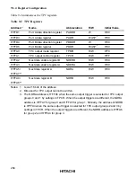
Table 9-2 summarizes the TPC registers.
Table 9-2 TPC Registers
Address
*
1
Name
Abbreviation
R/W
Initial Value
H'FFD1
Port A data direction register
PADDR
W
H'00
H'FFD3
Port A data register
PADR
R/(W)
*
2
H'00
H'FFD4
Port B data direction register
PBDDR
W
H'00
H'FFD6
Port B data register
PBDR
R/(W)
*
2
H'00
H'FFA0
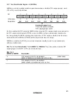
TPC output mode register
TPMR
R/W
H'F0
H'FFA1
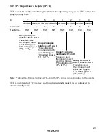
TPC output control register
TPCR
R/W
H'FF
H'FFA2
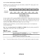
Next data enable register B
NDERB
R/W
H'00
H'FFA3
Next data enable register A
NDERA
R/W
H'00
H'FFA5/
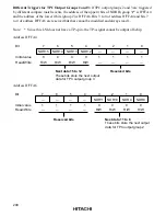
Next data register A
NDRA
R/W
H'00
H'FFA7
*
3
H'FFA4/
Next data register B
NDRB
R/W
H'00
H'FFA6
*
3
Notes: 1. Lower 16 bits of the address.
2. Bits used for TPC output cannot be written.
3. The NDRA address is H'FFA5 when the same output trigger is selected for TPC output
groups 0 and 1 by settings in TPCR. When the output triggers are different, the NDRA
address is H'FFA7 for group 0 and H'FFA5 for group 1. Similarly, the address of NDRB
is H'FFA4 when the same output trigger is selected for TPC output groups 2 and 3 by
settings in TPCR. When the output triggers are different, the NDRB address is H'FFA6
for group 2 and H'FFA4 for group 3.


