61
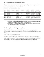
3.5 Pin Functions in Each Operating Mode
The pin functions of ports 1 to 3, port 5 and port A vary depending on the operating mode. Table
3-3 indicates their functions in each operating mode.
Table 3-3 Pin Functions in Each Mode
Port
Mode 1
Mode 2
*
1
Mode 3
Mode 4
*
1
Mode 5
Mode 6
Mode 7
Port 1
A
7
to A
0
—
A
7
to A
0
—
P1
7
to P1
0
*
2
P1
7
to P1
0
*
2
P1
7
to P1
0
Port 2
A
15
to A
8
—
A
15
to A
8
—
P2
7
to P2
0
*
2
P2
7
to P2
0
*
2
P2
7
to P2
0
Port 3
D
7
to D
0
—
D
7
to D
0
—
D
7
to D
0
D
7
to D
0
P3
7
to P3
0
Port 5
A
19
to A
16
—
A
19
to A
16
—
P5
3
to P5
0
*
2
P5
3
to P5
0
*
2
P5
3
to P5
0
Port A
PA
7
to PA
4
—
PA
6
to PA
4
*
3
,
A
20
—
PA
7
to PA
4
PA
6
to PA
4
*
3
,
A
20
PA
7
to PA
4
Notes: 1. H8/3022 Series cannot be used in these modes.
2. Initial state. These pins become address output pins when the corresponding bits in the
data direction registers (P1DDR, P2DDR, P5DDR) are set to 1.
3. Initial state A
20
is always an address output pin. PA
6
to PA
4
are switched over to A
23
to
A
21
output by writing 0 in bits 7 to 5 of ADRCR.
3.6 Memory Map in Each Operating Mode
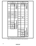
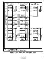
Figure 3-1 shows a memory map of the H8/3022. Figure 3-2 shows a memory map of the
H8/3021. Figure 3-3 shows a memory map of the H8/3020. The address space is divided into eight
areas.
Modes 1, 3, 5, and 6 are the 8-bit bus mode.
The address locations of the on-chip RAM and internal I/O registers differ between the 1-Mbyte
modes (modes 1, 5, and 7) and 16-Mbyte modes (mode 3 and 6). The address range specifiable by
the CPU in the 8- and 16-bit absolute addressing modes (@aa:8 and @aa:16) also differs.


