185
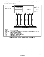
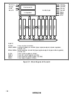
Block Diagram of Channels 0 and 1: ITU channels 0 and 1 are functionally identical. Both have
the structure shown in figure 8-2.
Clock selector
Comparator
Control logic
TCLKA to TCLKD
ø, ø/2, ø/4, ø/8
TIOCA
0
TIOCB
0
IMIA0
IMIB0
OVI0
TCNT
GRA
GRB
TCR
TIOR
TIER
TSR
Module data bus
Legend
TCNT:
GRA, GRB:
TCR:
TIOR:
TIER:
TSR:
Timer counter (16 bits)
General registers A and B (input capture/output compare registers) (16 bits 2)
Timer control register (8 bits)
Timer I/O control register (8 bits)
Timer interrupt enable register (8 bits)
Timer status register (8 bits)
×
Figure 8-2 Block Diagram of Channels 0 and 1 (for Channel 0)

