187
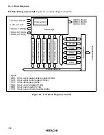
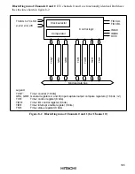
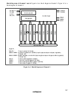
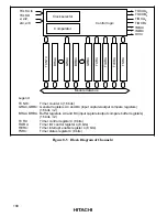
Block Diagrams of Channels 3 and 4: Figure 8-4 is a block diagram of channel 3. Figure 8-5 is a
block diagram of channel 4.
TCNT3
BRA3
Legend
TCNT3:
GRA3, GRB3:
BRA3, BRB3:
TCR3:
TIOR3:
TIER3:
TSR3:
Timer counter 3 (16 bits)
General registers A3 and B3 (input capture/output compare registers)
(16 bits 2)
Buffer registers A3 and B3 (input capture/output compare buffer registers)
(16 bits 2)
Timer control register 3 (8 bits)
Clock selector
Comparator
Control logic
GRA3
BRB3
GRB3
TCR3
TIOR3
TIER3
TSR3
TCLKA to
TCLKD
ø, ø/2,
ø/4, ø/8
TIOCA
3
TIOCB
3
Module data bus
×
IMIA3
IMIB3
OVI3
Timer I/O control register 3 (8 bits)
Timer interrupt enable register 3 (8 bits)
Timer status register 3 (8 bits)
×
Figure 8-4 Block Diagram of Channel 3


