53
T
, ,
AS
ø
1
T
2
Address bus
D
7
to D
0
RD WR
High
Address
High impedance
Figure 2-16 Pin States during On-Chip Memory Access
2.9.3 On-Chip Supporting Module Access Timing
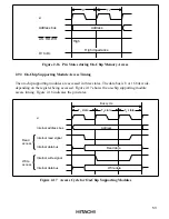
The on-chip supporting modules are accessed in three states. The data bus is 8 or 16 bits wide,
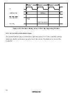
depending on the register being accessed. Figure 2-17 shows the on-chip supporting module
access timing. Figure 2-18 indicates the pin states.
Internal address bus
Internal read signal
Internal data bus
Internal write signal
Address
Internal data bus
ø
T state
Bus cycle
1
T state
2
T state
3
Read
access
Write
access
Write data
Read data
Figure 2-17 Access Cycle for On-Chip Supporting Modules


