479
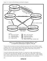
Flash memory access disabled period
(x: Wait time after SWE setting, y: Wait time after SWE clearing)
*
2
Flash memory reprogrammable period
(Flash memory program execution and data read, other than verify, are disabled.)
φ
V
CC
FWE
t
OSC1
Min. 0
µ
s
Min. 0
µ
s
Min.
200 ns
t
MDS
t
MDS
MD
2
to MD
0
*
1
RES
SWE bit
SWE
set
SWE
clear
Programming
and erase
possible
Wait time:
x
Wait time:
y
Notes: 1. Always fix the level by pulling down or pulling up the mode pins (MD
2
to MD
0
)
until powering off, except for mode switching.
2. See 18.2.5 Flash Memory Characteristics.
Figure 15-17 Powering On/Off Timing (Boot Mode)

