528
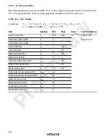
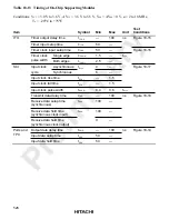
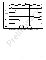
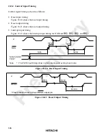
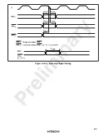
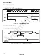
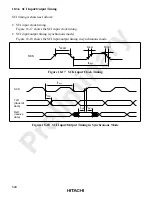
Table 18-13 Timing of On-Chip Supporting Modules
Conditions: V
CC
= 3.0 V to 3.6 V, AV
CC
= 3.6 V to 5.5 V, V
SS
= AV
SS
= 0 V, ø = 2 to 18 MHz,
T
a
= –20
°
C to +75
°
C
Item
Symbol
Min
Max
Unit
Test
Conditions
ITU
Timer output delay time
t
TOCD
—
100
ns
Figure 18-15
Timer input setup time
t
TICS
50
—
Timer clock input setup time
t
TCKS
50
—
Figure 18-16
Timer clock
Single edge
t
TCKWH
1.5
—
t
cyc
pulse width
Both edges
t
TCKWL
2.5
—
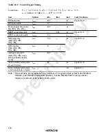
SCI
Input clock
Asynchronous
t
Scyc
4
—
Figure 18-17
cycle
Synchronous
6
—
Input clock rise time
t
SCKr
—
1.5
Input clock fall time
t
SCKf
—
1.5
Input clock pulse width
t
SCKW
0.4
0.6
t
Scyc
Transmit data delay time
t
TXD
—
100
ns
Figure 18-18
Receive data setup time
(synchronous)
t
RXS
100
—
Receive data hold time
(synchronous clock input)
t
RXH
100
—
Receive data hold time
(synchronous clock output)
0
—
Ports and
Output data delay time
t
PWD
—
100
ns
Figure 18-14
TPC
Input data setup time
t
PRS
50
—
Input data hold time
t
PRH
50
—

