336
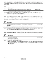
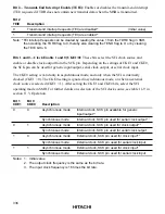
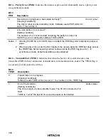
Bit 2—Transmit-End Interrupt Enable (TEIE): Enables or disables the transmit-end interrupt
(TEI) requested if TDR does not contain new transmit data when the MSB is transmitted.
Bit 2
TEIE
Description
0
Transmit-end interrupt requests (TEI) are disabled
*
(Initial value)
1
Transmit-end interrupt requests (TEI) are enabled
*
Note:
*
TEI interrupt requests can be cleared by reading the value 1 from the TDRE flag in SSR,
then clearing the TDRE flag to 0, thereby also clearing the TEND flag to 0; or by clearing
the TEIE bit to 0.
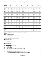
Bits 1 and 0—Clock Enable 1 and 0 (CKE1/0): These bits select the SCI clock source and
enable or disable clock output from the SCK pin. Depending on the settings of CKE1 and CKE0,
the SCK pin can be used for generic input/output, serial clock output, or serial clock input.
The CKE0 setting is valid only in asynchronous mode, and only when the SCI is internally
clocked (CKE1 = 0). The CKE0 setting is ignored in synchronous mode, or when an external
clock source is selected (CKE1 = 1). After setting the CKE1 and CKE0 bits, select the SCI
operating mode in SMR. For further details on selection of the SCI clock source, see table 11-9 in
section 11.3, Operation.
Bit 1
CKE1
Bit 0
CKE0
Description
0
0
Asynchronous mode
Internal clock, SCK pin available for generic
input/output
*
1
Synchronous mode
Internal clock, SCK pin used for serial clock output
*
1
0
1
Asynchronous mode
Internal clock, SCK pin used for clock output
*
2
Synchronous mode
Internal clock, SCK pin used for serial clock output
1
0
Asynchronous mode
External clock, SCK pin used for clock input
*
3
Synchronous mode
External clock, SCK pin used for serial clock input
1
1
Asynchronous mode
External clock, SCK pin used for clock input
*
3
Synchronous mode
External clock, SCK pin used for serial clock input
Notes: 1. Initial value
2. The output clock frequency is the same as the bit rate.
3. The input clock frequency is 16 times the bit rate.

