525
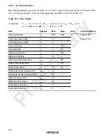
18.2.3 AC Characteristics
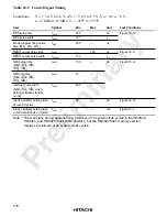
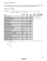
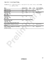
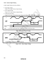
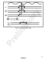
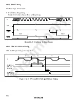
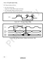
Bus timing parameters are listed in table 18-11. Control signal timing parameters are listed in table
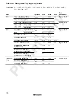
18-12. Timing parameters of the on-chip supporting modules are listed in table 18-13.
Table 18-11 Bus Timing
Conditions: V
CC
= 3.0 V to 3.6 V, AV
CC
= 3.6 V to 5.5 V, V
SS
= AV
SS
= 0 V,
ø = 2 MHz to 18 MHz, T
a
= –20
°
C to +75
°
C
Item
Symbol
Min
Max
Unit
Test Conditions
Clock cycle time
t
cyc
55.5
500
ns
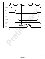
Figure 18-7,
Clock low pulse width
t
CL
17
—
Figure 18-8
Clock high pulse width
t
CH
17
—
Clock rise time
t
Cr
—
10
Clock fall time
t
Cf
—
10
Address delay time
t
AD
—
25
Address hold time
t
AH
10
—
Address strobe delay time
t
ASD
—
25
Write strobe delay time
t
WSD
—
25
Strobe delay time
t
SD
—
25
Write data strobe pulse width 1
t
WSW1
*
32
—
Write data strobe pulse width 2
t
WSW2
*
62
—
Address setup time 1
t
AS1
10
—
Address setup time 2
t
AS2
38
—
Read data setup time
t
RDS
15
—
Read data hold time
t
RDH
0
—

