198
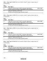
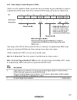
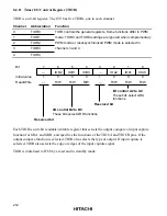
When MDF is set to 1 to select phase counting mode, timer counter 2 (TCNT2) operates as an
up/down-counter and pins TCLKA and TCLKB become counter clock input pins. TCNT2 counts
both rising and falling edges of TCLKA and TCLKB, and counts up or down as follows.
Counting Direction
Down-Counting
Up-Counting
TCLKA pin
High
Low
Low
High
TCLKB pin
Low
High
High
Low
In phase counting mode channel 2 operates as above regardless of the external clock edges
selected by bits CKEG1 and CKEG0 and the clock source selected by bits TPSC2 to TPSC0 in
timer control register 2 (TCR2). Phase counting mode takes precedence over these settings.
The counter clearing condition selected by the CCLR1 and CCLR0 bits in TCR2 and the compare
match/input capture settings and interrupt functions of timer I/O control register 2 (TIOR2), timer
interrupt enable register 2 (TIER2), and timer status register 2 (TSR2) remain effective in phase
counting mode.
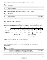
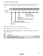
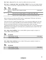
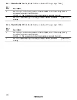
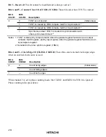
Bit 5—Flag Direction (FDIR): Designates the setting condition for the overflow flag (OVF) in
timer status register 2 (TSR2). The FDIR designation is valid in all modes in channel 2.
Bit 5
FDIR
Description
0
OVF is set to 1 in TSR2 when TCNT2 overflows or underflows
(Initial value)
1
OVF is set to 1 in TSR2 when TCNT2 overflows
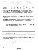
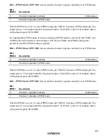
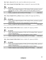
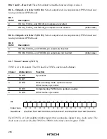
Bit 4—PWM Mode 4 (PWM4): Selects whether channel 4 operates normally or in PWM mode.
Bit 4
PWM4
Description
0
Channel 4 operates normally
(Initial value)
1
Channel 4 operates in PWM mode
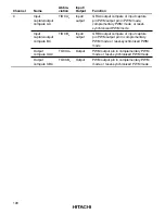
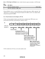
When bit PWM4 is set to 1 to select PWM mode, pin TIOCA4 becomes a PWM output pin. The
output goes to 1 at compare match with general register A4 (GRA4), and to 0 at compare match
with general register B4 (GRB4).
If complementary PWM mode or reset-synchronized PWM mode is selected by bits CMD1 and
CMD0 in the timer function control register (TFCR), the CMD1 and CMD0 setting takes
precedence and the PWM4 setting is ignored.

