125
6.4 Usage Notes
6.4.1 Register Write Timing
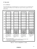
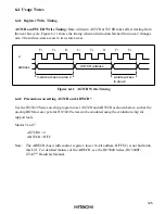
ASTCR and WCER Write Timing: Data written to ASTCR or WCER takes effect starting from
the next bus cycle. Figure 6-11 shows the timing when an instruction fetched from area 2 changes
area 2 from three-state access to two-state access.
ø
Address
T
1
T
2
T
3
T
1
T
2
T
3
T
1
T
2
ASTCR address
3-state access to area 2
2-state access
to area 2
Figure 6-11 ASTCR Write Timing
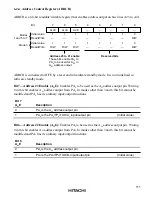
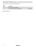
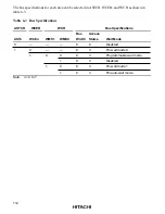
6.4.2 Precautions on setting ASTCR and ABWCR*
Use the H8/3022 Series on-chip program to set ASTCR and ABWCR as shown below, so that the
on-chip ROM access cycle for H8/3022 Series can be emulated using the evaluation chip for
support tools.
Modes 5 and 7
ASTCR0 = 0
ABWCR = H'FC
Note:
The ABWCR (bus width control register; lower 16-bit address: H'FFEC) is not built onto
this LSI. For detailed features of the ABWCR, see the H8/3048 Series, H8/3048F-
ZTAT
TM
Hardware Manual.

