427
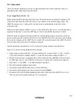
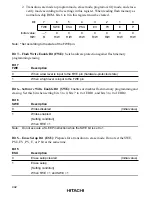
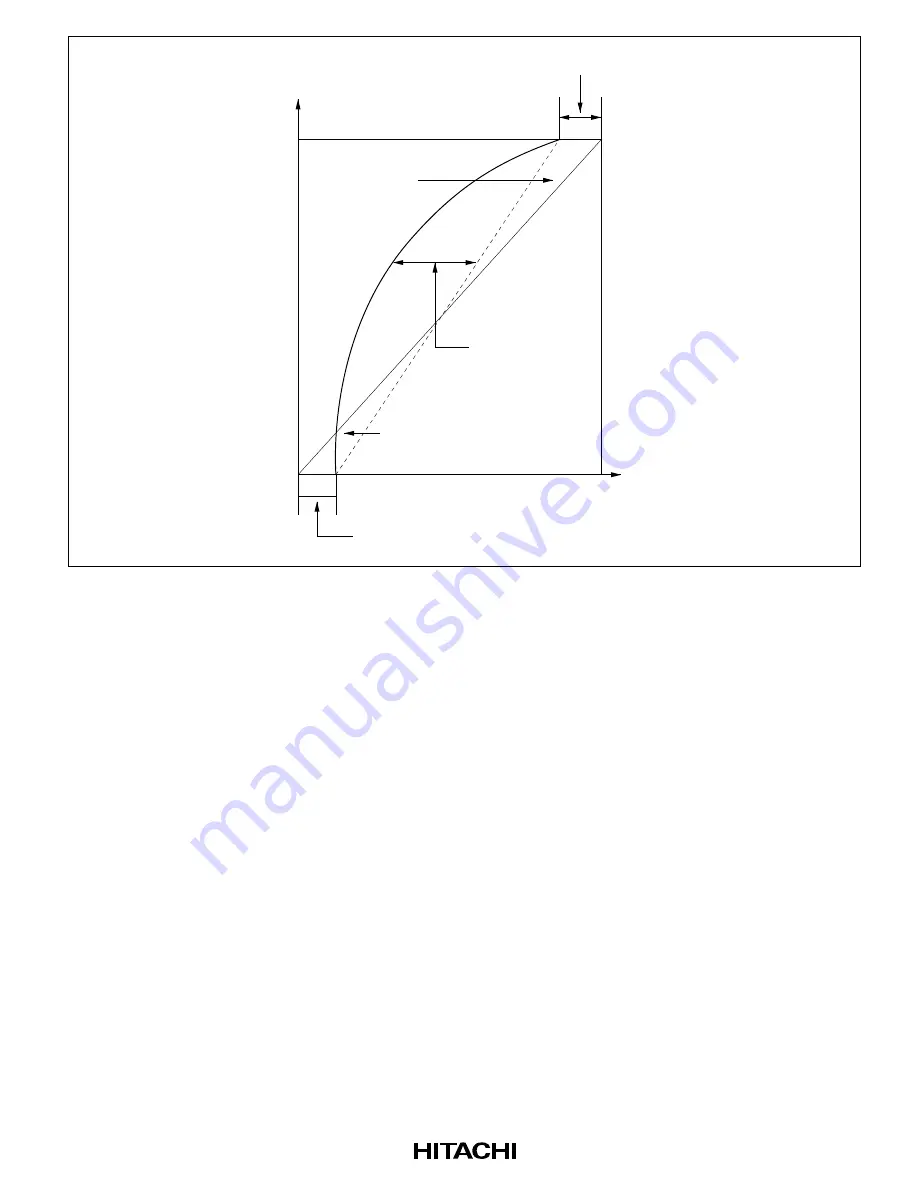
FS
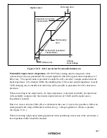
Offset error
Nonlinearity
error
Actual A/D conversion
characteristic
Analog
input voltage
Digital output
Ideal A/D conversion
characteristic
Full-scale error
Figure 13-10 A/D Conversion Precision Definitions (2)
Permissible Signal Source Impedance: H8/3022 Series analog input is designed so that
conversion precision is guaranteed for an input signal for which the signal source impedance is 5
k
Ω
or less. This specification is provided to enable the A/D converter’s sample-and-hold circuit
input capacitance to be charged within the sampling time; if the sensor output impedance exceeds
5 k
Ω
, charging may be insufficient and it may not be possible to guarantee the A/D conversion
precision.
When converting in the single mode, if a large capacitance is provided externally, the input load
will essentially comprise only the internal input resistance of 10 k
Ω
, and the signal source
impedance is ignored.
However, since a low-pass filter effect is obtained in this case, it may not be possible to follow an
analog signal with a large differential coefficient (e.g., voltage regulation 5 mV/
µ
s or greater).
(See figure 13-11.)
When converting a high-speed analog signal and when performing conversion in the scan mode, a
low-impedance buffer should be inserted.

