131
7.2 Port 1
7.2.1 Overview
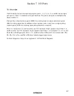
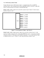
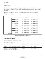
Port 1 is an 8-bit input/output port with the pin configuration shown in figure 7-1. The pin
functions differ between the expanded modes with on-chip ROM disabled, expanded modes with
on-chip ROM enabled, and single-chip mode. In modes 1, 3 (expanded modes with on-chip ROM
disabled), they are address bus output pins (A
7
to A
0
).
In modes 5 and 6 (expanded modes with on-chip ROM enabled), settings in the port 1 data
direction register (P1DDR) can designate pins for address bus output (A
7
to A
0
) or generic input.
In mode 7 (single-chip mode), port 1 is a generic input/output port.
Pins in port 1 can drive one TTL load and a 90-pF capacitive load. They can also drive a
Darlington transistor pair.
Port 1
P1 /A
P1 /A
P1 /A
P1 /A
P1 /A
P1 /A
P1 /A
P1 /A
7
6
5
4
3
2
1
0
7
6
5
4
3
2
1
0
P1 (input/output)
P1 (input/output)
P1 (input/output)
P1 (input/output)
P1 (input/output)
P1 (input/output)
P1 (input/output)
P1 (input/output)
7
6
5
4
3
2
1
0
A (output)
A (output)
A (output)
A (output)
A (output)
A (output)
A (output)
A (output)
7
6
5
4
3
2
1
0
Port 1 pins
Mode 7
Modes 1 and 3
P1 (input)/A (output)
P1 (input)/A (output)
P1 (input)/A (output)
P1 (input)/A (output)
P1 (input)/A (output)
P1 (input)/A (output)
P1 (input)/A (output)
P1 (input)/A (output)
7
6
5
4
3
2
1
0
Modes 5 and 6
7
6
5
4
3
2
1
0
Figure 7-1 Port 1 Pin Configuration
7.2.2 Register Descriptions
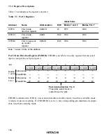
Table 7-2 summarizes the registers of port 1.

