104
YASKAWA
SIEPYAIH6B01A HV600 AC Drive Bypass Technical Reference
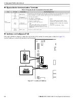
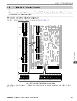
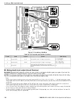
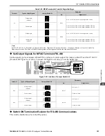
Figure 3.18 Locations of Switches
Table 3.25 I/O Terminals and Switches Functions
Position
Switch
Terminal
Function
Default Setting
A
Jumper switch S1
A1, A2
Sets terminals A1 and A2 to voltage or current output.
A1: V (voltage input)
A2: I (current input)
B
Jumper switch S5
FM, AM
Sets terminals FM and AM to voltage or current output.
FM: V (voltage output)
AM: V (voltage output)
C
DIP switch S2
-
Enables and disables the termination resistor of embedded
communications protocols. This switch should always be in the ON
position.
ON
◆
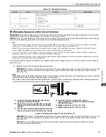
Wiring the Drive Control Circuit Terminal
WARNING!
Electrical Shock Hazard. Do not remove covers or touch circuit boards while the bypass is energized. If you touch the
internal components of an energized bypass, it can cause serious injury or death.
NOTICE:
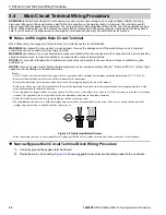
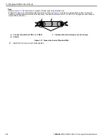
Do not let wire shields touch other signal lines or equipment. Insulate the wire shields with electrical tape or shrink tubing.
If you do not insulate the wire shields, it can cause a short circuit and damage the drive.
Note:
•
Isolate control circuit wiring from main circuit wiring (terminals R/L1, S/L2, T/L3, U/T1, V/T2, W/T3, -, +1) and other high-power wiring.
If the control circuit wires are adjacent to the main circuit wires, electrical interference can cause the drive or the devices around the drive to
malfunction.
•
Isolate contact output terminals MA, MB, MC and M1-M6 from other control circuit wiring. If the output terminal wires are adjacent to
other control circuit wires, electrical interference can cause the drive or devices around the drive to malfunction.
•
Use a UL Listed Class 2 Power Supply to connect external power to the contact output control terminals. If the power supply for peripheral
devices is incorrect, it can cause a decrease in drive performance.
•
Connect the shield of shielded cable to the applicable ground terminal. If the grounding is not correct, electrical interference can cause the
drive or devices around the drive to malfunction.
Содержание H6B1A002
Страница 2: ...This Page Intentionally Blank 2 YASKAWA SIEPYAIH6B01A HV600 AC Drive Bypass Technical Reference...
Страница 12: ...12 YASKAWA SIEPYAIH6B01A HV600 AC Drive Bypass Technical Reference...
Страница 30: ...1 2 Catalog Code and Nameplate Check 30 YASKAWA SIEPYAIH6B01A HV600 AC Drive Bypass Technical Reference...
Страница 68: ...2 9 Knock Out Hole Dimensions 68 YASKAWA SIEPYAIH6B01A HV600 AC Drive Bypass Technical Reference...
Страница 74: ...Page Intentionally Blank...
Страница 76: ...Page Intentionally Blank...
Страница 454: ...5 14 Z Bypass Parameters 454 YASKAWA SIEPYAIH6B01A HV600 AC Drive Bypass Technical Reference...
Страница 590: ...8 6 Storage Guidelines 590 YASKAWA SIEPYAIH6B01A HV600 AC Drive Bypass Technical Reference...
Страница 694: ...9 19 Defaults by Bypass and Drive Model 694 YASKAWA SIEPYAIH6B01A HV600 AC Drive Bypass Technical Reference...
Страница 768: ...10 6 MEMOBUS Modbus Communications 768 YASKAWA SIEPYAIH6B01A HV600 AC Drive Bypass Technical Reference...
Страница 780: ...11 3 European Standards 780 YASKAWA SIEPYAIH6B01A HV600 AC Drive Bypass Technical Reference...

