11
11-42
Ver.0.10
11.3.2 A-D Conversion by Successive Approximation Method
The A-D converter has A-D convert operation started by an A-D conversion start trigger (in software
or hardware). Once A-D conversion begins, the following operation is automatically executed.
➀
During single mode, Single Mode Register 0's A-D conversion/comparate completion bit is
cleared to 0. During scan mode, Can Mode Register 0's A-D conversion completion bit is
cleared to 0.
➁
The content of the A-D Successive Approximation Register is cleared to "H'0000."
➂
The A-D Successive Approximation Register's most significant bit (D6) is set to 1.
➃
The comparison voltage, Vref(note), is fed from the D-A converter into the comparator.
➄
The comparison voltage, Vref, and the analog input voltage, VIN, are compared, with the
comparison result stored in D6.
If Vref < VIN, then D6 = 1
If Vref > VIN, then D6 = 0
➅
Operations in steps
➂
through
➄
above are executed for all other bits from D7 to D15.
➆
The value stored in the A-D Successive Approximation Register at completion of the
comparison of D15 is the final A-D conversion result.
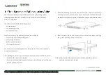
Figure 11.3.2 Changes of the A-D Successive Approximation Register during A-D Convert Operation
Note: The comparison voltage, Vref (the voltage fed from the D-A converter into the comparator), is
determined according to changes of the content of the A-D Successive Approximation Register. Shown
below are the equations used to calculate the comparison voltage, Vref.
• When the content of the A-D Successive Approximation Register = 0
Vref [V] = 0
• When the content of the A-D Successive Approximation Register = 1 to 1,023
Vref [V] = (reference voltage VREF / 1,024) x (content of the A-D Successive Approximation Register - 0.5)
A-D CONVERTERS
11.3 Functional Description of A-D Converters
1st comparison
D6
7
8
9
10
11
12
13
14
D15
1
0
0
0
0
0
0
0
0
0
n9
1
0
0
0
0
0
0
0
0
n9
n8
1
0
0
0
0
0
0
0
n9
n8
n7
n6
n5
n4
n3
n2
n1
1
2nd comparison
3rd comparison
10th comparison
Conversion
completed
n9
n8
n7
n6
n5
n4
n3
n2
n1
n0
Result of 1st comparison
Result of 2nd comparison
Vref > VIN then nX=0
Vref < VIN then nX=1
A-D Successive Approximation Register (ADiSAR) i=0,1
Summary of Contents for M32170F3VFP
Page 42: ...1 1 24 Ver 0 10 OVERVIEW 1 4 Pin Layout This is a blank page ...
Page 56: ...2 2 14 Ver 0 10 This is a blank page ...
Page 88: ...3 3 32 Ver 0 10 ADDRESS SPACE 3 7 Notes on Address Space This is a blank page ...
Page 270: ...9 9 40 Ver 0 10 DMAC 9 4 Precautions about the DMAC This is a blank page ...
Page 614: ...12 12 64 Ver 0 10 This is a blank page SERIAL I O 12 9 Precautions on Using UART Mode ...
Page 756: ...17 17 10 Ver 0 10 RAM BACKUP MODE 17 4 Exiting RAM Backup Mode Wakeup This is a blank page ...
Page 762: ...18 18 6 Ver 0 10 OSCILLATION CIRCUIT 18 2 Clock Generator Circuit This is a blank page ...
Page 831: ...CHAPTER 22 CHAPTER 22 TYPICAL CHARACTERISTICS 22 1 A D Conversion Characteristics ...
Page 833: ...Appendix 1 1 Dimensional Outline Drawing APPENDIX 1 APPENDIX 1 MECHANICAL SPECIFICATIONS ...
Page 841: ...Appendix 3 1 Precautions about Noise APPENDIX 3 APPENDIX 3 PRECAUTIONS ABOUT NOISE ...