ADwin-Pro
Hardware, manual version 2.9, June 2006
171
Pro I: Signal Conditioning and Interface Modules
Pro-CAN-x Rev. A
ADwin
2 CAN interfaces
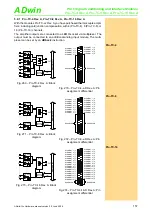
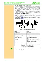
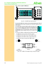
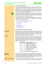
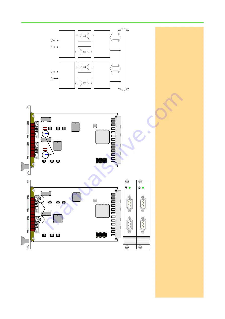
Fig. 302 – Pro-CAN-2: Block diagram for 2 interfaces
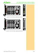
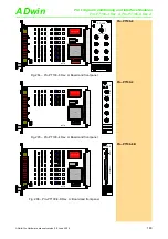
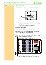
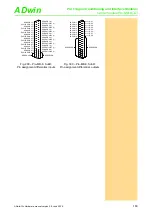
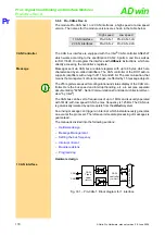
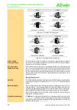
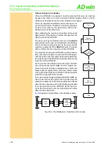
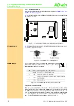
Fig. 303 – Pro-CAN-1/-2: PCB and front panels
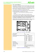
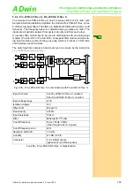
The connections of the CAN bus interface are on the 9-pin D-SUB connector;
the pin assignment is shown below. On the CAN-1 and CAN-1-LS modules
both D-SUB connectors are internally connected with each other.
ADwin-Pro
bus
+
-
CAN
H
CAN-
controller
(intel 82527)
EVENT
CAN-
Trans-
ceiver
(82C250)
CAN
L
Data
+
-
CAN
H
CAN-
controller
(intel 82527)
EVENT
CAN-
Trans-
ceiver
(82C250)
CAN
L
Data
19CAN01
OCX
FPGA
ON
DIP
1
2
3
4
5
6
7
8
CAN
Controller
82527
Intel
®
AN82527
DCP010505BP
PC
A8
2
C
250
721
721
CAN
Controller
82527
Intel
®
AN82527
PC
A8
2
C
250
721
721
ON OFF
Term.
ON OFF
Term.
DCP010505BP
A0 A1 A2 A3 A4 A5 A6 A7
Jumper Bus Termination
Rev. A1
CAN-2
CAN PORT
1
2
19CAN02
OCX
FPGA
ON
DIP
1
2
3
4
5
6
7
8
Intel
®
AN82527
DCP010505BP
PC
A8
2
C
250
721
721
Intel
®
AN82527
PC
A8
2
C
250
721
721
ON
OFF
Term.
ON
OFF
Term.
DCP010505BP
A0 A1 A2 A3 A4 A5 A6 A7
CAN-1
CAN PORT
1.1
1.2
DIP Switch Bus Termination
since Rev. A2

