Pro I: Analog Input Modules
Pro-AIn-F-8/12 Rev. A
ADwin
68
ADwin-Pro
Hardware, manual version 2.9, June 2006
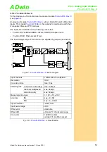
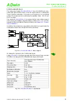
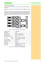
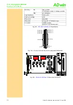
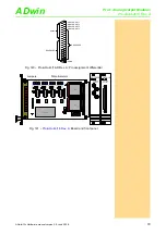
Fig. 119 – Pro-AIn-F-8/12-D Rev. A: Pin assignment differential
Fig. 120 –
: Board and front panel
Setting Offset and Gain factor
The analog input modules
and
are equipped with each 4 ADC, the modules
and
with each 8 ADC. The ADC 1 to 4 are on the base PCB
and the ADC 5 to 8 are on an additional PCB which will be plugged into the
base PCB. The input voltage of the ADC is fixed to ±10V.
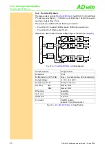
The potentiometers Ox and Gx are used for an accurate adjustment of gain
and offset (
). The "x" in the potentiometer’s names stands for the num-
ber of the corresponding ADC. The potentiometer names are printed on the
boards.
When testing the modules, the potentiometers have been optimally adjusted.
Therefore we ask you to avoid adjusting the potentiometers if not necessary,
because this may result in inaccuracy. The calibration of the ADC is described
in the
.
ANALOG IN 1 (-)
ANALOG IN 2 (-)
ANALOG IN 3 (-)
ANALOG IN 4 (-)
ANALOG IN 5 (-)
ANALOG IN 6 (-)
ANALOG IN 7 (-)
ANALOG IN 8 (-)
AGND
RESERVED
ANALOG IN 1 (+)
ANALOG IN 2 (+)
ANALOG IN 3 (+)
ANALOG IN 4 (+)
ANALOG IN 5 (+)
ANALOG IN 6 (+)
ANALOG IN 7 (+)
ANALOG IN 8 (+)
AGND
RESERVED
DGND
19
18
17
16
15
14
13
12
11
10
9
8
7
6
5
4
3
2
1
37
36
35
34
33
32
31
30
29
28
27
26
25
24
23
22
21
20
RESERVED
RESERVED
FP
G
A
FP
G
A
19AD976A
ON
1 2 3 4 5 6 7 8
A0 A1 A2 A3 A4 A5 A6 A7
LS19
OCX
DC/DC-converter
O4
G4
O2
G2
O3
G3
O1
G1
IN
A
103
LT
C
1410
IN
A
103
LT
C
1410
IN
A
103
LT
C
1410
IN
A
103
LT
C
1410
DC/DC-converter
O8
G8
O6
G6
O7
G7
O5
G5
IN
A
103
LT
C
1410
IN
A
103
LT
C
1410
IN
A
103
LT
C
1410
IN
A
103
LT
C
1410
19AD976B
AIN-F8/12
ANALOG
INPUT
1
2
3
4
5
6
7
8
AIN-F8/12
ANALOG
INPUT
Potentiometers
Potentiometer
Adjustment of
Gx
Gain factor
Ox
Offset
Fig. 121 –
: Function of the potentiometers


