


NOVA electronics Inc.
MCX514 -
97
-
97
-
■
Interrupt in 8-bit data bus
When 8-bit data bus is used, individually set each WR1H/WR1L register to 1– enable or 0 – disable. When an interrupt occurs
(interrupt signal (INT0N) is Low), individually read each RR1H/ RR1L register. If either register is only enabled, there is no need
to read another register. The bits that indicate an interrupt are cleared to 0 by reading RR1H register once and RR1L register is the
same as RR1H. When all the bits of both registers are cleared, the interrupt signal (INT0N) returns to the Hi-Z level.
■
Interrupt in
I
2
C
serial interface bus
When I
2
C serial interface bus is used, individually set each WR1H/WR1L register to 1– enable or 0 – disable. In addition, it can
be set to 1– enable or 0 – disable by WR1 registers at once. When an interrupt occurs (interrupt signal (INT0N) is Low), read RR1
registers. Even though either register is only enabled, be sure to read 2 bytes (RR1L, RR1H). When RR1 register is read out, the
bits that indicate an interrupt are cleared to 0 and the interrupt signal (INT0N) returns to the Hi-Z level.
For more details of I
2
C serial interface bus, see chapter 4, details of WR1 register, see chapter 6.5 and details of RR1 register, see
chapter 6.12
Notes on the read timing from CPU
The timing of read/write cycles from the CPU is shown in chapter 10.2.2. In read cycle, the address signal A[3:0] must be
determined in the section of RDN signal is Low level. tAR minimum is 0 and tRA minimum is 3nsec. If this condition is violated
and non-valid address data is into the section of RDN signal is Low level, the data of RR1 register will be cleared by reading the
other register and the interrupt signal (INT0N) may be cleared. Please note the read timing from the CPU when using the interrupt
signal (INT0N).
2.10.2 Interrupt during Continuous Interpolation
It sets to 1– enable or 0 – disable by interpolation mode setting command (2Ah). When the interrupt factor that is enabled becomes
True, interpolation interrupt output signal (INT1N) becomes Low level.
Table 2.10-2 Interrupt Factor generated in Continuous Interpolation
Enable / Disable
Interpolation Mode
Factors of Interrupt
D14 (INTA)
Stack counter in pre buffer changed from 4 to 3.
D15 (INTB)
Stack counter in pre buffer changed from 8 to 7.
Interpolation interrupt output signal (INT1N) is cleared and returns to the Hi-Z level by the following condition.
①
Interpolation interrupt clear command (6Fh) is written.
②
Interpolation execution command of next segment is written.
③
Continuous interpolation driving is finished.
When both interrupt factors are enabled, if the first interrupt factor becomes True, interpolation interrupt output signal (INT1N)
will be on the Low level. After that, if the other interrupt factor becomes True before clearing, interpolation interrupt output signal
(INT1N) keeps the Low level. And if they are cleared, interpolation interrupt output signal (INT1N) returns to the Hi-Z level.
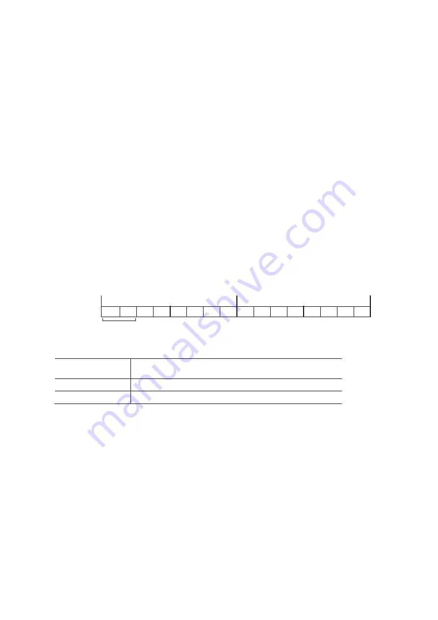
D7
D6
D5
D4
H
L
D15
D14
D13
D12
D11
D10
D9
D8
D3
D2
D1
D0
WR6
INTA
INTB
Interpolation driving Interrupt


