Chapter XVIII Working Principle
229
Power module
CH1
Channel signal
adjustment
5GSa/s
A/D converter
(ADC1)
Clock phase lock
and distribution
FPGA
Embedde
d CPU
DDR3
Keyboard
Power supply
AC/DC
220V
50Hz
CH2
Channel signal
adjustment
CH3
Channel signal
adjustment
CH4
Channel signal
adjustment
AUX IN
External trigger
adjustment
Clock selection
REFIN/OUT
5GSa/s
A/D converter
(ADC2)
FPGA
DDR3
Acquisition and storage
Waveform processing
Waveform processing
Acquisition and storage
Digital trigger
Fluorescence image
synthesis
Comm
unicati
on
interfa
ce
interac
tion
Function generator
(Option 002)
Logic analyzer (option 001)
CH_1
CH_2
CH_3
CH_4
Capacitive touch screen
LCD display
LAN
(
1
)
Main USB (4)
Slave USB (1)
VGA
AUX OUT
Output
Video decoder
CH_1
CH_2
CH_3
CH_4
mains
DC/DC
LDO
10MHz
2.5GHz
2.5GHz
10MH
z
10MHz
10MHz
Bus
Trigger and analysis
16-channel logic analyzer input
Any Acquire phosphor technology
Digital trigger
Display control
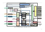
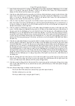
Fig. 18.1 Principle Block Diagram of Digital Phosphor Oscilloscope
Summary of Contents for 4456 Series
Page 10: ...VIII...
Page 55: ...Chapter V Trigger System 45 Fig 5 51 RF Test Signal Example...
Page 69: ...Chapter VII Mathematical Operation 59 Fig 7 10 Advanced Math Example...
Page 71: ...Chapter VIII Display System 61 Fig 8 3 Wfm Palette Menu Fig 8 4 Normal Palette...
Page 72: ...Chapter VIII Display System 62 Fig 8 5 Inverted Palette Fig 8 6 Temperature Palette...
Page 75: ...Chapter VIII Display System 65 Fig 8 12 XY Display Example...
Page 165: ...Chapter XI Protocol Analyzer Option 155 Fig 11 242 1553 Trigger and Analysis Example...


