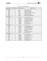


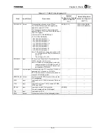


Chapter 5 Configuration Registers
5-11
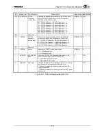
5.2.5
Clock Control Register (CLKCTR)
0xE020
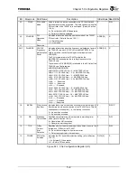
Bit 32 and bits 15-0 are reset bits for the on-chip peripheral modules. To bring on-chip peripheral
modules out of the reset state, the corresponding bits must be cleared by software. Before clearing them,
wait at least 128 CPU clock cycles after they are set.
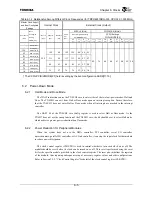
63
48
Reserved
: Type
: Initial value
47
32
Reserved
: Type
: Initial value
31
26 25 24 23 22 21 20 19 18 17 16
DMA1CKD
ACLCKD PIOCKD DMACKD PCICCKD
1 TM0CKD TM1CKD TM2CKD
SIO0CKD
SIO1CKD
R/W R/W R/W R/W R/W R/W R/W R/W R/W R/W R/W
:
Type
0 0 0 0 0 1 0 0 0 0 0
:
Initial
value
15 10 9 8 7 6 5 4 3 2 1 0
Reserved
DMA1RST
ACLRST
PIORST
DMA0RST
PCICRST
1
TM0RST TM1RST TM2RST SIO0RST SIO1RST
R/W
R/W R/W R/W R/W R/W R/W R/W R/W R/W R/W
: Type
0 0 0 0 0 1 0 0 0 0 0
:
Initial
value
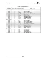
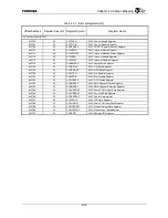
Bit
Mnemonic Field Name
Description
Initial Value Read/Write
63:27
⎯
Reserved
⎯
⎯
⎯
26 DMA1CKD
DMAC1 Clock
Disable
Controls clock pulses for the DMA controller 1.
0 = Supply clock pulses.
1 = Do not supply clock pulses.
0 R/W
25 ACLCKD
ACLC Clock
Disable
Controls clock pulses for the AC-link controller.
0 = Supply clock pulses.
1 = Do not supply clock pulses.
0 R/W
24 PIOCKD
PIO Clock
Disable
Controls clock pulses for the parallel IO controller.
0 = Supply clock pulses.
1 = Do not supply clock pulses.
0 R/W
23 DMA0CKD
DMAC0 Clock
Disable
Controls clock pulses for the DMA controller 0.
0 = Supply clock pulses.
1 = Do not supply clock pulses.
0 R/W
22 PCICKD
PCIC
Clock
Disable
Controls clock pulses for the PCI controller.
0 = Supply clock pulses.
1 = Do not supply clock pulses.
0 R/W
21
⎯
⎯
Always set this bit to 1.
1
R/W
20 TM0CKD
Timer 0 Clock
Disable
Controls clock pulses for the TMR0 controller.
0 = Supply clock pulses.
1 = Do not supply clock pulses.
0 R/W
19 TM1CKD
Timer 1 Clock
Disable
Controls clock pulses for the TMR1 controller.
0 = Supply clock pulses.
1 = Do not supply clock pulses.
0 R/W
18 TM2CKD
Timer 2 Clock
Disable
Controls clock pulses for the TMR2 controller.
0 = Supply clock pulses.
1 = Do not supply clock pulses.
0 R/W
Figure 5.2.5 Clock Control Register (1/2)
Содержание TX49 TMPR4937
Страница 1: ...64 Bit TX System RISC TX49 Family TMPR4937 Rev 2 0 ...
Страница 4: ......
Страница 13: ...Table of Contents ix TMPR4937 Revision History 1 ...
Страница 14: ...Table of Contents x ...
Страница 15: ...Handling Precautions ...
Страница 16: ......
Страница 18: ...1 Using Toshiba Semiconductors Safely 1 2 ...
Страница 40: ...3 General Safety Precautions and Usage Considerations 3 18 ...
Страница 42: ...4 Precautions and Usage Considerations 4 2 ...
Страница 43: ...TMPR4937 2005 3 Rev 2 0 ...
Страница 44: ......
Страница 52: ...Chapter 1 Overview and Features 1 6 ...
Страница 156: ...Chapter 7 External Bus Controller 7 56 ...
Страница 491: ...Chapter 16 Removed 16 1 16 Removed ...
Страница 492: ...Chapter 16 Removed 16 2 ...
Страница 493: ...Chapter 17 Removed 17 1 17 Removed ...
Страница 494: ...Chapter 17 Removed 17 2 ...
Страница 495: ...Chapter 18 Removed 18 1 18 Removed ...
Страница 496: ...Chapter 18 Removed 18 2 ...
Страница 497: ...Chapter 19 Removed 19 1 19 Removed ...
Страница 498: ...Chapter 19 Removed 19 2 ...
Страница 506: ...Chapter 20 Extended EJTAG Interface 20 8 ...
Страница 529: ...Chapter 22 Pinout and Package Information 22 9 22 2 Package Dimensions P BGA484 3535 1 27B9 Unit mm ...
Страница 530: ...Chapter 22 Pinout and Package Information 22 10 ...
Страница 542: ...Chapter 24 Parts Number when Ordering 24 2 ...
Страница 544: ...Appendix A TX49 H3 Core Supplement A 2 ...


