


Chapter 12 Timer/Counter
12-6
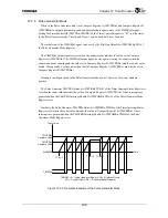
12.3.5 Pulse
Generator
Mode
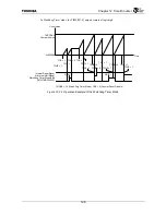
When in the Pulse Generator mode, use Compare Register A (TMCPRAn) and Compare Register B
(TMCPRBn) to output a particular period and particular duty square wave to the TIMER[n] signal.
Setting the Timer Mode field (TMTCRn.TMODE) of the Timer Control Register to “01” sets the timer
to the Pulse Generator mode. Timer 0 and Timer 1 can be used, but Timer 2 cannot.
The initial state of the TIMER[n] signal can be set by the Flip Flop Default bit (TMPGMRn.FFI) of
the Pulse Generator Mode Register.
The TIMER[n] output signal reverses when the counter value matches the value set in Compare
Register A (TMCPRAn). The TIMER[n] output signal reverse again, clearing the counter when the
counter continues counting and the value set in Compare Register B (TMCPRBn) and the counter value
match. Consequently, a value greater than that in Compare Register A (TMCPRAn) must not be set in
Compare Register B (TMCPRBn).
Interrupts can be generated in the Pulse Generator mode as well. However, this is not standard
practice.
The Pulse Generator TMCPRA Status bit (TMTISRn.TPIAS) of the Timer Interrupt Status Register is
set when the count value matches the value of Compare Register A (TMCPRAn). Timer interrupts are
generated when the TMCPRA Interrupt Enable bit (TMPGMRn.TPIAE) of the Pulse Generator Mode
Register is set.
Similarly, the Pulse Generator TMCPRB Status bit (TMTISRn.TPIBS) of the Timer Interrupt Status
Register is set when the count value matches the value of Compare Register B (TMCPRBn). Timer
interrupts are generated when the TMCPRB Interrupt Enable bit (TMPGMRn.TPIBE) of the Pulse
Generator Mode Register is set.
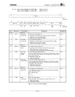
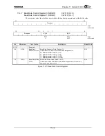
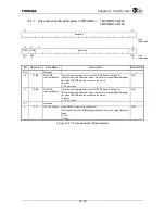
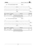
Figure 12.3.3 Operation Example of the Pulse Generator Mode
Count Value
0x000000
TCE = 1
TIMER[n]
Time
TCE = 1
TMCPRBn
Compare Value
TMCPRAn
Compare Value
TMODE1 = 01 (Pulse Generator Mode), CCS= 0 (Internal Clock)
FFI = 1 (Initial High), CRE = 0 (Counter Reset Disable)
TCE = 0
Содержание TX49 TMPR4937
Страница 1: ...64 Bit TX System RISC TX49 Family TMPR4937 Rev 2 0 ...
Страница 4: ......
Страница 13: ...Table of Contents ix TMPR4937 Revision History 1 ...
Страница 14: ...Table of Contents x ...
Страница 15: ...Handling Precautions ...
Страница 16: ......
Страница 18: ...1 Using Toshiba Semiconductors Safely 1 2 ...
Страница 40: ...3 General Safety Precautions and Usage Considerations 3 18 ...
Страница 42: ...4 Precautions and Usage Considerations 4 2 ...
Страница 43: ...TMPR4937 2005 3 Rev 2 0 ...
Страница 44: ......
Страница 52: ...Chapter 1 Overview and Features 1 6 ...
Страница 156: ...Chapter 7 External Bus Controller 7 56 ...
Страница 491: ...Chapter 16 Removed 16 1 16 Removed ...
Страница 492: ...Chapter 16 Removed 16 2 ...
Страница 493: ...Chapter 17 Removed 17 1 17 Removed ...
Страница 494: ...Chapter 17 Removed 17 2 ...
Страница 495: ...Chapter 18 Removed 18 1 18 Removed ...
Страница 496: ...Chapter 18 Removed 18 2 ...
Страница 497: ...Chapter 19 Removed 19 1 19 Removed ...
Страница 498: ...Chapter 19 Removed 19 2 ...
Страница 506: ...Chapter 20 Extended EJTAG Interface 20 8 ...
Страница 529: ...Chapter 22 Pinout and Package Information 22 9 22 2 Package Dimensions P BGA484 3535 1 27B9 Unit mm ...
Страница 530: ...Chapter 22 Pinout and Package Information 22 10 ...
Страница 542: ...Chapter 24 Parts Number when Ordering 24 2 ...
Страница 544: ...Appendix A TX49 H3 Core Supplement A 2 ...


