


Chapter 3 Signals
3-3
3.1.3
External Interface Signals
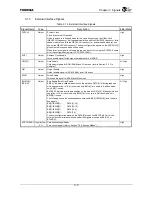
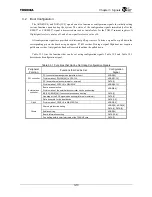
Table 3.1.3 External Interface Signals
Signal Name
Type
Description
Initial State
SYSCLK Output
System
Clock
Clock for external I/O devices.
Outputs a clock in full speed mode (at the same frequency as the G-Bus clock
(GBUSCLK) frequency), half speed mode (at one half the GBUSCLK frequency), third
speed mode (at one third the GBUSCLK frequency), or quarter speed mode (at one
quarter the GBUSCLK frequency). The boot configuration signals on the ADDR[14:13]
pins select which speed mode will be used.
When this clock signal is not used, the pin can be set to H using the SYSCLK Enable
bit of the configuration register (CCFG.SYSCLKEN).
High
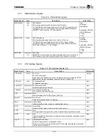
ACE
*
Output
Address Clock Enable
Latch enable signal for the high-order address bits of ADDR.
High
CE[7:0]
*
Output
Chip
Enable
Chip select signals for ROM, SRAM, and I/O devices (refer to Section “3.3 Pin
multiplex”).
All High
OE
*
Output
Output
Enable
Output enable signal for ROM, SRAM, and I/O devices.
High
SWE
*
Output
Write
Enable
Write enable signal for SRAM and I/O devices.
High
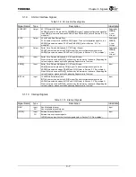
BWE[3:0]
*
/BE[3:0]
*
Output
Byte Enable/Byte Write Enable
BE[3:0]
*
indicate a valid data position on the data bus DATA[31:0] during read and
write bus operation. In 16-bit bus mode, only BE[1:0]
*
are used. In 8-bit bus mode,
only BE[0]
*
is used.
BWE[3:0]
*
indicate a valid data position on the data bus DATA[31:0] during write bus
operation. In 16-bit bus mode, only BWE[1:0]
*
are used. In 8-bit bus mode, only
BWE[0]
*
is used.
The following shows the correspondence between BE[3:0]
*
/BWE[3:0]
*
and the data
bus signals.
BE[3]
*
/BWE[3]
*
: DATA[31:24]
BE[2]
*
/BWE[2]
*
: DATA[23:16]
BE[1]
*
/BWE[1]
*
: DATA[15:8]
BE[0]
*
/BWE[0]
*
: DATA[7:0]
The boot configuration signal on the DATA[5] pin and the EBCCRn.BC bit of the
external bus controller determine whether the signals are used as BE[3:0]
*
or
BWE[3:0]
*
.
All High
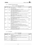
ACK
*
/ READY Input/output
PU
Data Acknowledge/Ready
Flow control signal (refer to Section “7.3.6 Access Modes”).
High
Содержание TX49 TMPR4937
Страница 1: ...64 Bit TX System RISC TX49 Family TMPR4937 Rev 2 0 ...
Страница 4: ......
Страница 13: ...Table of Contents ix TMPR4937 Revision History 1 ...
Страница 14: ...Table of Contents x ...
Страница 15: ...Handling Precautions ...
Страница 16: ......
Страница 18: ...1 Using Toshiba Semiconductors Safely 1 2 ...
Страница 40: ...3 General Safety Precautions and Usage Considerations 3 18 ...
Страница 42: ...4 Precautions and Usage Considerations 4 2 ...
Страница 43: ...TMPR4937 2005 3 Rev 2 0 ...
Страница 44: ......
Страница 52: ...Chapter 1 Overview and Features 1 6 ...
Страница 156: ...Chapter 7 External Bus Controller 7 56 ...
Страница 491: ...Chapter 16 Removed 16 1 16 Removed ...
Страница 492: ...Chapter 16 Removed 16 2 ...
Страница 493: ...Chapter 17 Removed 17 1 17 Removed ...
Страница 494: ...Chapter 17 Removed 17 2 ...
Страница 495: ...Chapter 18 Removed 18 1 18 Removed ...
Страница 496: ...Chapter 18 Removed 18 2 ...
Страница 497: ...Chapter 19 Removed 19 1 19 Removed ...
Страница 498: ...Chapter 19 Removed 19 2 ...
Страница 506: ...Chapter 20 Extended EJTAG Interface 20 8 ...
Страница 529: ...Chapter 22 Pinout and Package Information 22 9 22 2 Package Dimensions P BGA484 3535 1 27B9 Unit mm ...
Страница 530: ...Chapter 22 Pinout and Package Information 22 10 ...
Страница 542: ...Chapter 24 Parts Number when Ordering 24 2 ...
Страница 544: ...Appendix A TX49 H3 Core Supplement A 2 ...


