

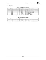


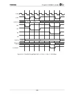
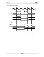
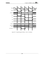

Chapter 9 SDRAM Controller
9-21
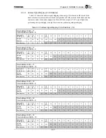
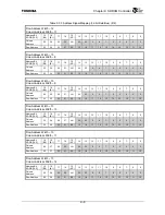
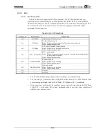
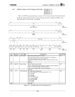
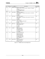
Bit Mnemonic Field
Name
Description
Read/Write
24
ACE
Advanced CKE
Advanced CKE enable (Default: 0)
Enabling this function makes the timing at which CKE changes one cycle
earlier.
0: Disable
1: Enable
R/W
23 PDAE
Power Down
Auto Entry
Power Down Auto Entry Enable (Default: 0)
Enabling this function makes CKE become “L” while the SDRAMC is in the
Idle state. When refresh, memory access, or command execution is
performed, CKE automatically becomes “H”, the requested operation is
performed, then CKE returns to “L” when the operation is complete.
0: Disable
1: Enable
R/W
22:18
RC
Refresh Counter
Refresh Counter (Default: 000000)
This counter is decremented at each refresh. If the refresh circuit is
activated and a value other than “0” is loaded, this field becomes a down
counter that stops at “0”. A value other than “0” must be reloaded to start
the countdown again. This is used during memory initialization.
R/W
17
CASL
CAS Latency
CAS Latency (t
CASL
) (Default: 1)
Specifies the CAS latency.
0: 2 t
CK
1: 3 t
CK
R/W
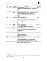
16 DRB
Data Read
Bypass
Data Read Bypass (Default: 0)
Selects the Data Read path used.
0: Data Read latches to the register using the feedback clock.
1: Data Read bypasses the feedback clock latch.
R/W
15 DA
Active Command
Delay
Delay Activate (t
DA
) (Default: 1)
Specifies the delay from the row address to the bank active command.
Setting this bit to “1” sets up the row address two cycles before the active
command is executed.
0: 0 t
CK
1: 1 t
CK
R/W
14
SWB
Slow Write Burst Slow Write Burst (t
SWB
) (Default: 1)
Specifies whether to perform Slow Write Burst.
0: Burst Write occurs at each 1 t
CK
1: Burst Write occurs at each 2 t
CK
R/W
13:12 —
— Reserved
⎯
11:0
RP
Refresh Period
Refresh Period (Default: 0x30c)
Specifies the clock cycle count that generates the refresh cycle. Refresh is
only enabled when at least one SDRAM channel is enabled. Please
program the Timing Register before an arbitrary channel is enabled.
Default is 0x30C. A refresh cycle occurs for each 7.8
µ
s@100 MHz in this
situation.
R/W
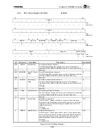
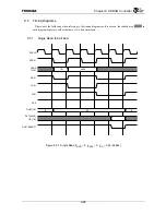
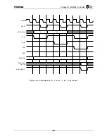
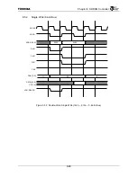
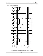
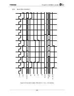
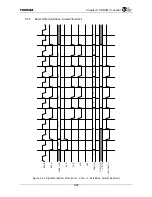
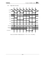
Figure 9.4.2 SDRAM Timing Register (2/2)
1
t
CK
= Clock cycle
2
t
RC
is used during (i) refresh cycle time, (ii) single Read, (iii) two transfer burst Reads. The bank cycle time is t
RAS
+
t
RP
+ 1t
CK
if t
RAS
+ t
RP
< t
RC
in the case of (ii) (iii).
Содержание TX49 TMPR4937
Страница 1: ...64 Bit TX System RISC TX49 Family TMPR4937 Rev 2 0 ...
Страница 4: ......
Страница 13: ...Table of Contents ix TMPR4937 Revision History 1 ...
Страница 14: ...Table of Contents x ...
Страница 15: ...Handling Precautions ...
Страница 16: ......
Страница 18: ...1 Using Toshiba Semiconductors Safely 1 2 ...
Страница 40: ...3 General Safety Precautions and Usage Considerations 3 18 ...
Страница 42: ...4 Precautions and Usage Considerations 4 2 ...
Страница 43: ...TMPR4937 2005 3 Rev 2 0 ...
Страница 44: ......
Страница 52: ...Chapter 1 Overview and Features 1 6 ...
Страница 156: ...Chapter 7 External Bus Controller 7 56 ...
Страница 491: ...Chapter 16 Removed 16 1 16 Removed ...
Страница 492: ...Chapter 16 Removed 16 2 ...
Страница 493: ...Chapter 17 Removed 17 1 17 Removed ...
Страница 494: ...Chapter 17 Removed 17 2 ...
Страница 495: ...Chapter 18 Removed 18 1 18 Removed ...
Страница 496: ...Chapter 18 Removed 18 2 ...
Страница 497: ...Chapter 19 Removed 19 1 19 Removed ...
Страница 498: ...Chapter 19 Removed 19 2 ...
Страница 506: ...Chapter 20 Extended EJTAG Interface 20 8 ...
Страница 529: ...Chapter 22 Pinout and Package Information 22 9 22 2 Package Dimensions P BGA484 3535 1 27B9 Unit mm ...
Страница 530: ...Chapter 22 Pinout and Package Information 22 10 ...
Страница 542: ...Chapter 24 Parts Number when Ordering 24 2 ...
Страница 544: ...Appendix A TX49 H3 Core Supplement A 2 ...


