
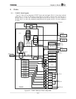


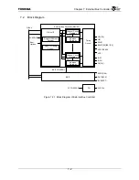


Chapter 7 External Bus Controller
7-7
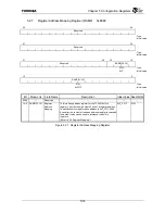
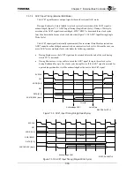
7.3.5
Data Bus Size
The External Bus Controller supports devices with a data bus width of 8 bits, 16 bits, and 32 bits. The
data bus width is selected using the BSZ field of the Channel Control Register (EBCCRn). The address
bits output to each bit of the ADDR[19:0] signal change according to the mode. When access of a size
larger than the data bus width is performed, the dynamic bus sizing function is used to execute multiple
bus access cycles in order from the lower address.
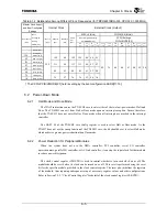
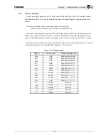
7.3.5.1 32-bit Bus Width Mode
DATA[31:0] becomes valid.
Bits [21:2] of the physical address are output to ADDR[19:0]. The internal address bits [29:22],
which are the upper address, are multiplexed to external ADDR[19:12]. The maximum memory
size is 1 GB.
Table 7.3.4 Address Output Bit Correspondence in the 32-bit Mode
ADDR
Bit 19 18 17 16 15 14 13 12 11 10 9 8
7
6
5 4 3 2 1 0
Upper
Address 29 28
27
26
25
24 23 22
Lower
Address 21 20 19 18 17
16 15 14 13 12 11 10
9 8 7 6 5 4 3 2
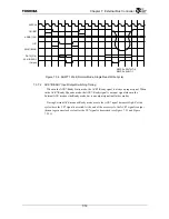
When a Single cycle that accesses 1-Byte/1 half-word/1-word data is executed, 32-bit access is
executed only once on the external bus. 32-bit access is executed twice when performing 1-
double-word access. When a Burst cycle is executed, two 32-bit cycles are executed for each Burst
access when the Bus cycle tries to request a byte combination other than double-word data.
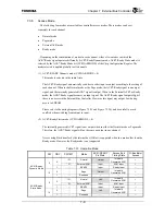
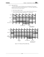
7.3.5.2 16-bit Bus Width Mode
DATA[15:0] becomes valid.
Bits [20:1] of the physical address are output to ADDR[19:0]. The internal address bits [28:21],
which are the upper address, are multiplexed to external ADDR[19:12]. In other words, the
address is shifted up one bit relative to the 32-bit bus mode when output. As a result, the
maximum memory size of the 16-bit bus mode is 512 MB.
Table 7.3.5 Address Output Bit Correspondence in the 16-bit Mode
ADDR
Bit 19 18 17 16 15 14 13 12 11 10 9 8
7
6
5 4 3 2 1 0
Upper Address
28 27 26 25 24 23 22 21
Lower Address
20 19 18 17 16 15 14 13 12 11 10 9 8 7 6 5 4 3 2 1
When a Single cycle that accesses 1-Byte or 1 half-word data is executed, 16-bit access is
executed only once on the external bus. 16-bit access is executed twice when performing 1-word
access. 16-bit access is executed four times when performing 1-double-word access. When a Burst
cycle is executed, four 16-bit cycles are executed for each Burst access when the Bus cycle tries to
request a byte combination other than double-word data.
Содержание TX49 TMPR4937
Страница 1: ...64 Bit TX System RISC TX49 Family TMPR4937 Rev 2 0 ...
Страница 4: ......
Страница 13: ...Table of Contents ix TMPR4937 Revision History 1 ...
Страница 14: ...Table of Contents x ...
Страница 15: ...Handling Precautions ...
Страница 16: ......
Страница 18: ...1 Using Toshiba Semiconductors Safely 1 2 ...
Страница 40: ...3 General Safety Precautions and Usage Considerations 3 18 ...
Страница 42: ...4 Precautions and Usage Considerations 4 2 ...
Страница 43: ...TMPR4937 2005 3 Rev 2 0 ...
Страница 44: ......
Страница 52: ...Chapter 1 Overview and Features 1 6 ...
Страница 156: ...Chapter 7 External Bus Controller 7 56 ...
Страница 491: ...Chapter 16 Removed 16 1 16 Removed ...
Страница 492: ...Chapter 16 Removed 16 2 ...
Страница 493: ...Chapter 17 Removed 17 1 17 Removed ...
Страница 494: ...Chapter 17 Removed 17 2 ...
Страница 495: ...Chapter 18 Removed 18 1 18 Removed ...
Страница 496: ...Chapter 18 Removed 18 2 ...
Страница 497: ...Chapter 19 Removed 19 1 19 Removed ...
Страница 498: ...Chapter 19 Removed 19 2 ...
Страница 506: ...Chapter 20 Extended EJTAG Interface 20 8 ...
Страница 529: ...Chapter 22 Pinout and Package Information 22 9 22 2 Package Dimensions P BGA484 3535 1 27B9 Unit mm ...
Страница 530: ...Chapter 22 Pinout and Package Information 22 10 ...
Страница 542: ...Chapter 24 Parts Number when Ordering 24 2 ...
Страница 544: ...Appendix A TX49 H3 Core Supplement A 2 ...


