


Chapter 8 DMA Controller
8-30
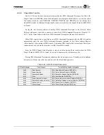
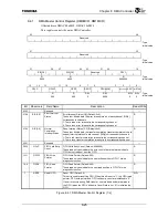
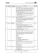
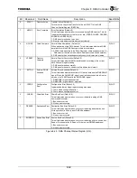
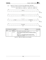
Bit Mnemonic Field
Name
Description Read/Write
9
CHNEN
Chain Enable
Chain Enable (Default: 0)
This bit indicates whether Chain operation is being performed. Read Only.
This bit is cleared when either the Master Enable bit (DMMCR.MSTEN) is
cleared or the Channel Reset bit (DMCCRn.CHRST) is set. This bit is set if
a value other than “0” is set when the CPU writes to the DMA Chain
Address Register (DMCHARn) or when a Chain transfer writes DMA
Command Descriptor. This bit is then cleared when “0” is set to the DMA
Chain Address Register (DMCHARn).
1: If transfer completes due to the current DMA Channel Register setting, a
DMA Command Descriptor is loaded in the DMA Channel Register from
the specified DMA Chain Address Register (DMCHARn) address, then
DMA transfer continues.
0: Further transfer does not start even if transfer completes due to the
current DMA Channel Register setting.
R
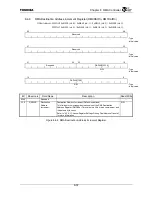
8
XFACT
Transfer Active
Transfer Active (Default: 0)
DMA transfer is performed according to the DMA Channel Register setting
when this bit is set. This bit is automatically set when a value other than “0”
is set in the DMA Chain Address Register (DMCHARn). DMA transfer is
then initiated. This bit is automatically cleared either when DMA transfer
ends normally it is stopped due to an error.
1: Perform DMA transfer.
0: Do not perform DMA transfer.
R/W
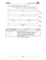
7:6 Reserved
⎯
5 SMPCHN
Simple
Chain Simple
Chain
(Default:
0)
This bit selects the DMA Channel Register that loads data from DMA
Command Descriptors during Chain DMA transfer.
1: Data is only loaded to the four following DMA Channel Registers: the
Chain Address Register (DMCHARn), the Source Address Register
(DMSARn), the Destination Address Register (DMDARn), and the Count
Register (DMCNTRn).
0: Data is loaded to all eight DMA Channel Registers.
R/W
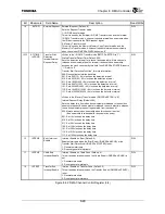
4:2
XFSZ
Transfer Set Size Transfer Set Size (Default: 000)
These bits set the transfer data size of each bus operation in the internal
bus.
When the transfer set size is set to four double words or greater, the data
size actually transferred during a single bus operation does not always
match the transfer set size. Refer to “8.3.7.2 Burst Transfer During Single
Address Transfer” and “8.3.8.2 Burst Transfer During Dual Address
Transfer” for more information.
000: 1 byte
001: 2 byte
010: 4 byte
011: 8 bytes (1double word)
100: 4 double words
101: 8 double words
110: 16 double words (Single Address transfer only)
111: 32 double words (Single Address transfer only)
R/W
1
MEMIO
Memory to I/O
Memory to I/O (Default: 0)
This bit specifies the transfer direction during Single Address transfer
(DMCCRn.SNGAD = 1). Clear this bit when in the Memory Fill Transfer
mode.
The setting of this bit is ignored when Dual Address transfer is set
(DMCCRn.SNGAD = 0).
1: From memory to I/O
0: From I/O to memory
R/W
0
SNGAD
Single Address
Single Address (Default: 0)
This bit specifies whether the transfer method is Single Address transfer or
Dual Address transfer.
1: Single Address transfer
0: Dual Address transfer
R/W
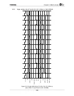
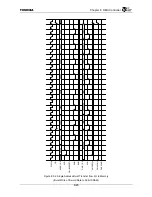
Figure 8.4.2 DMA Channel Control Register (4/4)
Содержание TX49 TMPR4937
Страница 1: ...64 Bit TX System RISC TX49 Family TMPR4937 Rev 2 0 ...
Страница 4: ......
Страница 13: ...Table of Contents ix TMPR4937 Revision History 1 ...
Страница 14: ...Table of Contents x ...
Страница 15: ...Handling Precautions ...
Страница 16: ......
Страница 18: ...1 Using Toshiba Semiconductors Safely 1 2 ...
Страница 40: ...3 General Safety Precautions and Usage Considerations 3 18 ...
Страница 42: ...4 Precautions and Usage Considerations 4 2 ...
Страница 43: ...TMPR4937 2005 3 Rev 2 0 ...
Страница 44: ......
Страница 52: ...Chapter 1 Overview and Features 1 6 ...
Страница 156: ...Chapter 7 External Bus Controller 7 56 ...
Страница 491: ...Chapter 16 Removed 16 1 16 Removed ...
Страница 492: ...Chapter 16 Removed 16 2 ...
Страница 493: ...Chapter 17 Removed 17 1 17 Removed ...
Страница 494: ...Chapter 17 Removed 17 2 ...
Страница 495: ...Chapter 18 Removed 18 1 18 Removed ...
Страница 496: ...Chapter 18 Removed 18 2 ...
Страница 497: ...Chapter 19 Removed 19 1 19 Removed ...
Страница 498: ...Chapter 19 Removed 19 2 ...
Страница 506: ...Chapter 20 Extended EJTAG Interface 20 8 ...
Страница 529: ...Chapter 22 Pinout and Package Information 22 9 22 2 Package Dimensions P BGA484 3535 1 27B9 Unit mm ...
Страница 530: ...Chapter 22 Pinout and Package Information 22 10 ...
Страница 542: ...Chapter 24 Parts Number when Ordering 24 2 ...
Страница 544: ...Appendix A TX49 H3 Core Supplement A 2 ...


