


Chapter 8 DMA Controller
8-25
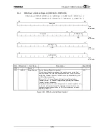
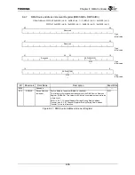
8.4.1
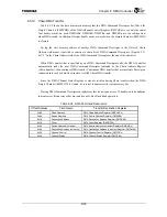
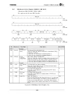
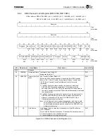
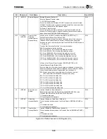
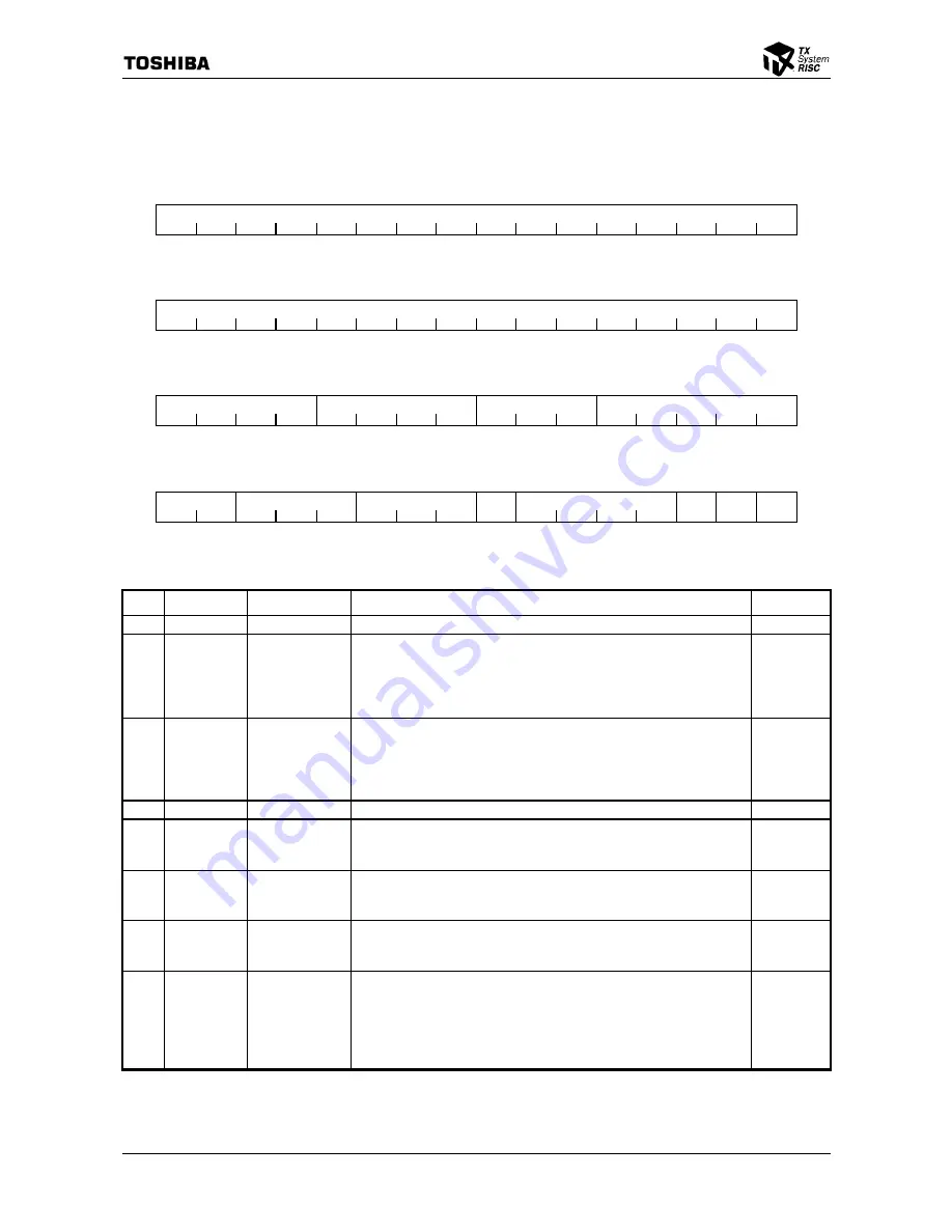
DMA Master Control Register (DM0MCR, DM1MCR)
Offset address: DMAC0 0xB150, DMAC1 0xB950
This register controls the entire DMA Controller.
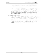
63
48
Reserved
: Type
: Initial value
47
32
Reserved
: Type
: Initial value
31 28 27 24 23 21 20 16
EIS[3:0] DIS[3:0]
Reserved FIFVC
R
R
R
: Type
0000
0000
0000000
: Initial value
15 14
13 11 10 8 7 6 3 2 1 0
FIFVC FIFWP
FIFRP
RSFIF
FIFUM[3:0]
Reserved
RRPT MSTEN
R R
R/W
R/W
R/W
R/W
: Type
000 000 0
0000
0 0
: Initial value
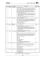
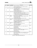
Bit Mnemonic Field
Name
Description Read/Write
63:32 Reserved
⎯
31:28 EIS[3:0] Error Interrupt
Status
Error Interrupt Status [3:0] (Default: 0x0)
These four bits indicate the error interrupt status of each channel. EIS[n]
corresponds to channel
n
.
1: There is an error interrupt in the corresponding channel.
0: There is no error interrupt in the corresponding channel.
R
27:24 DIS[3:0] Normal
Completion
Interrupt Status
Done Interrupt Status [3:0] (Default: 0x0)
These four bits indicate the transfer completion (transfer complete or chain
ended) interrupt status of each channel. DIS[n] corresponds to channel
n
.
1: There is a transfer completion interrupt in the corresponding channel.
0: There is no transfer completion interrupt in the corresponding channel.
R
23:21 Reserved
⎯
20:14 FIFVC FIFO Valid Entry
Count
FIFO Valid Entry Count (Default: 0000000)
These read only bits indicate the byte count of data that were written to
FIFO but not read out from the FIFO.
R
13:11 FIFWP FIFO Write
Pointer
FIFO Write Pointer (Default: 000)
These read only bits indicate the next write position in FIFO. This is a
diagnostic function.
R
10:8 FIFRP FIFO Read
Pointer
FIFO Read Pointer (Default: 000)
These read only bits indicate the next read position in FIFO. This is a
diagnostic function.
R
7
RSFIF
Reset FIFO
Reset FIFO (Default: 0)
This bit is used for resetting FIFO. When this bit is set to “1”, the FIFO read
pointer, FIFO write pointer and FIFO valid entry count are initialized to “0”.
If an error occurs during DMA transfer, use this bit when data remains in
the FIFO (when the FIFO Valid entry Count Field is not “0”) to initialize the
FIFO.
R/W
Figure 8.4.1 DMA Master Control Register (1/2)
Содержание TX49 TMPR4937
Страница 1: ...64 Bit TX System RISC TX49 Family TMPR4937 Rev 2 0 ...
Страница 4: ......
Страница 13: ...Table of Contents ix TMPR4937 Revision History 1 ...
Страница 14: ...Table of Contents x ...
Страница 15: ...Handling Precautions ...
Страница 16: ......
Страница 18: ...1 Using Toshiba Semiconductors Safely 1 2 ...
Страница 40: ...3 General Safety Precautions and Usage Considerations 3 18 ...
Страница 42: ...4 Precautions and Usage Considerations 4 2 ...
Страница 43: ...TMPR4937 2005 3 Rev 2 0 ...
Страница 44: ......
Страница 52: ...Chapter 1 Overview and Features 1 6 ...
Страница 156: ...Chapter 7 External Bus Controller 7 56 ...
Страница 491: ...Chapter 16 Removed 16 1 16 Removed ...
Страница 492: ...Chapter 16 Removed 16 2 ...
Страница 493: ...Chapter 17 Removed 17 1 17 Removed ...
Страница 494: ...Chapter 17 Removed 17 2 ...
Страница 495: ...Chapter 18 Removed 18 1 18 Removed ...
Страница 496: ...Chapter 18 Removed 18 2 ...
Страница 497: ...Chapter 19 Removed 19 1 19 Removed ...
Страница 498: ...Chapter 19 Removed 19 2 ...
Страница 506: ...Chapter 20 Extended EJTAG Interface 20 8 ...
Страница 529: ...Chapter 22 Pinout and Package Information 22 9 22 2 Package Dimensions P BGA484 3535 1 27B9 Unit mm ...
Страница 530: ...Chapter 22 Pinout and Package Information 22 10 ...
Страница 542: ...Chapter 24 Parts Number when Ordering 24 2 ...
Страница 544: ...Appendix A TX49 H3 Core Supplement A 2 ...