


Chapter 7 External Bus Controller
7-24
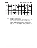
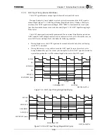
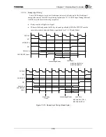
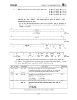
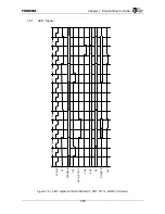
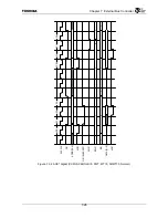
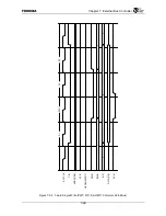
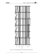
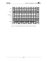
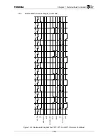
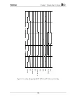
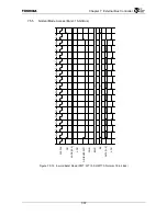
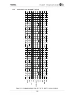
7.5
Timing Diagrams
Please take the following points into account when referring to the timing diagrams.
(1) The clock frequency of the SYSCLK signal can be set to one of the following divisions of the internal
bus clock (GBUSCLK): 1/1, 1/2, 1/3, or 1/4. Also, the operating reference clock frequency can be set to
one of the following divisions of the internal bus clock (GBUSCLK) for each channel: 1/1, 1/2, 1/3, or
1/4. (See 7.3.8.) The timing diagrams indicate the SYSCLK signal clock frequency and channel
operating reference clock frequency as being equivalent.
(2) Both the BWE* signal and BE* signal are indicated in all timing diagrams. The setting of the Channel
Control Register (EBCCRn) determines whether the BWE* pin will function as BWE* or BE*.
(3) All Burst cycles in the timing diagrams illustrate examples in which the address increases by increments
of 1 starting from 0. However, cases where the CWF (Critical Word First) function of the TX49 core
was used or the decrement burst function performed by the DMA Controller was used are exceptions.
(4) The timing diagrams display each clock cycle currently being accessed using the symbols described in
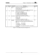
the following table.
SWn
Normal Wait Cycles
PWn
Page Wait Cycles
ASn
Set-up Time from SHWT Address Validation to CE Fall
CSn
Set-up Time from SHWT CE Fall to OE/SWE Fall
AHn
Hold Time from SHWT CE Rise to Address Change
CHn
Hold Time from SHWT OE/SWE Rise to CE Rise
ESn
Synch Cycles of the External Input Signal
ACEn
Address Clock Enable Cycles
Sn Other
Cycles
(5) Shaded areas ( ) in the diagrams are undefined values.
Содержание TX49 TMPR4937
Страница 1: ...64 Bit TX System RISC TX49 Family TMPR4937 Rev 2 0 ...
Страница 4: ......
Страница 13: ...Table of Contents ix TMPR4937 Revision History 1 ...
Страница 14: ...Table of Contents x ...
Страница 15: ...Handling Precautions ...
Страница 16: ......
Страница 18: ...1 Using Toshiba Semiconductors Safely 1 2 ...
Страница 40: ...3 General Safety Precautions and Usage Considerations 3 18 ...
Страница 42: ...4 Precautions and Usage Considerations 4 2 ...
Страница 43: ...TMPR4937 2005 3 Rev 2 0 ...
Страница 44: ......
Страница 52: ...Chapter 1 Overview and Features 1 6 ...
Страница 156: ...Chapter 7 External Bus Controller 7 56 ...
Страница 491: ...Chapter 16 Removed 16 1 16 Removed ...
Страница 492: ...Chapter 16 Removed 16 2 ...
Страница 493: ...Chapter 17 Removed 17 1 17 Removed ...
Страница 494: ...Chapter 17 Removed 17 2 ...
Страница 495: ...Chapter 18 Removed 18 1 18 Removed ...
Страница 496: ...Chapter 18 Removed 18 2 ...
Страница 497: ...Chapter 19 Removed 19 1 19 Removed ...
Страница 498: ...Chapter 19 Removed 19 2 ...
Страница 506: ...Chapter 20 Extended EJTAG Interface 20 8 ...
Страница 529: ...Chapter 22 Pinout and Package Information 22 9 22 2 Package Dimensions P BGA484 3535 1 27B9 Unit mm ...
Страница 530: ...Chapter 22 Pinout and Package Information 22 10 ...
Страница 542: ...Chapter 24 Parts Number when Ordering 24 2 ...
Страница 544: ...Appendix A TX49 H3 Core Supplement A 2 ...


