


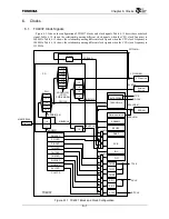


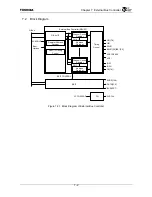


Chapter 7 External Bus Controller
7-4
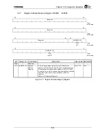
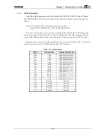
7.3.2 Global/Boot-up
Options
In addition to the settings made separately for each channel, the Channel Control Registers can also
use global options that make settings common to all channels.
External Bus Controller Channel 0 can be used as a Boot memory channel. Channel 0 is set by the
external pins (Boot pins) during reset.
These settings are summarized below in Table 7.3.1. (Please refer to “3.3 Configuration signals” and
“5.2.1 Chip Configuration Register” for more information.)
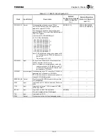
Table 7.3.1 Global/Boot-up Options
Pin Name
Set Register
Explanation
⎯
CCFG.ARMODE
Selects the operation mode of the ACK
*
/READY signal.
0 = ACK
*
/READY Dynamic mode (Default)
1 = ACK
*
/READY Static mode
⎯
CCFG.ACEHOLD
Sets the address hold time relative to the ACE
*
signal.
0: Address changes simultaneous to deassertion of the ACE
*
signal.
1: Address changes 1 clock cycle after deassertion of the ACE
*
signal.
(Default)
ADDR[14:13] CCFG.SYSSP
Specifies the division ratio of the SYSCLK output relative to the internal
bus clock (GBUSCLK).
00: 1/4 speed (1/4 the GBUSCLK frequency)
01: 1/3 speed (1/3 the GBUSCLK frequency)
10: 1/2 speed (1/2 the GBUSCLK frequency)
11: Full speed (same frequency as the GBUSCLK frequency)
ADDR[8] EBCCR0.ME
Specifies whether to enable or disable Channel 0.
0: Disable this channel as a Boot channel.
1: Enable this channel as a Boot channel.
ADDR[7:6] EBCCR0.SP
Specifies the operation speed of Channel 0.
00: 1/4 Speed mode
01: 1/3 Speed mode
10: 1/2 Speed mode
11: Full Speed mode
DATA[5] EBCCR0.BC
When accessing Channel 0, specifies whether to use the BWE[3:0] signal
as a Byte Enable signal (BE[3:0]) or to use it as a Byte Write Enable
signal (BWE[3:0]).
0: Byte Enable mode
1: Byte Write Enable mode
DATA[4] EBCCR0.WT[0]
Specifies the Channel 0 access mode.
0: Normal mode (DATA[4] = H)
1: External ACK mode (DATA[4] = L)
DATA[1:0] EBCCR0.BSZ
Specifies the memory bus width of Channel 0.
00: Reserved
01: 32-bit width
10: 16-bit width
11: 8-bit width
Содержание TX49 TMPR4937
Страница 1: ...64 Bit TX System RISC TX49 Family TMPR4937 Rev 2 0 ...
Страница 4: ......
Страница 13: ...Table of Contents ix TMPR4937 Revision History 1 ...
Страница 14: ...Table of Contents x ...
Страница 15: ...Handling Precautions ...
Страница 16: ......
Страница 18: ...1 Using Toshiba Semiconductors Safely 1 2 ...
Страница 40: ...3 General Safety Precautions and Usage Considerations 3 18 ...
Страница 42: ...4 Precautions and Usage Considerations 4 2 ...
Страница 43: ...TMPR4937 2005 3 Rev 2 0 ...
Страница 44: ......
Страница 52: ...Chapter 1 Overview and Features 1 6 ...
Страница 156: ...Chapter 7 External Bus Controller 7 56 ...
Страница 491: ...Chapter 16 Removed 16 1 16 Removed ...
Страница 492: ...Chapter 16 Removed 16 2 ...
Страница 493: ...Chapter 17 Removed 17 1 17 Removed ...
Страница 494: ...Chapter 17 Removed 17 2 ...
Страница 495: ...Chapter 18 Removed 18 1 18 Removed ...
Страница 496: ...Chapter 18 Removed 18 2 ...
Страница 497: ...Chapter 19 Removed 19 1 19 Removed ...
Страница 498: ...Chapter 19 Removed 19 2 ...
Страница 506: ...Chapter 20 Extended EJTAG Interface 20 8 ...
Страница 529: ...Chapter 22 Pinout and Package Information 22 9 22 2 Package Dimensions P BGA484 3535 1 27B9 Unit mm ...
Страница 530: ...Chapter 22 Pinout and Package Information 22 10 ...
Страница 542: ...Chapter 24 Parts Number when Ordering 24 2 ...
Страница 544: ...Appendix A TX49 H3 Core Supplement A 2 ...