


Chapter 11 Serial I/O Port
11-13
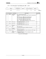
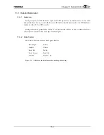
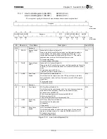
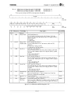
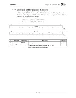
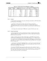
11.4.1 Line Control Register 0 (SILCR0)
0xF300 (Ch. 0)
Line Control Register 1 (SILCR1)
0xF400 (Ch. 1)
These registers specify the format of asynchronous transmission/reception data.
31
16
Reserved
:
Type
:
Initial
value
15
14 13 12 7 6 5 4 3 2 1 0
R/WUB TWUB UODE
Reserved
SCS
UEPS UPEN USBL
UMODE
R/W
R/W
R/W
R/W R/W
R/W
R/W R/W
:
Type
0
1 0
10 0
0
0 00 :
Initial
value
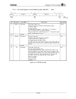
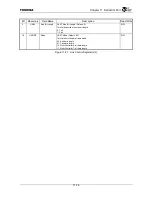
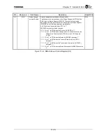
Bit Mnemonic Field
Name
Description
Read/Write
31:16 Reserved
⎯
15 RWUB
Receive
Wake
Up Bit
Wake Up Bit for Receive (Default: 0)
When in the Multi-Controller System mode, this field selects whether to
receive address (ID) frames whose Wake Up bits (WUB) are “1” or to
receive data frames whose Wake Up bits (WUB) are “0”. This value is
undefined when not in the Multi-Controller System mode.
0: Receive data frames.
1: Receive address (ID) frames.
R/W
14 TWUB
Transmit Wake
Up Bit
Wake Up Bit for Transmit (Default: 1)
When in the Multi-Controller System mode, this field specifies the Wake Up
bit (WUB). This value is undefined when not in the Multi-Controller System
mode.
0: Data frame transfer (WUB = 0)
1: Address (ID) frame transfer (WUB = 1)
R/W
13 UODE
Open Drain
Enable
TXD Open Drain Enable (Default: 0)
This field selects the output mode of the TXD signal. When in the Multi-
Controller System mode, the Slave Controller must set the TXD signal to
Open Drain.
0: Totem pole output
1: Open drain output
R/W
12:7 Reserved
⎯
6:5
SCS
Clock Select
SIO Clock Select (Default: 00)
This field selects the serial transfer clock. The clock frequency that is the
serial transfer clock divided by 16 becomes the baud rate (bps).
00: Internal clock (IMBUSCLK)
01: Baud rate generator output that divided IMBUSCLK
10: External clock (SCLK)
11: Baud rate generator output that divided SCLK
R/W
4 UEPS
Even Parity
Select
UART Even Parity Select (Default: 0)
This field selects the parity mode.
0: Odd parity
1: Even parity
R/W
3 UPEN
Parity Check
Enable
UART Parity Enable (Default: 0)
This field selects whether to perform the parity check. This bit must be
cleared in multidrop systems (i.e., when the UMODE field is 10 or 11.)
0: Disable the parity check
1: Enable the parity check
R/W
Figure 11.4.1 Line Control Register (1/2)
Содержание TX49 TMPR4937
Страница 1: ...64 Bit TX System RISC TX49 Family TMPR4937 Rev 2 0 ...
Страница 4: ......
Страница 13: ...Table of Contents ix TMPR4937 Revision History 1 ...
Страница 14: ...Table of Contents x ...
Страница 15: ...Handling Precautions ...
Страница 16: ......
Страница 18: ...1 Using Toshiba Semiconductors Safely 1 2 ...
Страница 40: ...3 General Safety Precautions and Usage Considerations 3 18 ...
Страница 42: ...4 Precautions and Usage Considerations 4 2 ...
Страница 43: ...TMPR4937 2005 3 Rev 2 0 ...
Страница 44: ......
Страница 52: ...Chapter 1 Overview and Features 1 6 ...
Страница 156: ...Chapter 7 External Bus Controller 7 56 ...
Страница 491: ...Chapter 16 Removed 16 1 16 Removed ...
Страница 492: ...Chapter 16 Removed 16 2 ...
Страница 493: ...Chapter 17 Removed 17 1 17 Removed ...
Страница 494: ...Chapter 17 Removed 17 2 ...
Страница 495: ...Chapter 18 Removed 18 1 18 Removed ...
Страница 496: ...Chapter 18 Removed 18 2 ...
Страница 497: ...Chapter 19 Removed 19 1 19 Removed ...
Страница 498: ...Chapter 19 Removed 19 2 ...
Страница 506: ...Chapter 20 Extended EJTAG Interface 20 8 ...
Страница 529: ...Chapter 22 Pinout and Package Information 22 9 22 2 Package Dimensions P BGA484 3535 1 27B9 Unit mm ...
Страница 530: ...Chapter 22 Pinout and Package Information 22 10 ...
Страница 542: ...Chapter 24 Parts Number when Ordering 24 2 ...
Страница 544: ...Appendix A TX49 H3 Core Supplement A 2 ...


