


Chapter 8 DMA Controller
8-28
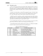
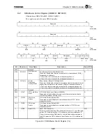
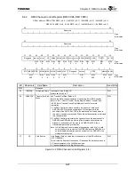
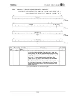
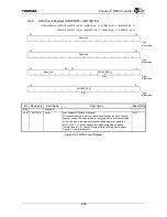
Bit Mnemonic Field
Name
Description Read/Write
26 DBINH
Destination Burst
Inhibit
Destination Burst Inhibit (Default: 0)
During Dual Address transfer, this bit sets whether to perform Burst
transfer or Single transfer on a Write cycle to the address set from FIFO to
DMDARn when Burst transfer is set by DMCCRn.XFSZ. Refer to “8.3.8.2
Burst Transfer During Dual Address Transfer” for more information.
The settings of this bit have no effect during Single Address transfers.
1: Multiple Single transfers are executed.
0: Burst transfer is executed.
R/W
25 SBINH
Source Burst
Inhibit
Source Burst Inhibit (Default: 0)
During Dual Address transfer, this bit sets whether to perform Burst
transfer or Single transfer on a Read cycle to the FIFO from the address
set to DMSARn when Burst transfer is set by DMCCRn.XFSZ. Refer to
“8.3.8.2 Burst Transfer During Dual Address Transfer” for more
information.
The settings of this bit have no effect during Single Address transfers.
1: Multiple Single transfers are executed.
0: Burst transfer is executed.
R/W
24 CHRST
Channel
Reset Channel Reset (Default: 1)
This bit is used fo initializing channels. The DMCCRn.XFACT,
DMCCRn.CHNEN, and DMCSRn bits are all cleared. In addition, all
channel logic and interrupts from channels are cleared and bus ownership
requests to the DMA Channel Arbiter are also reset. The software must
clear this bit before operating a channel.
1: Reset channel
0: Enable channel
R/W
23 REVBYTE
Reverse
Byte Reverse Bytes (Default: 0)
This bit specifies whether to reverse the byte order during a Dual Address
transfer when the Transfer Setting Size field (DMCCRn.XFSZ) setting is 8
bytes or more. Refer to “8.3.8.3 Double Word Byte Swapping” for more
information.
1: Reverses the byte order.
0: Does not reverse the byte order.
R/W
22 ACKPOL
Acknowledge
Polarity
Acknowledge Polarity (Default: 0)
Specifies the polarity of the DMAACK[n] signal.
1: Asserts when the DMAACK[n] signal is High
0: Asserts when the DMAACK[n] signal is Low
R/W
21 REQPL
Request
Polarity
Request Polarity (Default: 0)
Specifies the polarity of the DMAREQ[n] signal.
1: Asserts when the DMAREQ[n] signal is High.
0: Asserts when the DMAREQ[n] signal is Low.
R/W
20 EGREQ
Edge
Request Edge Request (Default: 0)
Specifies the method for detecting DMA requests by the DMAREQ[n]
signal.
1: DMAREQ[n] signal is Edge Detect.
0: DMAREQ[n] signal is Level Detect.
R/W
19 CHDN
Chain
Complete
Chain Done (Default: 0)
Selects control by the DMADONE
*
signal. See “8.3.3.4 DMA Controller”
for more information.
1: Assertion of the DMADONE
*
signal controls the overall Chain DMA
transfer.
0: Assertion of the DMADONE
*
signal controls DMA transfer according to
the DMA Channel Register setting at that time.
R/W
18:17
DNCTL
DONE Control
Done Control (Default: 00)
Specifies the input/output mode of the DMADONE
*
signal. Refer to
“8.3.3.4 DMADONE* Signal” for more information.
00: DMADONE
*
signal becomes the input signal, but input is ignored.
01: DMADONE
*
signal becomes the input signal.
10: DMADONE
*
signal becomes the output signal.
11: DMADONE
*
signal becomes the open drain input/output signal.
R/W
Figure 8.4.2 DMA Channel Control Register (2/4)
Содержание TX49 TMPR4937
Страница 1: ...64 Bit TX System RISC TX49 Family TMPR4937 Rev 2 0 ...
Страница 4: ......
Страница 13: ...Table of Contents ix TMPR4937 Revision History 1 ...
Страница 14: ...Table of Contents x ...
Страница 15: ...Handling Precautions ...
Страница 16: ......
Страница 18: ...1 Using Toshiba Semiconductors Safely 1 2 ...
Страница 40: ...3 General Safety Precautions and Usage Considerations 3 18 ...
Страница 42: ...4 Precautions and Usage Considerations 4 2 ...
Страница 43: ...TMPR4937 2005 3 Rev 2 0 ...
Страница 44: ......
Страница 52: ...Chapter 1 Overview and Features 1 6 ...
Страница 156: ...Chapter 7 External Bus Controller 7 56 ...
Страница 491: ...Chapter 16 Removed 16 1 16 Removed ...
Страница 492: ...Chapter 16 Removed 16 2 ...
Страница 493: ...Chapter 17 Removed 17 1 17 Removed ...
Страница 494: ...Chapter 17 Removed 17 2 ...
Страница 495: ...Chapter 18 Removed 18 1 18 Removed ...
Страница 496: ...Chapter 18 Removed 18 2 ...
Страница 497: ...Chapter 19 Removed 19 1 19 Removed ...
Страница 498: ...Chapter 19 Removed 19 2 ...
Страница 506: ...Chapter 20 Extended EJTAG Interface 20 8 ...
Страница 529: ...Chapter 22 Pinout and Package Information 22 9 22 2 Package Dimensions P BGA484 3535 1 27B9 Unit mm ...
Страница 530: ...Chapter 22 Pinout and Package Information 22 10 ...
Страница 542: ...Chapter 24 Parts Number when Ordering 24 2 ...
Страница 544: ...Appendix A TX49 H3 Core Supplement A 2 ...


