


Chapter 10 PCI Controller
10-38
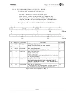
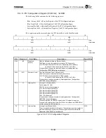
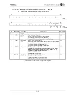
10.4.13 PCI Configuration 2 Register (PCICFG2) 0xD03C
The following fields correspond to the following registers:
Max. Latency field
→
Max_Lat Register of the PCI Configuration Space
Min. Grant field
→
Min_Gnt Register of the PCI Configuration Space
Interrupt Pin field
→
Interrupt Pin Register of the PCI Configuration Space
Interrupt
Line
field
→
Interrupt Line Register of the PCI Configuration Space
This register cannot be accessed when the PCI Controller is in the Satellite mode.
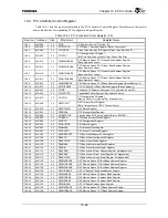
31
24
23 16
ML MG
R/L R/L
:
Type
0x0A
0x02
: Initial value
15
8 7 0
IP IL
R/L R/W
:
Type
0x01
0x00
: Initial value
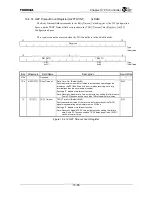
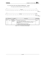
Bits Mnemonic Field
Name
Description
Read/Write
31:24 ML Maximum
Latency
Max_Lat (Maximum Latency) (Default: 0x0A)
00h: Does not use this register to determine PCI Bus priority.
01h-FFh: Specifies the time interval for requesting bus ownership.
In units of 250 ns, assuming the PCICLK is 33 MHz.
It is possible to change the maximum latency by loading data from
Configuration EEPROM during initialization.
R/L
23:16
MG
Minimum Grant
Min_Gnt (Minimum Grant) (Default: 0x02)
00h: Is not used to calculate the latency timer value.
01h-FFh: Sets the time required for Burst transfer.
In units of 250 ns, assuming the PCICLK is 33 MHz.
It is possible to change this value by loading data from Configuration
EEPROM during initialization.
R/L
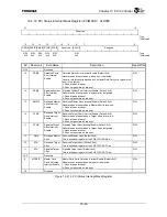
15:8
IP
Interrupt Pin
Interrupt Pin (Default: 0x01)
Valid values: 00 - 04h
00h: Do not use interrupt signals.
01h: Use Interrupt signal INTA
*
02h: Use Interrupt signal INTB
*
03h: Use Interrupt signal INTC
*
04h: Use Interrupt signal INTD
*
05h - FFh: Reserved
It is possible to change this value by loading data from Configuration
EEPROM during initialization.
When using either the REQ[2]
*
signal or the PIO signal to report an
interrupt to an external device as the PCI device, please use EEPROM to
set the connection with that device.
R/L
7:0
IL
Interrupt Line
Interrupt Line (Default: 0x00)
This is a readable/writable 8-bit register. The software uses this register to
indicate information such as the interrupt signal connection information.
Operation of the TX4937 is not affected.
R/W
Figure 10.4.11 PCI Configuration 2 Register
Содержание TX49 TMPR4937
Страница 1: ...64 Bit TX System RISC TX49 Family TMPR4937 Rev 2 0 ...
Страница 4: ......
Страница 13: ...Table of Contents ix TMPR4937 Revision History 1 ...
Страница 14: ...Table of Contents x ...
Страница 15: ...Handling Precautions ...
Страница 16: ......
Страница 18: ...1 Using Toshiba Semiconductors Safely 1 2 ...
Страница 40: ...3 General Safety Precautions and Usage Considerations 3 18 ...
Страница 42: ...4 Precautions and Usage Considerations 4 2 ...
Страница 43: ...TMPR4937 2005 3 Rev 2 0 ...
Страница 44: ......
Страница 52: ...Chapter 1 Overview and Features 1 6 ...
Страница 156: ...Chapter 7 External Bus Controller 7 56 ...
Страница 491: ...Chapter 16 Removed 16 1 16 Removed ...
Страница 492: ...Chapter 16 Removed 16 2 ...
Страница 493: ...Chapter 17 Removed 17 1 17 Removed ...
Страница 494: ...Chapter 17 Removed 17 2 ...
Страница 495: ...Chapter 18 Removed 18 1 18 Removed ...
Страница 496: ...Chapter 18 Removed 18 2 ...
Страница 497: ...Chapter 19 Removed 19 1 19 Removed ...
Страница 498: ...Chapter 19 Removed 19 2 ...
Страница 506: ...Chapter 20 Extended EJTAG Interface 20 8 ...
Страница 529: ...Chapter 22 Pinout and Package Information 22 9 22 2 Package Dimensions P BGA484 3535 1 27B9 Unit mm ...
Страница 530: ...Chapter 22 Pinout and Package Information 22 10 ...
Страница 542: ...Chapter 24 Parts Number when Ordering 24 2 ...
Страница 544: ...Appendix A TX49 H3 Core Supplement A 2 ...


